EP0567955A2 - Bildelementkompensationsschaltung für Bildsensor - Google Patents
Bildelementkompensationsschaltung für Bildsensor Download PDFInfo
- Publication number
- EP0567955A2 EP0567955A2 EP93106660A EP93106660A EP0567955A2 EP 0567955 A2 EP0567955 A2 EP 0567955A2 EP 93106660 A EP93106660 A EP 93106660A EP 93106660 A EP93106660 A EP 93106660A EP 0567955 A2 EP0567955 A2 EP 0567955A2
- Authority
- EP
- European Patent Office
- Prior art keywords
- color
- signals
- dot
- signal
- pixels
- Prior art date
- Legal status (The legal status is an assumption and is not a legal conclusion. Google has not performed a legal analysis and makes no representation as to the accuracy of the status listed.)
- Granted
Links
Images

Classifications
-
- H—ELECTRICITY
- H04—ELECTRIC COMMUNICATION TECHNIQUE
- H04N—PICTORIAL COMMUNICATION, e.g. TELEVISION
- H04N23/00—Cameras or camera modules comprising electronic image sensors; Control thereof
- H04N23/80—Camera processing pipelines; Components thereof
- H04N23/84—Camera processing pipelines; Components thereof for processing colour signals
- H04N23/88—Camera processing pipelines; Components thereof for processing colour signals for colour balance, e.g. white-balance circuits or colour temperature control
-
- H—ELECTRICITY
- H04—ELECTRIC COMMUNICATION TECHNIQUE
- H04N—PICTORIAL COMMUNICATION, e.g. TELEVISION
- H04N25/00—Circuitry of solid-state image sensors [SSIS]; Control thereof
- H04N25/10—Circuitry of solid-state image sensors [SSIS]; Control thereof for transforming different wavelengths into image signals
- H04N25/11—Arrangement of colour filter arrays [CFA]; Filter mosaics
- H04N25/13—Arrangement of colour filter arrays [CFA]; Filter mosaics characterised by the spectral characteristics of the filter elements
- H04N25/135—Arrangement of colour filter arrays [CFA]; Filter mosaics characterised by the spectral characteristics of the filter elements based on four or more different wavelength filter elements
- H04N25/136—Arrangement of colour filter arrays [CFA]; Filter mosaics characterised by the spectral characteristics of the filter elements based on four or more different wavelength filter elements using complementary colours
-
- H—ELECTRICITY
- H04—ELECTRIC COMMUNICATION TECHNIQUE
- H04N—PICTORIAL COMMUNICATION, e.g. TELEVISION
- H04N25/00—Circuitry of solid-state image sensors [SSIS]; Control thereof
- H04N25/70—SSIS architectures; Circuits associated therewith
- H04N25/71—Charge-coupled device [CCD] sensors; Charge-transfer registers specially adapted for CCD sensors
- H04N25/73—Charge-coupled device [CCD] sensors; Charge-transfer registers specially adapted for CCD sensors using interline transfer [IT]
Definitions
- the present invention generally relates to carrier level balancing circuits in a color camera signal processing circuit and, more particularly, to a carrier level balancing circuit for use in a signal processing circuit of a color camera formed of a CCD (charge-coupled device) solid state image pickup device of a so-called all pixel separately read out type in which signal charges of all pixels are separately read out during one field period.
- CCD charge-coupled device
- a color camera formed of a CCD solid state image pickup device of a so-called two-pixel mixing type in which signal charges of two pixels adjacent in the vertical direction are mixed and read out is disclosed in FIG. 12 of Japanese laid-open patent publication No. 63-301687, for example.
- this kind of CCD solid state image pickup device output signals read out by mixing two pixels at every field are respectively multiplied with proper different coefficients thereby to balance carrier levels of the respective output signals. Then, the occurrence of a color aliasing signal in a luminance signal is suppressed by generating a luminance signal from the output signal whose carrier level was balanced.
- a CCD solid state image pickup device of an all pixel separately read out type is known to improve a vertical resolution as is disclosed in Japanese laid-open patent publication No. 63-301687.
- a carrier level balancing circuit for a color camera formed of a solid state image pickup device in which signal charges of all pixels are separately read out at every two lines during one field period and then output as dot-sequential two-channel color signals.
- This carrier level balancing circuit comprises a first multiplier for alternately multiplying one of the two-channel color signals with first and second coefficients set in association with respective color signals in response to a color temperature information at the unit of pixel, a second multiplier for alternately multiplying the other of the two-channel color signals with third and fourth coefficients set in association with respective color signals in response to a color temperature information at the unit of pixel and an adding circuit for adding the two-channel color signals processed by the first and second multipliers by two pixels each.
- a carrier level balancing circuit which comprises a color signal converting circuit for converting two-channel color signals into a first color signal formed of a combination of pixels of the same color and a second color signal formed of a combination of pixels of different colors, a first multiplier for multiplying the first color signal with a first coefficient set in response to a color temperature information, a second multiplier for alternately multiplying the second color signal with second and third coefficients set in response to a color temperature information at the unit of pixel and an adding circuit for adding the first and second color signals from the first and second multipliers by two pixels each.
- the coefficients that are separately set at every line in response to the color temperature information are multiplied to the two-channel color signals output from the solid state image pickup device while the respective coefficients are being switched in a dot-sequential fashion thereby to balance carrier levels.
- the two-channel color signals output from the solid state image pickup device are converted into the color signal formed by a combination of pixels of the same color and the color signal formed by a combination of pixels of different colors. Then, the same coefficient is constantly multiplied to these color signals with respect to the line formed by a combination of the pixels of the same color and the independent coefficients are multiplied to these color signals with respect to the line formed by a combination of the pixels of different colors in a dot-sequential fashion thereby to balance carrier levels.
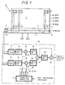
- FIG. 1 of the accompanying drawings is a block diagram illustrative of a carrier level balancing circuit for a color camera formed of a CCD solid state image pickup device of an all pixel separately read out type which is applied to the processing of a luminance signal.
- an image pickup area 3 comprises a plurality of photo-sensors 1 that are arranged at the unit of pixels in a two-dimensional fashion to accumulate a signal charge corresponding to an incident light thereon and vertical CCDs 2 for transferring signal charges read out from the photo-sensors 1 at every vertical column in the vertical direction.
- a color filter array (not shown) is formed on the image pickup area 3,
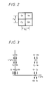
- the color filter arrangement may be of the line sequential type formed of a G (green) checkered Ye (yellow)/ Cy (cyan) as shown in FIG. 2 and four pixels are employed as a basic unit.
- reference symbol Px designates a pixel pitch in the horizontal direction
- Py designates a pixel pitch in the vertical direction, respectively.
- the vertical CCD 2 effects the operation corresponding to the vertical scanning and is driven by four-phase vertical transfer clocks ⁇ V1 to ⁇ V4.
- Two horizontal CCDs 4, 5 for transferring signal charges, transferred from the vertical CCD 2, in the horizontal direction are disposed in parallel to the output side of the vertical CCD 2.
- the horizontal CCDs 4, 5 effect the operation corresponding to the horizontal scanning and are driven by two-phase horizontal transfer clocks ⁇ H1 and ⁇ H2. Signal charges of two lines each are transferred to the horizontal CCDs 4, 5 from the vertical CCD 2 and the distribution of signal charges to the two horizontal CCDs 4, 5 is effected at the unit of line by a distribution transfer gate 6 disposed between the horizontal CCDs 4, 5.
- output sections 7, 8 that are formed of floating diffusion amplifiers to detect and convert transferred signal charges into signal voltages. These output sections 7, 8 derive two-channel pixel signals simultaneously.
- the CCD solid state image pickup device 9 of all pixel separately read out type is constructed to separately read out signal charges of all pixels at every two lines during one field period and to output the same as dot-sequential two-channel pixel signals (color signals).
- the two-channel output signals from the CCD solid state image pickup device 9 are supplied through a CDS (correlated double sampling) circuit (not shown) and a sample and hold circuit (not shown) to a carrier level balancing circuit 10 according to the present invention.
- CDS correlated double sampling
- sample and hold circuit not shown
- the two-channel signals are converted into digital signals by A/D (analog-to-digital) converters 11, 12, latched by latch circuits 13, 14 which latch data of one pixel and then input to multipliers 15, 16.
- A/D analog-to-digital
- the multipliers 15, 16 are supplied with carrier balance coefficients a/b and c/d which are set by a coefficient setting circuit 17 and which are alternately output from the coefficient setting circuit 17 under the control of a change-over switch 18.
- the carrier balance coefficients a/b and c/d are respectively multiplied to the two-channel pixel signals by the multipliers 15 and 16.
- the change-over switch 18 is changed in position in response to a switching frequency of 2fsc when a sampling frequency of the two-channel pixel signals is set to 4fsc where fsc is the color sub-carrier frequency of the color signal.
- the coefficient setting circuit 17 sets carrier balance coefficients a, b, c, and d corresponding to color signals Gr, Ye, Cy and Gb in response to a color temperature information calculated on the basis of the output signal from the CCD solid state image pickup device 9, for example.
- the two-channel pixel signals (a*Gr/b*Ye, c*Cy/d*Gb) that were multiplied with the carrier balance coefficients a/b and c/d are latched by one-bit latch circuits 19, 20 and then added with each other by an adder 21.
- adder 21 By this adding processing in the adder 21, pixel signals of two pixels adjacent in the vertical direction are added.
- An added output from the adder 21 is added with an added output of one pixel before latched in a latch circuit 23 by an adder 22.
- the pixel signals of adjacent four pixels in the vertical and horizontal directions are added with one another while the color filter array shown in FIG. 2 is taken as a basic unit, and thereby being output as a luminance signal Y.
- the independent carrier balance coefficients a, b, c, d are multiplied to the respective color signals from the CCD solid state image pickup device 9 at every lines (Gr/Ye/ and Cy/Gb lines) while these coefficients a, b, c, d are being switched in a dot-sequential fashion in response to the switching clock having the frequency of 2fsc and the values of these coefficients a, b, c, d are set in response to the color temperature information, whereby carrier levels can be balanced at all sorts of color temperatures.
- the carrier levels of the respective pixel signals are balanced so that the levels of all carriers of the color signals Gr, Ye, Cy and Gb become the same as shown in FIG. 3.
- the color aliasing signals can be canceled completely in the vertical, horizontal and oblique directions.
- FIG. 4 is a block diagram showing another embodiment of the present invention.
- like parts corresponding to those of FIG. 1 are marked with the same references and therefore need not be described in detail.
- the two-channel pixel signals Gr/Ye and Cy/Gb output from the CCD solid state image Pickup device 9 are switched by change-over circuits 24, 25 in response to the switching clock having the frequency 2fsc and thereby converted into respective color signals of Gr/Gb lines and Cy/Ye lines.
- These color signals are constantly multiplied with the same carrier balance coefficient a by the multiplier 15 with respect to the Gr/Gb lines because the signals Gr and Gb are considered to be the G signals of the same level.
- these color signals are respectively multiplied with independent carrier balance coefficients b and c by the multiplier 16 with respect to the Cy/Ye lines in a dot-sequential fashion.
- These carrier balance coefficients a, b and c are set by a coefficient setting circuit (not shown) in response to the color temperature information.
- the multiplied results are added by the adder 21 and the added output from the adder 21 is added with an added output of one pixel before latched by the latch circuit 23 by the adder 22 which thus derives the luminance signal Y.
- the carrier levels of respective color signals can be balanced at all sorts of color temperatures similarly to the first embodiment. Therefore, the color aliasing signals can be completely canceled in the vertical, horizontal and oblique directions.
- the carrier level balancing circuit of the present invention is applied to the luminance signal processing as described above, the present invention is not limited thereto and the same circuit arrangement of this carrier level balancing circuit can be applied to an aperture control signal that controls an aperture correcting circuit for correcting a high frequency component signal from a circuit standpoint or the like. Therefore, the processing of the aperture control signal in which the color aliasing signal can be prevented from occurring becomes possible.
- the coefficients that are independently set in response to the color temperature information are multiplied to the two-channel color signals output from the solid state image pickup device while the respective coefficients are being switched in a dot-sequential fashion thereby to balance carrier levels.
- the two-channel color signals output from the solid state image pickup device are converted into the color signal formed by a combination of pixels of the same color and the color signal formed by a combination of pixels of different colors.
- the same coefficient is constantly multiplied to these color signals with respect to the line formed of a combination of the pixels of the same color and the independent coefficients are multiplied to these color signals with respect to the line formed of a combination of the pixels of different colors in a dot-sequential fashion thereby to balance carrier levels. Therefore, in addition to the above-mentioned effect, there can be achieved the effect such that only three carrier balance coefficients are set.
Landscapes
- Engineering & Computer Science (AREA)
- Multimedia (AREA)
- Signal Processing (AREA)
- Physics & Mathematics (AREA)
- Spectroscopy & Molecular Physics (AREA)
- Color Television Image Signal Generators (AREA)
- Television Receiver Circuits (AREA)
- Processing Of Color Television Signals (AREA)
Applications Claiming Priority (2)
| Application Number | Priority Date | Filing Date | Title |
|---|---|---|---|
| JP136058/92 | 1992-04-27 | ||
| JP4136058A JPH05304679A (ja) | 1992-04-27 | 1992-04-27 | カラーカメラの信号処理回路におけるレベルバランス回路 |
Publications (3)
| Publication Number | Publication Date |
|---|---|
| EP0567955A2 true EP0567955A2 (de) | 1993-11-03 |
| EP0567955A3 EP0567955A3 (en) | 1994-06-22 |
| EP0567955B1 EP0567955B1 (de) | 1997-06-18 |
Family
ID=15166214
Family Applications (1)
| Application Number | Title | Priority Date | Filing Date |
|---|---|---|---|
| EP93106660A Expired - Lifetime EP0567955B1 (de) | 1992-04-27 | 1993-04-23 | Bildelementkompensationsschaltung für Bildsensor |
Country Status (5)
| Country | Link |
|---|---|
| US (1) | US5387931A (de) |
| EP (1) | EP0567955B1 (de) |
| JP (1) | JPH05304679A (de) |
| KR (1) | KR100261130B1 (de) |
| DE (1) | DE69311624T2 (de) |
Cited By (3)
| Publication number | Priority date | Publication date | Assignee | Title |
|---|---|---|---|---|
| EP0710034A3 (de) * | 1994-10-31 | 1996-10-23 | Symbios Logic Inc | Vorrichtung und Verfahren zur Bildabtastung mit einer Sensoranordnung |
| US5754342A (en) * | 1993-03-31 | 1998-05-19 | Kuraray Co., Ltd. | Video device utilizing a two-dimensional diffraction grating |
| EP0835030A3 (de) * | 1996-10-02 | 2000-03-15 | Gec-Marconi Limited | Farbfernsehkamera |
Families Citing this family (1)
| Publication number | Priority date | Publication date | Assignee | Title |
|---|---|---|---|---|
| US8305387B2 (en) * | 2007-09-07 | 2012-11-06 | Texas Instruments Incorporated | Adaptive pulse-width modulated sequences for sequential color display systems |
Family Cites Families (6)
| Publication number | Priority date | Publication date | Assignee | Title |
|---|---|---|---|---|
| EP0138074B1 (de) * | 1983-09-16 | 1989-12-13 | Hitachi, Ltd. | Signalverarbeitungsschaltung für eine Farbvideokamera |
| US4714955A (en) * | 1985-11-06 | 1987-12-22 | Hitachi, Ltd. | Solid-state color image pickup apparatus |
| JPH074017B2 (ja) * | 1985-11-09 | 1995-01-18 | キヤノン株式会社 | 撮像装置 |
| JPS6369393A (ja) * | 1986-09-11 | 1988-03-29 | Sanyo Electric Co Ltd | モアレ防止回路 |
| JP2748442B2 (ja) * | 1988-10-13 | 1998-05-06 | ソニー株式会社 | カラー映像信号の処理装置 |
| US5198890A (en) * | 1989-03-30 | 1993-03-30 | Canon Kabushiki Kaisha | White balance correcting device for an image sensing |
-
1992
- 1992-04-27 JP JP4136058A patent/JPH05304679A/ja active Pending
-
1993
- 1993-04-22 KR KR1019990006756A patent/KR100261130B1/ko not_active Expired - Lifetime
- 1993-04-22 US US08/050,652 patent/US5387931A/en not_active Expired - Lifetime
- 1993-04-23 DE DE69311624T patent/DE69311624T2/de not_active Expired - Fee Related
- 1993-04-23 EP EP93106660A patent/EP0567955B1/de not_active Expired - Lifetime
Cited By (3)
| Publication number | Priority date | Publication date | Assignee | Title |
|---|---|---|---|---|
| US5754342A (en) * | 1993-03-31 | 1998-05-19 | Kuraray Co., Ltd. | Video device utilizing a two-dimensional diffraction grating |
| EP0710034A3 (de) * | 1994-10-31 | 1996-10-23 | Symbios Logic Inc | Vorrichtung und Verfahren zur Bildabtastung mit einer Sensoranordnung |
| EP0835030A3 (de) * | 1996-10-02 | 2000-03-15 | Gec-Marconi Limited | Farbfernsehkamera |
Also Published As
| Publication number | Publication date |
|---|---|
| KR930022894A (ko) | 1993-11-24 |
| DE69311624T2 (de) | 1998-01-15 |
| EP0567955B1 (de) | 1997-06-18 |
| DE69311624D1 (de) | 1997-07-24 |
| KR100261130B1 (ko) | 2000-07-01 |
| EP0567955A3 (en) | 1994-06-22 |
| US5387931A (en) | 1995-02-07 |
| JPH05304679A (ja) | 1993-11-16 |
Similar Documents
| Publication | Publication Date | Title |
|---|---|---|
| US5374956A (en) | Electronic imaging apparatus with dithered color filter array | |
| US5018006A (en) | Multi-plate type image pickup apparatus having picture elements for producing color and luminance signals | |
| KR100468169B1 (ko) | 위색(僞色)신호발생이억제가능한단판식컬러카메라 | |
| EP0368354B1 (de) | Signalverarbeitungsschaltung für eine Festkörperbildaufnahmevorrichtung | |
| EP0494677B1 (de) | Farbmatrixschaltung für eine CCD-Farbkamera | |
| KR20070090106A (ko) | 카메라 시스템의 제어방법 및 그 방법을 이용한 카메라시스템 | |
| EP0520759B1 (de) | Festkörperkamera | |
| US4821088A (en) | Solid-state color image pickup unit with mosaic color filter and two horizontal output registers | |
| KR19990063462A (ko) | 화상 신호 처리 장치 | |
| US4907074A (en) | Image pickup apparatus having color separation filters and forming line-sequential luminance and color-difference signals | |
| KR100447916B1 (ko) | 고해상도이며의사색의발생을억제할수있는단판식컬러카메라 | |
| EP0558338A2 (de) | Videokamera | |
| US6822680B1 (en) | One-chip color camera that can suppress generation of pseudo color signal while maintaining high resolution and method of separating color data | |
| US5387931A (en) | Carrier level balancing circuit for color camera | |
| JPH0459832B2 (de) | ||
| US4646139A (en) | Color image pickup apparatus with color filter array comprising filter elements of three different colors arranged to provide reduced folding distortion | |
| JPH0823541A (ja) | カラー撮像装置 | |
| JP2624657B2 (ja) | 固体カラーカメラ | |
| JP3422027B2 (ja) | カラーカメラ及びその信号処理回路における輝度バランス回路 | |
| JPH05916B2 (de) | ||
| EP0485221A2 (de) | Festkörper-Bildaufnahmevorrichtung mit einem Farbfilter | |
| WO2002085035A1 (fr) | Dispositif d'imagerie a semiconducteur | |
| JPH0468837B2 (de) | ||
| JP2585461B2 (ja) | 固体カラーカメラ | |
| JPH0132712B2 (de) |
Legal Events
| Date | Code | Title | Description |
|---|---|---|---|
| PUAI | Public reference made under article 153(3) epc to a published international application that has entered the european phase |
Free format text: ORIGINAL CODE: 0009012 |
|
| AK | Designated contracting states |
Kind code of ref document: A2 Designated state(s): DE FR GB |
|
| PUAL | Search report despatched |
Free format text: ORIGINAL CODE: 0009013 |
|
| AK | Designated contracting states |
Kind code of ref document: A3 Designated state(s): DE FR GB |
|
| 17P | Request for examination filed |
Effective date: 19941123 |
|
| 17Q | First examination report despatched |
Effective date: 19950721 |
|
| GRAG | Despatch of communication of intention to grant |
Free format text: ORIGINAL CODE: EPIDOS AGRA |
|
| GRAH | Despatch of communication of intention to grant a patent |
Free format text: ORIGINAL CODE: EPIDOS IGRA |
|
| GRAH | Despatch of communication of intention to grant a patent |
Free format text: ORIGINAL CODE: EPIDOS IGRA |
|
| GRAA | (expected) grant |
Free format text: ORIGINAL CODE: 0009210 |
|
| AK | Designated contracting states |
Kind code of ref document: B1 Designated state(s): DE FR GB |
|
| REF | Corresponds to: |
Ref document number: 69311624 Country of ref document: DE Date of ref document: 19970724 |
|
| ET | Fr: translation filed | ||
| PLBE | No opposition filed within time limit |
Free format text: ORIGINAL CODE: 0009261 |
|
| 26N | No opposition filed | ||
| REG | Reference to a national code |
Ref country code: GB Ref legal event code: IF02 |
|
| PGFP | Annual fee paid to national office [announced via postgrant information from national office to epo] |
Ref country code: FR Payment date: 20090417 Year of fee payment: 17 Ref country code: DE Payment date: 20090420 Year of fee payment: 17 |
|
| PGFP | Annual fee paid to national office [announced via postgrant information from national office to epo] |
Ref country code: GB Payment date: 20090422 Year of fee payment: 17 |
|
| GBPC | Gb: european patent ceased through non-payment of renewal fee |
Effective date: 20100423 |
|
| REG | Reference to a national code |
Ref country code: FR Ref legal event code: ST Effective date: 20101230 |
|
| PG25 | Lapsed in a contracting state [announced via postgrant information from national office to epo] |
Ref country code: FR Free format text: LAPSE BECAUSE OF NON-PAYMENT OF DUE FEES Effective date: 20100430 |
|
| PG25 | Lapsed in a contracting state [announced via postgrant information from national office to epo] |
Ref country code: DE Free format text: LAPSE BECAUSE OF NON-PAYMENT OF DUE FEES Effective date: 20101103 |
|
| PG25 | Lapsed in a contracting state [announced via postgrant information from national office to epo] |
Ref country code: GB Free format text: LAPSE BECAUSE OF NON-PAYMENT OF DUE FEES Effective date: 20100423 |