EP0568206B1 - Transistor bipolaire et procédé de fabrication - Google Patents
Transistor bipolaire et procédé de fabrication Download PDFInfo
- Publication number
- EP0568206B1 EP0568206B1 EP93302685A EP93302685A EP0568206B1 EP 0568206 B1 EP0568206 B1 EP 0568206B1 EP 93302685 A EP93302685 A EP 93302685A EP 93302685 A EP93302685 A EP 93302685A EP 0568206 B1 EP0568206 B1 EP 0568206B1
- Authority
- EP
- European Patent Office
- Prior art keywords
- transistor
- well
- conductivity type
- collector
- substrate
- Prior art date
- Legal status (The legal status is an assumption and is not a legal conclusion. Google has not performed a legal analysis and makes no representation as to the accuracy of the status listed.)
- Expired - Lifetime
Links
Images



Classifications
-
- H—ELECTRICITY
- H10—SEMICONDUCTOR DEVICES; ELECTRIC SOLID-STATE DEVICES NOT OTHERWISE PROVIDED FOR
- H10D—INORGANIC ELECTRIC SEMICONDUCTOR DEVICES
- H10D62/00—Semiconductor bodies, or regions thereof, of devices having potential barriers
- H10D62/80—Semiconductor bodies, or regions thereof, of devices having potential barriers characterised by the materials
- H10D62/83—Semiconductor bodies, or regions thereof, of devices having potential barriers characterised by the materials being Group IV materials, e.g. B-doped Si or undoped Ge
-
- H—ELECTRICITY
- H10—SEMICONDUCTOR DEVICES; ELECTRIC SOLID-STATE DEVICES NOT OTHERWISE PROVIDED FOR
- H10D—INORGANIC ELECTRIC SEMICONDUCTOR DEVICES
- H10D62/00—Semiconductor bodies, or regions thereof, of devices having potential barriers
- H10D62/10—Shapes, relative sizes or dispositions of the regions of the semiconductor bodies; Shapes of the semiconductor bodies
- H10D62/13—Semiconductor regions connected to electrodes carrying current to be rectified, amplified or switched, e.g. source or drain regions
- H10D62/137—Collector regions of BJTs
-
- H—ELECTRICITY
- H10—SEMICONDUCTOR DEVICES; ELECTRIC SOLID-STATE DEVICES NOT OTHERWISE PROVIDED FOR
- H10D—INORGANIC ELECTRIC SEMICONDUCTOR DEVICES
- H10D64/00—Electrodes of devices having potential barriers
- H10D64/20—Electrodes characterised by their shapes, relative sizes or dispositions
- H10D64/27—Electrodes not carrying the current to be rectified, amplified, oscillated or switched, e.g. gates
- H10D64/281—Base electrodes for bipolar transistors
-
- H—ELECTRICITY
- H10—SEMICONDUCTOR DEVICES; ELECTRIC SOLID-STATE DEVICES NOT OTHERWISE PROVIDED FOR
- H10D—INORGANIC ELECTRIC SEMICONDUCTOR DEVICES
- H10D64/00—Electrodes of devices having potential barriers
- H10D64/60—Electrodes characterised by their materials
- H10D64/62—Electrodes ohmically coupled to a semiconductor
-
- H—ELECTRICITY
- H10—SEMICONDUCTOR DEVICES; ELECTRIC SOLID-STATE DEVICES NOT OTHERWISE PROVIDED FOR
- H10D—INORGANIC ELECTRIC SEMICONDUCTOR DEVICES
- H10D84/00—Integrated devices formed in or on semiconductor substrates that comprise only semiconducting layers, e.g. on Si wafers or on GaAs-on-Si wafers
- H10D84/01—Manufacture or treatment
- H10D84/0107—Integrating at least one component covered by H10D12/00 or H10D30/00 with at least one component covered by H10D8/00, H10D10/00 or H10D18/00, e.g. integrating IGFETs with BJTs
- H10D84/0109—Integrating at least one component covered by H10D12/00 or H10D30/00 with at least one component covered by H10D8/00, H10D10/00 or H10D18/00, e.g. integrating IGFETs with BJTs the at least one component covered by H10D12/00 or H10D30/00 being a MOS device
-
- H—ELECTRICITY
- H10—SEMICONDUCTOR DEVICES; ELECTRIC SOLID-STATE DEVICES NOT OTHERWISE PROVIDED FOR
- H10D—INORGANIC ELECTRIC SEMICONDUCTOR DEVICES
- H10D84/00—Integrated devices formed in or on semiconductor substrates that comprise only semiconducting layers, e.g. on Si wafers or on GaAs-on-Si wafers
- H10D84/01—Manufacture or treatment
- H10D84/02—Manufacture or treatment characterised by using material-based technologies
- H10D84/03—Manufacture or treatment characterised by using material-based technologies using Group IV technology, e.g. silicon technology or silicon-carbide [SiC] technology
- H10D84/038—Manufacture or treatment characterised by using material-based technologies using Group IV technology, e.g. silicon technology or silicon-carbide [SiC] technology using silicon technology, e.g. SiGe
-
- H—ELECTRICITY
- H10—SEMICONDUCTOR DEVICES; ELECTRIC SOLID-STATE DEVICES NOT OTHERWISE PROVIDED FOR
- H10D—INORGANIC ELECTRIC SEMICONDUCTOR DEVICES
- H10D84/00—Integrated devices formed in or on semiconductor substrates that comprise only semiconducting layers, e.g. on Si wafers or on GaAs-on-Si wafers
- H10D84/40—Integrated devices formed in or on semiconductor substrates that comprise only semiconducting layers, e.g. on Si wafers or on GaAs-on-Si wafers characterised by the integration of at least one component covered by groups H10D12/00 or H10D30/00 with at least one component covered by groups H10D10/00 or H10D18/00, e.g. integration of IGFETs with BJTs
- H10D84/401—Combinations of FETs or IGBTs with BJTs
Definitions
- This invention relates to bipolar transistors and in particular bipolar transistors which can be integrated with CMOS technology.
- bipolar transistors have high switching speeds arising from small active dimensions and low capacitances, however, the operational currents and the power dissipated are high and hence the number of transistors that can be integrated per chip is low.
- CMOS Complementary MOS
- BiCMOS Complementary MOS
- EP-A-0077921 discloses a typical example of a transistor structure having the features of the preamble of claim 1 and having additional buried layers between a well forming the transistor collector, and the substrate in which the well is formed.
- An additional n + layer is provided between a p-type substrate and an n-type collector well for reducing the collector resistance.
- contacts to the collector, emitter and base of a bipolar transistor have been made from metal. Contacting the collector, emitter and base with metal involves several process steps each of which increases the minimum spacing between the collector emitter and base.
- US-A-5011784 discloses a BicMOS process for providing isolated NPN and PNP transistors.
- the basic structures do not use buried layers but their use is suggested in order to reduce the collector series resistance.
- the present invention provides a bipolar transistor as claimed in claim 1.
- the invention also provides a method of manufacturing a bipolar transistor as claimed in claim 8.
- the formation of the transistor in a well can be carried out using conventional CMOS processes.
- the use ofpolysilicon electrodes is known per se but as far as the present inventor is aware they have not hitherto been applied in this way.
- the "extension" of the or each electrode enables contact to a conductor, such as metal, to be provided outside the transistor active area.
- a conductor such as metal
- Another preferred feature of the invention which contributes to the reduction of the underlying resistances is an enhanced well structure for the collector.
- the well is made deeper than the usual CMOS well, e.g. in the range 2-5 ⁇ m, preferably 3.5 ⁇ m, whilst maintaining the usual surface dopant concentration and overall profile. It is believed that any well depth greater than 3.5 ⁇ m would be satisfactory to achieve an object of the invention.
- the well formation can be very simply integrated into an existing CMOS process by allowing other CMOS devices on the same substrate to have the same well profile. Obviously, performance of such devices would not be harmed.
- the well is preferably formed by the steps of ion implantation, followed by diffusion to achieve the desired well depth.
- the invention provides a novel bipolar transistor and method of manufacture as well as a novel integrated circuit and method for its manufacture including the bipolar transistor of the invention.
- the invention provides a method of manufacture of a bipolar transistor including the special features outlined above, and explained in detail below, which can form part of an existing CMOS process and provide a high performance BiCMOS process.
- the invention utilises many of the layers commonly found within a standard CMOS process to fabricate an embedded bipolar transistor which achieves high performance without the use of the buried collector layers and epitaxial silicon growth commonly used in existing BiCMOS processes.
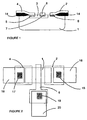
- the bipolar transistor shown in Figure 1 comprises an n-type collector region 1 which comprises the modified CMOS N-Well described below. Contact to the collector region is accomplished by the collector polysilicon electrode 2 and an N + diffusion 8 which has been driven out of the polysilicon. A shallow p-type base region 3 is provided and this is contacted by the base polysilicon electrode 4, an ohmic contact is provided by a P + region 5 formed by dopant diffused out of the base polysilicon. The emitter junction is provided by a polysilicon electrode 6 out of which the emitter N + dopant 7 has been driven.
- the three polysilicon extended electrodes can be defined at minimum geometry significantly reducing the overall device area and lowering all associated resistances and capacitances.
- Electrical contact to the device is achieved by making metallurgical contacts to the extended polysilicon electrodes where they run onto the device isolation region 14, the device size is consequently not influenced by the metal track separation and is defined purely by the polysilicon electrode separation.
- the metallurgical contacts are shown in Figure 2, identified by numerals 16,18,20.
- the metallurgical contacts are typically adhered to the polysilicon electrodes by glass contacts 15,17 and 19, shown in Figure 2.
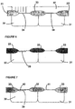
- Figure 3 shows the bipolar device of Figures 1 and 2 integrated into an existing p-type substrate CMOS structure.
- the structure includes a p-channel MOS transistor indicated generally at 20 having an N-Well 21 similar to the N-Well 1 of the bipolar transistor of Figure 1, and an n-channel MOS device 22 having a CMOS P-Well 23.
- the polysilicon electrodes 2,4,6 are shown to be the same material as the MOS gate conductor 24.
- the gate oxide 25 required for the formation of the insulating gate structure of the MOS transistor has been etched away in the bipolar device according to this invention so that the polysilicon electrodes 2,4,6 contact the silicon directly in the bipolar transistor region.
- the polysilicon electrode and the base region dopings can be achieved by utilising some of the same implants as used in the CMOS process, however, separate implants may be required for some of these stages if the implant conditions are non-optimal; this is particularly true for the emitter implant as this is a critical stage.
- Figure 4 shows the modified well structure used in the present invention.
- the doping concentration is represented on a logarithmic scale.
- the N-Well region provides both the collector (1) diffusion for the bipolar transistor and the local substrate for the p-channel MOS transistor 20.
- An optimisation of the N-Well formation process is therefore required to achieve the highest performance of the bipolar device and to maintain the existing electrical characteristics of the p-channel MOS transistor.
- the electrical characteristics of the MOS transistor will remain the same since the doping levels remain the same in the vicinity of the device active regions.
- the modified N-Well is deeper than the standard well and therefore has a lower resistance and, since this well forms the collector of the bipolar device, optimisation of the well depth will allow device performance to be maximised.
- standard MOS N-Wells would have depths of around 2 ⁇ m and surface concentrations around 5E16cm -3 whilst a modified well would have a depth nearer 3.5 ⁇ m with the same surface concentration and profile.
- the deeper well is achieved by modifying the ion implant dose and subsequent diffusion to provide the desired characteristic.
- the surface concentration may be anything between 3 x 10 16 and 1.5 x 10 17 cm -3 .
- a p-type substrate is first selected (step 1) and its surface is oxidised (step 2) to a thickness of 500 A (50 nm).
- the whole of the substrate wafer then undergoes a p-type implantation (step 3).
- the substrate surface is then masked at print step 4 and the remaining exposed area, defining the CMOS N-Well 30 undergoes n-type implantation (step 5).
- part of the p-type material defined in step 3 is "over-doped” to make it n-type.
- the resist mask laid down at step 3 is removed at step 6.
- a "well drive” (step 7) is then carried out to drive implanted material deep into the substrate. During this step a layer of oxide 2100A (210 nm) thick is grown.
- a thinner layer of oxide is grown over the substrate surface at step 9. This is the layer indicated by numeral 34 in Figure 5.
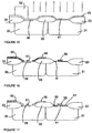
- a nitride layer 35 is deposited over the oxide (step 10) and a layer of photoresist is deposited (step 11) to mask the desired active areas (AA). Then, the nitride and oxide layers 34,35 are removed (etched) from all but the active areas (step 12) and the photoresist is then removed (step 13).
- a mask is printed to "window" the P-Well 31 and it is then implanted p-type at step 15. The resist is then stripped at step 16.
- PROCESS FLOW (1) Substrate Choice P(8-12 Ohm-cm) Epi 12 ⁇ m ⁇ 100> (2) Oxidation (500A) (3) P-Well implant (Blanket; B, 60KV,6.5E12) (4) Print N-Well (Defines CMOS and Bipolar N-Wells) (5) Implant N-Well (P,150KV,1.1E13) (6) Resist Strip (SP) (7) Well Drive (1000C,02,2100A, 1150C, N2,110m) (8) Oxide Dip (HF Dewet) (9) Pad Oxidation (250A) (10) Nitride Deposition (1500A) (11) Active Area Print (Defines MOS and Bipolar AAs) (12) Plasma Etch AA (13) Resist Strip (SP) (14) Print P
- the CMOS N-Well should have certain characteristics, particularly in terms of depth and surface concentration of dopant.
- the steps noted above are all standard CMOS technology, in the process according to the invention, particular care is taken in step 7, to achieve desired parameters, and all other steps which have an effect on the characteristics of the CMOS N-Well.
- any thin oxide which may have formed on the nitride 35 is removed in a solution of buffered hydrogen fluoride and the nitride is then removed.
- the base will next be implanted through this pad oxide into the bipolar N-Well region 30.
- the dose and energy of the base implant will have to be carefully set as the base will experience a number of high temperature processing stages (notably doping with POCL3).
- Depth and surface concentration of the base region at the end of the process will be about 1E18 (1 x 10 18 ) and 0.3 ⁇ m deep.
- Figure 6 shows a layer of photoresist 37 masking all but the base region.
- the base region is then implanted.
- the field oxide or isolation 33 acts as a mask itself so that the position of the edge of the mask 37 on the left side of Figure 6 is not critical.
- the resist is then removed, followed by the oxide 34, leaving the structure shown in Figure 7 with the base region 39 formed.
- the structure of Figure 7 is then subjected to a "pre-gate" oxidation step during which a layer of oxide 225A (22.5 nm) thick is grown onto the surface at a temperature of 920°C.
- the structure is then dipped in buffered hydrogen fluoride to remove the oxide.
- the purpose of these two steps is to remove a thin region of silicon from the substrate surface which will have been damaged during the preceding stages.
- the oxide of the isolation regions 33 is also reduced, typically to a depth of 6000A (600 nm).
- a further oxidation step is next carried out to provide a thin layer of oxide over the now "good” silicon surface, typically 200A (20 nm) thick, grown at 920°C.
- This oxide is indicated by numerals 40,41 in Figure 8.
- a standard CMOS gate oxide region 41 has now been formed, with the bipolar N-Well 30 having a base implant 39.
- the structure of Figure 8 is subjected to a threshold voltage adjustment step, that is a doping stage using boron, using a voltage of 4 keV and a dose of 1.4 x 10 12 ions per cm 2 .
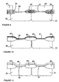
- a further printing step is carried out to define the bipolar active area, using a further mask of photoresist 43 as shown in Figure 9.
- the oxide 40 is then removed from the bipolar active area. It will be noted that the oxide 41 is left intact over the P-Well 31.
- a layer of polysilicon 45 350 nm thick is deposited over the entire substrate as shown in Figure 10.
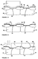
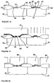
- a so-called "low temperature oxide” 46 (because it is deposited rather than being grown) is deposited over the polysilicon 45, as shown in Figure 11, a photoresist mask 47 is printed over the bipolar active area as shown in Figure 12 and the oxide 46 is etched in the region outside the mask 47 followed by removal of the photoresist, to arrive at the structure shown in Figure 13 in which an oxide layer remains over the bipolar active area.
- the exposed polysilicon is doped with POCL3.
- a deglazing step is then carried out to remove any residual POCL3 and the oxide mask 46. It will be appreciated that during this phase the mask 46 stops the POCL3 dopant from entering the bipolar region. Of course the POCL3 dopant step will sometimes not be required in which case the steps of Figure 11, 12 and 13 can be omitted.
- a mask of resist 50 has been printed to define the area of the polysilicon base electrode (see Figure 1), which is then implanted with P + dopant as shown by the arrows. Resist 50 is then removed and the reverse process is carried out as shown in Figure 15, using a further resist mask 52, to implant N + dopant into the remainder of the polysilicon layer 45.
- a printing and etching process is then carried out to define the areas of the P + base electrode 55, the N + collector electrode 56, the N + emitter electrode 57 (the emitter region is not yet formed) and the N + electrode 58 of the CMOS device.
- the lightly doped drain (LDD) regions of the CMOS device are formed by further steps of mask printing, N - implantation (Phosphorous, 70kv 2 x 10 13 ) and mask removal to define the LDD N - regions 60,61 shown in Figure 17. These are conventional CMOS process steps.
- oxide is deposited to a thickness of 2500A (250 nm) and selectively etched to provide oxide spacers 65 at the edges of all of the polysilicon electrodes 55,56,57, 58. Only some of the spacers 65 are indicated, for the sake of clarity.
- a polysilicon reoxidation process is next carried out in order to drive dopant out of the polysilicon electrodes in the bipolar region into the underlying substrate.
- the effect of this is to form an N + emitter region 69 in the P base region 39, as shown in Figure 19 and regions 66,67, equivalent to regions 5 and 8 of Figure 1.
- the reoxidation is carried out at 950°C and includes growth of an oxide layer 325A (32.5 nm) thick.
- the bipolar region is masked with resist 70 as shown in Figure 19 and then implanted with As, at 120 keV and a concentration of 5 x 10 15 , i.e. N + implantation.
- the device based on the CMOS P-Well then undergoes various standard process steps to define the CMOS device which do not form part of the invention.
- the whole device is ready for a contact printing step, comprising deposition of contact material and selective etching to leave contacts on the polysilicon electrodes, 55,56,57 (see Figure 2).
- a contact printing step comprising deposition of contact material and selective etching to leave contacts on the polysilicon electrodes, 55,56,57 (see Figure 2).
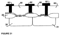
- all but the contact areas are provided with an LTO (low temperature oxide) layer 80 through which metal contacts 82 as shown in Figure 21 are provided to the electrodes 55,56,57, (not visible in Figure 21) and the N + region 60 of the PMOS device.
- the metal contacts 82 are formed by the usual steps of deposition, mask printing, etching and resist removal, followed by a final annealing step.
- Figures 22 to 24 show three variations of the transistor of Figure 1, which are within the scope of this invention. Like items in these Figures and Figure 1 are indicated with like reference numerals. Figures 22 to 24 show an oxide layer 100 formed over the polysilicon electrodes, similar to the oxide layer 80 of Figure 21.
- the common feature of Figures 22 to 24 is that instead of including three polysilicon contacts, they each have one or more metal contacts overlapping or adjacent to the polysilicon emitter contact 6 producing an extremely compact structure.
- the oxide 100 isolates the polysilicon electrodes from the metal contacts.
- the collector electrode is replaced by a metal contact 102.
- the base electrode is replaced by a metal contact 104 and in the embodiment of Figure 24 both collector and base electrodes have been replaced by metal contacts 102,104.
- the formation of the metal contacts can be achieved by the industry standard contact and metallisation procedures as used in the majority of CMOS processes.
- the bipolar transistor can use the same set of design rules provided for the CMOS device structures. In particular, standard rules that relate to the minimum spacing of structures can be adopted. The electrical characteristics of the MOS transistors are retained.
- the conductivity types of the materials can be reversed so that p-type becomes n-type and vice versa.
Landscapes
- Bipolar Transistors (AREA)
- Metal-Oxide And Bipolar Metal-Oxide Semiconductor Integrated Circuits (AREA)
- Catalysts (AREA)
- Superconductors And Manufacturing Methods Therefor (AREA)
- Amplifiers (AREA)
Claims (15)
- Transistor bipolaire formé sur un matériau possédant un premier type de conductivité, comprenant :caractérisé en ce que l'émetteur touche directement l'ensemble de la partie surjacente de l'électrode d'émetteur dans les directions tournées vers les électrodes de collecteur et de base;un puits formé d'un matériau possédant un second type de conductivité et défini par ledit substrat possédant un premier type de conductivité et formant le collecteur du transistor;une couche mince d'un matériau possédant le premier type de conductivité et formée dans la surface d'une zone sélectionnée dudit collecteur (1), formant la base (3) du transistor;une couche plus mince formée du matériau possédant le second type de conductivité et formée dans la surface d'une zone sélectionnée de ladite base (3), formant l'émetteur (7) du transistor;l'émetteur possédant une électrode en polysilicium ou en siliciure étant en contact direct avec l'émetteur et s'étendant au-delà de l'émetteur associé dans le plan du substrat,
le puits formant collecteur comporte une concentration d'atomes de dopant, qui est essentiellement uniforme depuis sa surface jusqu'à au moins 50 % de sa profondeur, puis diminue lorsque la profondeur augmente; et
le puits est en contact direct avec le matériau du substrat possédant le premier type de conductivité. - Transistor selon la revendication 1, dans lequel le puits (1) du collecteur possède une profondeur dans la gamme de 2 à 5 µm.
- Transistor selon la revendication 2, dans lequel le puits (1) du collecteur possède une profondeur supérieure à 3,5 µm.
- Transistor selon la revendication 1, 2 ou 3, dans lequel la concentration d'atomes de dopant possédant le second type de conductivité dans la surface du collecteur se situe dans la gamme allant de 3.1016 à 1,5 x 1017 cm-3.
- Transistor selon l'une quelconque des revendications précédentes, dans lequel le collecteur (1) est touché directement par une électrode en polysilicium ou en siliciure (2).
- Transistor selon l'une quelconque des revendications précédentes, dans lequel la base (3) est touchée directement par une électrode en polysilicium ou en siliciure (4).
- Circuit intégré comprenant un transistor selon l'une quelconque des revendications précédentes et comprenant en outre au moins un dispositif métal-oxyde-semiconducteur (MOS) formé dans un puits adjacent d'un matériau possédant un type de conductivité opposé, le puits possédant un second type de conductivité ayant la même profondeur et la même concentration de dopant que le puits de collecteur du transistor bipolaire.
- Procédé pour fabriquer un transistor bipolaire comprenant les étapes consistant à :définir, dans un substrat possédant un premier type de conductivité, un puits (3) possédant un second type de conductivité pour former le collecteur du transistor, dans lequel la concentration en atomes de dopant du puits (3) est essentiellement uniforme depuis sa surface jusqu'à au moins 50 % de sa profondeur, puis diminue lorsque la profondeur augmente et le collecteur est formé directement sur le substrat;masquer une zone à l'intérieur du puits pour définir une zone active du transistor et former une couche d'oxyde (33) à l'extérieur de la zone masquée;former, dans une région sélectionnée de ladite zone active, une couche mince d'un matériau possédant un premier type de conductivité pour former la région de base (39) du transistor;former une couche d'oxyde mince (40) sur le substrat, retirer l'oxyde mince de la zone active et appliquer une couche de polysilicium (45) sur l'ensemble du substrat du transistor, en contact direct avec la zone active du transistor;doper une zone du polysilicium, dont au moins une partie est située au-dessus de la région de base (39), avec le dopant possédant un second type de conductivité pour former l'électrode d'émetteur (57);retirer des zones sélectionnées du polysilicium pour définir l'électrode d'émetteur (57); etformer l'émetteur (69) du transistor en introduisant le dopant dans la région de base (39) à partir d'une partie de l'électrode d'émetteur (57) chevauchant la région de base (39).
- Procédé selon la revendication 8, dans laquelle la définition du puits comprend l'implantation d'ions dans une région sélectionnée de la surface du substrat.
- Procédé selon la revendication 9, comprenant en outre les ions implantés à diffuser dans le substrat.
- Procédé selon la revendication 8, 9 ou 10, comprenant le dopage d'une zone du polysilicium (45) dont au moins une partie recouvre la zone active à l'extérieur de la région de base, avec un dopant possédant le second type de conductivité pour former l'électrode de collecteur (56).
- Procédé selon l'une quelconque des revendications 8 à 11, consistant à doper une zone du polysilicium (45), dont au moins une partie est située au-dessus de la région de base, avec un dopant possédant le premier type de conductivité pour former une électrode de base (55).
- Procédé selon la revendication 11 ou 12, selon lequel le dopant possédant le premier type de conductivité est extrait du matériau d'électrode pour être introduit dans les régions sous-jacentes du transistor bipolaire pour former des régions de contact améliorant la conductivité depuis les régions de transistors au matériau associé de l'électrode.
- Procédé selon l'une quelconque des revendications 8 à 13, selon lequel dans chaque zone du matériau de l'électrode s'étendant au-delà de l'émetteur, du collecteur ou de la base associé dans le plan du substrat est pourvue d'un contact conducteur situé à l'extérieur de la zone active du transistor.
- Procédé pour fabriquer un circuit intégré comprenant au moins un dispositif MOS et au moins un transistor bipolaire, dans lequel les étapes de formation du dispositif MOS sont intégrées dans les étapes de formation d'un transistor bipolaire selon l'une quelconque des revendications 8 à 14, et le dispositif MOS comporte des puits adjacents formés d'un matériau ayant un type de conductivité opposée, le puits possédant le second type de conductivité du dispositif MOS étant formé simultanément en tant que puits de collecteur (30) du transistor bipolaire de manière à posséder la même profondeur et la même concentration de dopant.
Applications Claiming Priority (2)
| Application Number | Priority Date | Filing Date | Title |
|---|---|---|---|
| GB9207472 | 1992-04-06 | ||
| GB929207472A GB9207472D0 (en) | 1992-04-06 | 1992-04-06 | High performance process technology |
Publications (3)
| Publication Number | Publication Date |
|---|---|
| EP0568206A2 EP0568206A2 (fr) | 1993-11-03 |
| EP0568206A3 EP0568206A3 (en) | 1994-08-17 |
| EP0568206B1 true EP0568206B1 (fr) | 2004-03-10 |
Family
ID=10713514
Family Applications (1)
| Application Number | Title | Priority Date | Filing Date |
|---|---|---|---|
| EP93302685A Expired - Lifetime EP0568206B1 (fr) | 1992-04-06 | 1993-04-06 | Transistor bipolaire et procédé de fabrication |
Country Status (5)
| Country | Link |
|---|---|
| US (1) | US5528066A (fr) |
| EP (1) | EP0568206B1 (fr) |
| AT (1) | ATE261613T1 (fr) |
| DE (1) | DE69333446T2 (fr) |
| GB (1) | GB9207472D0 (fr) |
Families Citing this family (3)
| Publication number | Priority date | Publication date | Assignee | Title |
|---|---|---|---|---|
| JP2825169B2 (ja) * | 1990-09-17 | 1998-11-18 | キヤノン株式会社 | 半導体装置 |
| JP2008117881A (ja) * | 2006-11-02 | 2008-05-22 | Sanyo Electric Co Ltd | 半導体装置及びその製造方法 |
| US9425298B2 (en) | 2015-01-22 | 2016-08-23 | International Business Machines Corporation | Lateral bipolar transistor |
Citations (2)
| Publication number | Priority date | Publication date | Assignee | Title |
|---|---|---|---|---|
| US4120707A (en) * | 1977-03-30 | 1978-10-17 | Harris Corporation | Process of fabricating junction isolated IGFET and bipolar transistor integrated circuit by diffusion |
| US5011784A (en) * | 1988-01-21 | 1991-04-30 | Exar Corporation | Method of making a complementary BiCMOS process with isolated vertical PNP transistors |
Family Cites Families (10)
| Publication number | Priority date | Publication date | Assignee | Title |
|---|---|---|---|---|
| BE758683A (fr) * | 1969-11-10 | 1971-05-10 | Ibm | Procede de fabrication d'un dispositif monolithique auto-isolant et structure de transistor a socle |
| JPS5871655A (ja) * | 1981-10-23 | 1983-04-28 | Toshiba Corp | 半導体装置 |
| US4573256A (en) * | 1983-08-26 | 1986-03-04 | International Business Machines Corporation | Method for making a high performance transistor integrated circuit |
| US4966865A (en) * | 1987-02-05 | 1990-10-30 | Texas Instruments Incorporated | Method for planarization of a semiconductor device prior to metallization |
| JP2590236B2 (ja) * | 1987-10-07 | 1997-03-12 | 株式会社日立製作所 | 半導体装置 |
| JPH027529A (ja) * | 1988-06-27 | 1990-01-11 | Nec Corp | バイポーラトランジスタ及びその製造方法 |
| EP0405045B1 (fr) * | 1989-06-28 | 1995-12-13 | STMicroelectronics S.r.l. | Circuit intégré utilisant une technologie mixte comprenant des structures CMOS et des transistors bipolaires latéraux à haut rendement ayant une tension "early" accrue et sa fabrication |
| JPH03152939A (ja) * | 1989-11-09 | 1991-06-28 | Toshiba Corp | 半導体集積回路装置 |
| JP3126766B2 (ja) * | 1990-12-07 | 2001-01-22 | 三菱電機株式会社 | 半導体装置およびその製造方法 |
| US5358883A (en) * | 1992-02-03 | 1994-10-25 | Motorola, Inc. | Lateral bipolar transistor |
-
1992
- 1992-04-06 GB GB929207472A patent/GB9207472D0/en active Pending
-
1993
- 1993-04-06 DE DE69333446T patent/DE69333446T2/de not_active Expired - Fee Related
- 1993-04-06 EP EP93302685A patent/EP0568206B1/fr not_active Expired - Lifetime
- 1993-04-06 AT AT93302685T patent/ATE261613T1/de not_active IP Right Cessation
-
1994
- 1994-10-11 US US08/321,158 patent/US5528066A/en not_active Expired - Lifetime
Patent Citations (2)
| Publication number | Priority date | Publication date | Assignee | Title |
|---|---|---|---|---|
| US4120707A (en) * | 1977-03-30 | 1978-10-17 | Harris Corporation | Process of fabricating junction isolated IGFET and bipolar transistor integrated circuit by diffusion |
| US5011784A (en) * | 1988-01-21 | 1991-04-30 | Exar Corporation | Method of making a complementary BiCMOS process with isolated vertical PNP transistors |
Also Published As
| Publication number | Publication date |
|---|---|
| GB9207472D0 (en) | 1992-05-20 |
| DE69333446D1 (de) | 2004-04-15 |
| ATE261613T1 (de) | 2004-03-15 |
| US5528066A (en) | 1996-06-18 |
| EP0568206A3 (en) | 1994-08-17 |
| DE69333446T2 (de) | 2005-01-20 |
| EP0568206A2 (fr) | 1993-11-03 |
Similar Documents
| Publication | Publication Date | Title |
|---|---|---|
| CA1194612A (fr) | Methode d'apport de dispositifs complementaires sur circuits integres | |
| US5468666A (en) | Using a change in doping of poly gate to permit placing both high voltage and low voltage transistors on the same chip | |
| EP0749165B1 (fr) | Transitor à couche mince sur un substrat semi-conducteur isolé et méthode de fabrication | |
| US6277675B1 (en) | Method of fabricating high voltage MOS device | |
| US4752589A (en) | Process for the production of bipolar transistors and complementary MOS transistors on a common silicon substrate | |
| US4475279A (en) | Method of making a monolithic integrated circuit comprising at least one pair of complementary field-effect transistors and at least one bipolar transistor | |
| EP0139019B1 (fr) | Dispositif semiconducteur et son procede de fabrication | |
| EP0676810A2 (fr) | Transistor à effet de champ à grille isolée et procédé de fabrication | |
| US4849364A (en) | Semiconductor devices | |
| EP0676798A2 (fr) | Dispositif à effet de champ à grille isolée avec canal asymétrique et méthode de manufacture | |
| CN116487381A (zh) | 中高压mos器件及其版图结构和制造方法 | |
| KR0166052B1 (ko) | 고전압 병합 바이폴라/cmos 및 그 제조 방법 | |
| US4784966A (en) | Self-aligned NPN bipolar transistor built in a double polysilicon CMOS technology | |
| US6583013B1 (en) | Method for forming a mixed voltage circuit having complementary devices | |
| US5005066A (en) | Self-aligned NPN bipolar transistor built in a double polysilicon CMOS technology | |
| KR890004797B1 (ko) | 우물영역을 갖는 반도체기판상에 형성되는 mis형 반도체장치 | |
| JP2587444B2 (ja) | Cmos技術を用いたバイポーラ・トランジスタとその製造方法 | |
| US6083795A (en) | Large angle channel threshold implant for improving reverse narrow width effect | |
| US4547959A (en) | Uses for buried contacts in integrated circuits | |
| KR930005508B1 (ko) | 반도체장치 및 그 제조방법 | |
| US5528066A (en) | Bipolar transistor having a collector well with a particular concentration | |
| US7560779B2 (en) | Method for forming a mixed voltage circuit having complementary devices | |
| US5994190A (en) | Semiconductor device with impurity layer as channel stopper immediately under silicon oxide film | |
| EP0348626B1 (fr) | Procédé pour l'intégration de transistors isolés bipolaires verticaux et JFET et circuit intégré correspondant | |
| JP2578662B2 (ja) | 半導体装置の製造方法 |
Legal Events
| Date | Code | Title | Description |
|---|---|---|---|
| PUAI | Public reference made under article 153(3) epc to a published international application that has entered the european phase |
Free format text: ORIGINAL CODE: 0009012 |
|
| AK | Designated contracting states |
Kind code of ref document: A2 Designated state(s): AT BE CH DE ES FR GB IE IT LI NL SE |
|
| PUAL | Search report despatched |
Free format text: ORIGINAL CODE: 0009013 |
|
| AK | Designated contracting states |
Kind code of ref document: A3 Designated state(s): AT BE CH DE ES FR GB IE IT LI NL SE |
|
| 17P | Request for examination filed |
Effective date: 19950203 |
|
| 17Q | First examination report despatched |
Effective date: 19961122 |
|
| REG | Reference to a national code |
Ref country code: GB Ref legal event code: FG4D |
|
| GRAP | Despatch of communication of intention to grant a patent |
Free format text: ORIGINAL CODE: EPIDOSNIGR1 |
|
| GRAS | Grant fee paid |
Free format text: ORIGINAL CODE: EPIDOSNIGR3 |
|
| GRAA | (expected) grant |
Free format text: ORIGINAL CODE: 0009210 |
|
| RAP1 | Party data changed (applicant data changed or rights of an application transferred) |
Owner name: TEXAS INSTRUMENTS LIMITED |
|
| AK | Designated contracting states |
Kind code of ref document: B1 Designated state(s): AT BE CH DE ES FR GB IE IT LI NL SE |
|
| PG25 | Lapsed in a contracting state [announced via postgrant information from national office to epo] |
Ref country code: NL Free format text: LAPSE BECAUSE OF FAILURE TO SUBMIT A TRANSLATION OF THE DESCRIPTION OR TO PAY THE FEE WITHIN THE PRESCRIBED TIME-LIMIT Effective date: 20040310 Ref country code: LI Free format text: LAPSE BECAUSE OF FAILURE TO SUBMIT A TRANSLATION OF THE DESCRIPTION OR TO PAY THE FEE WITHIN THE PRESCRIBED TIME-LIMIT Effective date: 20040310 Ref country code: IT Free format text: LAPSE BECAUSE OF FAILURE TO SUBMIT A TRANSLATION OF THE DESCRIPTION OR TO PAY THE FEE WITHIN THE PRE;WARNING: LAPSES OF ITALIAN PATENTS WITH EFFECTIVE DATE BEFORE 2007 MAY HAVE OCCURRED AT ANY TIME BEFORE 2007. THE CORRECT EFFECTIVE DATE MAY BE DIFFERENT FROM THE ONE RECORDED.SCRIBED TIME-LIMIT Effective date: 20040310 Ref country code: CH Free format text: LAPSE BECAUSE OF FAILURE TO SUBMIT A TRANSLATION OF THE DESCRIPTION OR TO PAY THE FEE WITHIN THE PRESCRIBED TIME-LIMIT Effective date: 20040310 Ref country code: BE Free format text: LAPSE BECAUSE OF FAILURE TO SUBMIT A TRANSLATION OF THE DESCRIPTION OR TO PAY THE FEE WITHIN THE PRESCRIBED TIME-LIMIT Effective date: 20040310 Ref country code: AT Free format text: LAPSE BECAUSE OF FAILURE TO SUBMIT A TRANSLATION OF THE DESCRIPTION OR TO PAY THE FEE WITHIN THE PRESCRIBED TIME-LIMIT Effective date: 20040310 |
|
| RIC1 | Information provided on ipc code assigned before grant |
Ipc: 7H 01L 29/41 B Ipc: 7H 01L 21/82 B Ipc: 7H 01L 27/06 A |
|
| REG | Reference to a national code |
Ref country code: CH Ref legal event code: EP |
|
| PG25 | Lapsed in a contracting state [announced via postgrant information from national office to epo] |
Ref country code: IE Free format text: LAPSE BECAUSE OF NON-PAYMENT OF DUE FEES Effective date: 20040406 |
|
| REG | Reference to a national code |
Ref country code: IE Ref legal event code: FG4D |
|
| REF | Corresponds to: |
Ref document number: 69333446 Country of ref document: DE Date of ref document: 20040415 Kind code of ref document: P |
|
| PG25 | Lapsed in a contracting state [announced via postgrant information from national office to epo] |
Ref country code: SE Free format text: LAPSE BECAUSE OF FAILURE TO SUBMIT A TRANSLATION OF THE DESCRIPTION OR TO PAY THE FEE WITHIN THE PRESCRIBED TIME-LIMIT Effective date: 20040610 |
|
| PG25 | Lapsed in a contracting state [announced via postgrant information from national office to epo] |
Ref country code: ES Free format text: LAPSE BECAUSE OF FAILURE TO SUBMIT A TRANSLATION OF THE DESCRIPTION OR TO PAY THE FEE WITHIN THE PRESCRIBED TIME-LIMIT Effective date: 20040621 |
|
| NLV1 | Nl: lapsed or annulled due to failure to fulfill the requirements of art. 29p and 29m of the patents act | ||
| REG | Reference to a national code |
Ref country code: CH Ref legal event code: PL |
|
| ET | Fr: translation filed | ||
| PLBE | No opposition filed within time limit |
Free format text: ORIGINAL CODE: 0009261 |
|
| STAA | Information on the status of an ep patent application or granted ep patent |
Free format text: STATUS: NO OPPOSITION FILED WITHIN TIME LIMIT |
|
| REG | Reference to a national code |
Ref country code: IE Ref legal event code: MM4A |
|
| 26N | No opposition filed |
Effective date: 20041213 |
|
| PGFP | Annual fee paid to national office [announced via postgrant information from national office to epo] |
Ref country code: DE Payment date: 20080430 Year of fee payment: 16 |
|
| PGFP | Annual fee paid to national office [announced via postgrant information from national office to epo] |
Ref country code: FR Payment date: 20080403 Year of fee payment: 16 |
|
| PGFP | Annual fee paid to national office [announced via postgrant information from national office to epo] |
Ref country code: GB Payment date: 20090312 Year of fee payment: 17 |
|
| REG | Reference to a national code |
Ref country code: FR Ref legal event code: ST Effective date: 20091231 |
|
| PG25 | Lapsed in a contracting state [announced via postgrant information from national office to epo] |
Ref country code: DE Free format text: LAPSE BECAUSE OF NON-PAYMENT OF DUE FEES Effective date: 20091103 |
|
| PG25 | Lapsed in a contracting state [announced via postgrant information from national office to epo] |
Ref country code: FR Free format text: LAPSE BECAUSE OF NON-PAYMENT OF DUE FEES Effective date: 20091222 |
|
| GBPC | Gb: european patent ceased through non-payment of renewal fee |
Effective date: 20100406 |
|
| PG25 | Lapsed in a contracting state [announced via postgrant information from national office to epo] |
Ref country code: GB Free format text: LAPSE BECAUSE OF NON-PAYMENT OF DUE FEES Effective date: 20100406 |