EP0568221A1 - Procédé et dispositif de mise en oeuvre d'un schéma de remplacement pseudo-LRU avec une fonction verrouillage - Google Patents
Procédé et dispositif de mise en oeuvre d'un schéma de remplacement pseudo-LRU avec une fonction verrouillage Download PDFInfo
- Publication number
- EP0568221A1 EP0568221A1 EP93302988A EP93302988A EP0568221A1 EP 0568221 A1 EP0568221 A1 EP 0568221A1 EP 93302988 A EP93302988 A EP 93302988A EP 93302988 A EP93302988 A EP 93302988A EP 0568221 A1 EP0568221 A1 EP 0568221A1
- Authority
- EP
- European Patent Office
- Prior art keywords
- cache
- memory
- line
- lock
- bit
- Prior art date
- Legal status (The legal status is an assumption and is not a legal conclusion. Google has not performed a legal analysis and makes no representation as to the accuracy of the status listed.)
- Granted
Links
Images


Classifications
-
- G—PHYSICS
- G06—COMPUTING OR CALCULATING; COUNTING
- G06F—ELECTRIC DIGITAL DATA PROCESSING
- G06F12/00—Accessing, addressing or allocating within memory systems or architectures
- G06F12/02—Addressing or allocation; Relocation
- G06F12/08—Addressing or allocation; Relocation in hierarchically structured memory systems, e.g. virtual memory systems
- G06F12/12—Replacement control
- G06F12/121—Replacement control using replacement algorithms
- G06F12/126—Replacement control using replacement algorithms with special data handling, e.g. priority of data or instructions, handling errors or pinning
-
- G—PHYSICS
- G06—COMPUTING OR CALCULATING; COUNTING
- G06F—ELECTRIC DIGITAL DATA PROCESSING
- G06F12/00—Accessing, addressing or allocating within memory systems or architectures
- G06F12/02—Addressing or allocation; Relocation
- G06F12/08—Addressing or allocation; Relocation in hierarchically structured memory systems, e.g. virtual memory systems
- G06F12/12—Replacement control
-
- G—PHYSICS
- G06—COMPUTING OR CALCULATING; COUNTING
- G06F—ELECTRIC DIGITAL DATA PROCESSING
- G06F13/00—Interconnection of, or transfer of information or other signals between, memories, input/output devices or central processing units
- G06F13/14—Handling requests for interconnection or transfer
-
- G—PHYSICS
- G06—COMPUTING OR CALCULATING; COUNTING
- G06F—ELECTRIC DIGITAL DATA PROCESSING
- G06F12/00—Accessing, addressing or allocating within memory systems or architectures
- G06F12/02—Addressing or allocation; Relocation
- G06F12/08—Addressing or allocation; Relocation in hierarchically structured memory systems, e.g. virtual memory systems
- G06F12/12—Replacement control
- G06F12/121—Replacement control using replacement algorithms
- G06F12/123—Replacement control using replacement algorithms with age lists, e.g. queue, most recently used [MRU] list or least recently used [LRU] list
- G06F12/125—Replacement control using replacement algorithms with age lists, e.g. queue, most recently used [MRU] list or least recently used [LRU] list being generated by decoding an array or storage
Definitions
- This invention relates to the field of computer cache memory devices. More particularly, the present invention relates to a method and apparatus for "locking" data into the cache memory such that a program can designate pages or blocks of memory which should remain in the cache.
- a simple way to increase the throughput of a computer processor is to increase the frequency of the clock driving the processor.
- the processor may begin to exceed the speed at which the main memory can respond to the processor's requests.
- the processor may therefore be forced to wait for the main memory to respond.
- cache memory was created.
- Cache memory refers to a small amount of high-speed memory that is coupled closely to the processor.
- the cache memory is used to duplicate a subset of main memory locations.
- a processor When a processor needs data from memory, it will first look into the high-speed cache memory. If the data is found in the cache memory (known as a "hit"), the data will be retrieved from the cache memory and execution will resume. If the data is not found in the cache memory (known as a "miss”) then the processor will proceed to look into the slower main memory.
- a particular program will refer to a particular data table in the main memory often, it would be desirable to place a copy of the data table into a high-speed cache memory. If a copy of the data table is kept in the cache memory, then each time the processor needs data from the data table it will be retrieved quickly.
- Cache memories usually store only a small subset of the main memory. When every location in the cache memory is filled, the cache memory must discard some of the data from what is currently in store. Determining which memory cache locations to discard is a difficult task since it is often not known which cache memory locations will be needed in the future. Various heuristics have been developed to aid in determining which main memory locations will be duplicated in the high-speed cache memory.
- FIG. 1 a high level block diagram of a prior art cache memory system is shown.
- the main memory 10, cache memory system 12 and processor 14 are coupled in a bus 16.
- the processor issues memory requests to the cache memory system 12. If the information is available in the cache memory 15 the information requested is immediately forwarded to processor 14 via a dedicated line 18. If the information is not located in the cache memory 15, the request is forwarded to the slower main memory 10, which provides the information requested to processor 14 via the bus 16.
- any block of main memory can be represented in any cache memory line.
- each block of main memory can be represented in only one particular cache memory location.
- each block of main memory can only be placed into cache memory lines having the same set number.
- the cache controller In order to control the operation of the cache memory, there is dedicated control logic referred to as the cache controller (17, Figure 1).
- a table is located within the cache controller.
- the TAG table is used for storing information used for mapping main memory physical addresses into a cache memory set and line address.
- the TAG table stores block address and related control bits for each cache memory line.
- the block address refers to the physical main memory block address that is currently represented in the cache memory line.
- the control bits store information such as whether or not the cache memory line has valid data.
- the table stores data utilized to implement a cache replacement algorithm. The data table is divided to match the organization of the cache memory.
- the cache controller When all the lines in a cache memory set become full and a new block of memory needs to be placed into the cache memory, the cache controller must discard the contents of part of the cache memory and replace it with the new data from main memory. Preferably, the contents of the cache memory line discarded will not be needed in the near future. However, the cache controller can only predict which cache memory line should be discarded. As briefly noted earlier, in order to predict as efficiently as possible, several cache replacement heuristics have been developed. The presently used cache replacement heuristics include Round-Robin, Random, Least-Recently-Used (LRU), and Pseudo-Least-Recently-Used. These heuristics determine which cache memory location to replace by looking only at the cache memory's past performance.
- the Round-Robin replacement heuristic simply replaces the cache memory lines in a sequential order. When the last cache memory line is reached, then the controller starts back at the first cache memory line.
- the Least-Recently-Used (LRU) replacement scheme requires more intelligence at the cache controller.
- LRU the assumption is that when a cache memory line has been accessed recently, it will most likely be accessed again in the near future. Based upon this assumption, then the cache memory line that that has been "least recently used" should be replaced by the cache controller.
- the cache controller To implement the LRU heuristic, the cache controller must mark each cache memory line with a time counter each time there is a "hit" on that cache memory line. When the cache controller is forced to replace a cache memory line, the cache controller replaces the cache memory line with the oldest time counter value. In this manner the cache memory line which was "least recently used" will be replaced.
- the LRU heuristic is relatively efficient, it does have drawbacks.
- One problem with the LRU replacement scheme is that it wastes valuable high-speed cache memory. Each time a cache hit occurs, the cache controller must place a time counter value in memory location associated with the cache memory line.
- Another problem with the LRU replacement scheme is that it requires complex logic to implement. When a replacement must occur, the cache controller must compare all the cache memory line time counter values, this procedure wastes valuable time. When these factors are accounted for, the LRU scheme loses some of its efficiency.
- the Pseudo-Least-Recently-Used (PLRU) replacement scheme is somewhat similar to the LRU replacement scheme except that it requires less complex logic and does not require much high-speed cache memory to implement. However, since the PLRU scheme employs shortcuts to speed up operation, the least recently accessed cache memory location is not always the location replaced.
- each cache memory line is assigned an MRU (or Most-Recently-Used) bit which is stored in the TAG table.
- the MRU bit for each cache memory line is set to a "1" each time a "hit" occurs on the cache memory line. Thus, a "1" in the MRU bit indicates that the cache memory line has been used recently.
- the cache controller When the cache controller is forced to replace a cache memory line, the cache controller examines the MRU bits for each cache memory line looking for a "0". If the MRU bit for a particular cache memory line is set to a "1", then the cache controller does not replace that cache memory line since it was used recently. When the cache controller finds a memory line with the MRU bit set to "0", that memory line is replaced and the MRU bit associated with the cache memory line is then set to "1".
- the PLRU scheme is best explained by the use of an example. Referring to Figure 2 , an example of the PLRU replacement scheme is illustrated in a cache environment with 4 cache tines available.
- all the MRU bits are cleared indicating that none of the cache lines have been used recently and all the cache lines are free for replacement.
- a cache hit occurs on the data in line 3.
- the cache controller causes the MRU bit for line 3 to be set to "1", indicating that the data in line 3 has been used recently. Cache lines 0, 1, and 2 are still available.
- a cache hit occurs on the data in line 1.
- the cache controller causes the MRU bit for line 1 to be set to "1", indicating that the data in line 1 has been used recently.
- a cache hit occurs on the data in line 0.
- the cache controller similarly causes the MRU bit for line 0 to be set to "1", indicating that the data in line 0 has been used recently. Now, only Cache line 2 has not been marked as being used recently.
- a cache hit occurs on the data in line 2. If the MRU bit for line 2 is set to a "1", all the MRU bits would be set to "1 " (1111) and no cache lines would be available for replacement. This would be a case of cache deadlock. Instead, the cache controller causes all of the MRU bits to be cleared and sets the MRU bit for line 2 to a "1". Now lines 0, 1, and 3 are available for replacement. The act of clearing of all the MRU bits results in the loss of some cache history, but is required in order to avoid cache deadlock. The cache operations then continue as before.
- these heuristics can be improved if some information is known about the cache memory's future usage. For example, if it is known that a certain cache memory location will be used in the near future, it would be best not replace that cache memory location. In the example given earlier, it was known that the program would access the data in the data table repeatedly. If the data table was placed into the cache memory in that case, it would be advantageous to be able to "lock" that cache memory location so that it could not be replaced. If this was done, then each time the program subsequently needed information from the data table it would always be found in the cache memory. Therefore, the data in the data table would always be quickly fetched from the cache memory instead of having to be retrieved from the slower main memory.
- the method and apparatus of the present invention comprises a cache memory replacement scheme which utilizes locking bits. These locking bits are preferably set and reset by the application program/process executing and are utilized in conjunction with cache replacement bits by the cache controller to determine the lines in the cache to replace. The locking bits "lock" the line of data in the cache until such time when the process resets the lock bit.
- FIGURE 1 is a high-level block diagram of a typical prior art cache memory system.
- FIGURE 2 illustrates an exemplary prior art pseudo-least-recently-used replacement process.
- FIGURE 3 illustrates a prior art set associative cache.
- FIGURES 4a, 4b and 4c illustrate a preferred embodiment of the cache system of the present invention and the locking bits employed.
- FIGURE 5 illustrates the STAG and PTAG tables utilized in the preferred embodiment of the cache system of the present invention.
- FIGURE 6 illustrates a pseudo-least-recently-used replacement process employing locking bits.
- a cache which implements a least recently used replacement algorithm is provided with the ability to lock certain memory locations in the cache. If a memory location in the cache is locked, the information contained therein remains in the cache until the lock is removed and the cache replacement algorithm determines that the line of the cache should be replaced.
- the tag table is provided with an additional bit, a lock bit, which is associated with each line of cache memory. Preferably this bit can be set by the process accessing that particular cache memory location.
- a lock bit which is associated with each line of cache memory. Preferably this bit can be set by the process accessing that particular cache memory location.
- the present invention has been implemented using the set associative mapping system and a pseudo-least-recently-used replacement algorithm.
- the cache system of the present invention is not limited to cache memory systems with set associative mapping or to the pseudo-least-recently-used replacement algorithm.
- FIG. 3 a block diagram of a set exemplary of associative cache memory is shown.
- each set is given a label from 0 to 63.
- Each set in the cache memory contains 4 "lines” of cache memory.
- Each line of cache memory in each set is given a label 0 through 3.
- Each cache memory line is capable of storing an entire "block" of main memory.
- the main memory is also divided into a number of sets.
- the number of sets that the main memory is divided into is equal to the number of sets in the cache memory.
- the main memory is divided into 64 sets.
- the main memory is divided up according to the high order bits of the block address.
- the sets could just as easily be divided using the low order bits of the block address such that all block addresses which end in 0 belong in set 0, and all block addresses which end in 1 belong to set 1.
- set 0 encompasses blocks 0, N, 2N ... 61N, 62N, 63N
- set 1 encompasses blocks 1, N+1, 2N+1 ... 61N+1, 62N+1, 63N+1.
- the main memory sets are considerably larger than the cache memory sets.
- Each set of main memory is then further divided into a number of memory blocks.
- Each block of main memory can only by duplicated in the cache memory having the same set number. For example, block 3 in set 0 can only be duplicated in set 0 of the cache memory and block n+1 in set 1 can only be duplicated in set 1 of cache memory.
- each set of cache memory is made up of a number of “lines” of cache memory.
- the “lines” of cache memory are equal in size to the “blocks” of main memory and are used for storing duplicates of main memory blocks.
- cache memory lines and main memory blocks are the same, except that "lines” only exist in the cache memory and blocks only exist in the main memory.
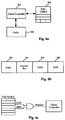
- FIG. 4a shows cache 300 which contains the memory contents of addresses most recently accessed.
- Cache controller 310 controls the access to the cache 300 and implements the cache replacement algorithm to update the cache.
- the tag table 315 contains information regarding the memory or tag address of the data contained in the cache as well as control bits.
- FIG 4b an illustrative entry in the tag table is shown.
- One tag table entry is provided for each line in the cache.
- each entry is provided with a bit MRU 335 which is set when the cache at that particular line is accessed. This is utilized in the replacement algorithm implemented by the cache controller.
- a lock bit 340 is provided to prevent the line in the cache from being replaced.
- This lock bit is settable by the processor program accessing the cache and is similarly, resettable by that program when repeated access to that information is no longer required and the line in the cache can be replaced.
- the concept may be visualized by reference to Figure 4c .
- the cache controller accesses the tag table to read the MRU and lock data.
- the lock data and MRU data may be logically ORed together to result in the replace bit indicative of whether that particular line in the cache can be replaced.
- This logical OR function may be performed by the cache controller itself or by external logic.
- the OR function result is known as the Composite Mask. If the resultant replace bit in the Composite Mask is set, the line in the cache is not removed for replacement by a different memory location. Thus, regardless of the value of the MRU bit, the lock bit can be set to ensure that the data is maintained in the cache.
- the tag table is implemented as two separate tag tables as shown in Figure 5 .
- the first table PTAG 400 comprises the address information and control bits.
- the address refers to the physical main memory block address that is currently represented in the cache memory line.
- Control bits include a valid bit which indicates if the cache memory line contains valid data.
- a second table STAG 410 is provided.
- the STAG contains the MRU bits and the lock bits for each line of cache memory. As noted earlier, the MRU bit is used for implementing a Pseudo-Least-Recently-Used replacement scheme.
- the cache controller monitors the state of the composite mask to ensure that the composite mask never reaches the state where all the composite bits for all lines are set and cache deadlock occurs.
- a mechanism is provided to monitor the number of lock bits set and to inhibit additional lock requests by an application program if a predetermined number of lock bits are set.
- the mechanism may be provided in the cache controller, the program/process or compiler. Alternately, to avoid the locking of all cache lines, it is preferred that cache memory line 0 is controlled such that the lock bit is never set. This provides a simple low overhead solution to the problem and avoids deadlocks due to programmer errors.
- step 6 a sample use of the replacement scheme of the present invention is given.
- all the MRU bits and lock bits are cleared.
- step 2 a cache hit occurs on the data in line 3.
- the cache controller causes the MRU bit for cache memory line 3 to be set to "1", indicating that the data in line 3 has been used recently. Cache lines 0, 1, and 2 are still available.
- step 3 the user program locks the data located at line 2.
- the cache controller sets the lock bit for cache memory line 2 to "1", indicating that the data in line 2 is now locked into the cache.
- the composite mask, created by the logical "OR” of the MRU bits and the lock bits is "1100", indicate that cache lines 0 and 1 are still available.
- step 4 a hit occurs on the data in line 2.
- the cache controller causes the MRU bit for cache memory line 2 to be set to "1", indicating that the data in line 2 has been used recently.
- This composite mask remains "1100", indicating that cache lines 0 and 1 are still available.
- step 5 a hit occurs on the data located at line 0.
- the cache controller causes the MRU bit for cache memory line 0 to be set to "1", indicating that the data in line 0 has been used recently.
- the resultant composite mask is "1101” indicating that only line 1 remains available for replacement.
- step 6 a hit occurs on the data in line 1. If the cache controller causes the MRU bit to be set to "1", the composite mask would be "1111". Instead, the cache controller causes the MRU bits to be reset and the MRU bit for cache memory line 1 to be set to "1", indicating that the data in line 1 has been used recently. The resultant composite mask is now "0110" as the lock bit for line 2 remains set.
- step 7 the user program executes an instruction to lock the data in line 3. The cache controller carries out this instruction by causing the lock bit for line 3 to be set to "1". In step 8, a cache hit occurs on line 0. Again, the cache controller must clear the MRU bits to prevent a composite mask of "1111" from occurring. In step 9, the user locks cache memory line 1.
- step 11 a cache hit occurs on line 1.
- the MRU bit for line 1 is set to "1" indicating that it has been used recently. Still, only cache memory line 0 is available.
- step 12 the user finally unlocks the cache memory line 2 by unlocking line 2.
- the composite mask now becomes “1010", indicating that lines 0 and 2 are now available for replacement.
- step 13 when a hit occurs on line 0, the MRU bit for line 0 is set to "1". Unlike step 10, the setting of line 0's MRU bit will now not cause deadlock because additional lines have been unlocked.
- a distinctive advantage gained by utilizing the locking mechanism in the cache system of the present invention is the added intelligence provided to the cache replacement process.
- the lock bits are set by the application process thereby eliminating the intelligence required to try to provide that knowledge at the cache controller level.
- One way to provide the request to lock certain cache memory lines is for the application program to program such request into the application program in the form of a predetermined command or subroutine call. If the programmer knows that certain variables or memory locations are to be accessed frequently during the execution of the program, after the first access, a special command may be issued to set the corresponding lock bit. The compiler compiling this program will recognize the command request and provide the proper code to execute the command.
- System Programs such as operating system routines, some database or window system routines may be used for controlling the locking as set forth in the present invention. Locking performed in the system programs boosts the performance of some key features used by application programs without any intervention from the application programmer. For example, a programmer building a graphics package might use an efficient line drawing function provided by the operating system's graphics library. If this function were locked into the cache, the speed of execution of the graphics package can be indirectly increased.
- the locking mechanism of the present invention has been provided for use through special assembly language instructions available for execution in supervisor mode only.
- a system call providing the lock and unlock line commands can easily be written to help a programmer. This is a very powerful mechanism and should be used by a knowledgeable programmer only.
- SPARCTM SPARC is a trademark of SPARC International, Inc.
- a load/store instruction can be adapted to modify the lock bits.
- One way to adapt the load/store command is by reserving an ASI value to correspond to the location of the lock bits.
- the cache controller receives a command from the CPU to unlock/lock certain lock bits.
- the cache controller responds by issuing a command to set/reset specified lock bits in the tag array.
- the SPARC Architecture Manual Version 8, pp. 45-49 (Prentiss Hall 1992).
- intelligent compilers are provided that perform an automated analysis on the memory accesses to be performed to determine those memory accesses of high frequency which would benefit by having the corresponding lock bit set. A command can then be automatically inserted into the compiled code to perform the locking and subsequently, the unlocking of the lock bits.
- This technique is advantageous as the decision whether to lock certain accesses in the cache is automatically determined by the compiler and would release the application programmer from making such a decision.
- Cache systems implementing the PLRU with locking feature as described above can exhibit significantly lower cache memory miss rates than ordinary PLRU cache systems.
- the gained efficiency is due to the "intelligence" added to the cache replacement heuristic.
Landscapes
- Engineering & Computer Science (AREA)
- Theoretical Computer Science (AREA)
- Physics & Mathematics (AREA)
- General Engineering & Computer Science (AREA)
- General Physics & Mathematics (AREA)
- Memory System Of A Hierarchy Structure (AREA)
Applications Claiming Priority (2)
| Application Number | Priority Date | Filing Date | Title |
|---|---|---|---|
| US07/875,357 US5353425A (en) | 1992-04-29 | 1992-04-29 | Methods and apparatus for implementing a pseudo-LRU cache memory replacement scheme with a locking feature |
| US875357 | 1992-04-29 |
Publications (2)
| Publication Number | Publication Date |
|---|---|
| EP0568221A1 true EP0568221A1 (fr) | 1993-11-03 |
| EP0568221B1 EP0568221B1 (fr) | 1998-12-23 |
Family
ID=25365663
Family Applications (1)
| Application Number | Title | Priority Date | Filing Date |
|---|---|---|---|
| EP93302988A Expired - Lifetime EP0568221B1 (fr) | 1992-04-29 | 1993-04-19 | Procédé et dispositif de mise en oeuvre d'un schéma de remplacement pseudo-LRU avec une fonction verrouillage |
Country Status (5)
| Country | Link |
|---|---|
| US (1) | US5353425A (fr) |
| EP (1) | EP0568221B1 (fr) |
| JP (1) | JPH0619797A (fr) |
| KR (1) | KR100293276B1 (fr) |
| DE (1) | DE69322683T2 (fr) |
Cited By (17)
| Publication number | Priority date | Publication date | Assignee | Title |
|---|---|---|---|---|
| DE4407626C1 (de) * | 1994-03-08 | 1995-05-24 | Karl Michael Marks | Verfahren und Einrichtung zur Steuerung der Datenverfügbarkeit in Zwischenspeichern bei Computern |
| EP0687979A1 (fr) * | 1994-06-14 | 1995-12-20 | Kabushiki Kaisha Toshiba | Antémémoire à inscription verrouillable |
| WO1998002818A1 (fr) * | 1996-07-16 | 1998-01-22 | Advanced Micro Devices, Inc. | Unite memoire de donnees concue pour le stockage de donnees en un seul site d'horloge et procede de fonctionnement de cette unite |
| US5761712A (en) * | 1995-06-07 | 1998-06-02 | Advanced Micro Devices | Data memory unit and method for storing data into a lockable cache in one clock cycle by previewing the tag array |
| EP0768608A3 (fr) * | 1995-10-13 | 1998-08-12 | Sun Microsystems, Inc. | Antémémoire à consultation simultanée maximale pour des systèmes d'ordinateurs à environnement à fils multiples |
| WO1999023567A1 (fr) * | 1997-10-31 | 1999-05-14 | Koninklijke Philips Electronics N.V. | Politique de remplacement d'antememoire avec verrouillage |
| WO2000077820A3 (fr) * | 1999-06-15 | 2001-06-28 | Sun Microsystems Inc | Dispositif de mise en place de pages pour systeme d'exploitation, permettant de maximiser la reutilisation des donnees de memoire cache |
| EP1089185A3 (fr) * | 1999-10-01 | 2001-09-19 | Fujitsu Limited | Procédé de commande d'une antémémoire pour augmenter la vitesse d'accès à une mémoire principale et ordinateur utilisant ce procédé |
| US6732234B1 (en) | 2000-08-07 | 2004-05-04 | Broadcom Corporation | Direct access mode for a cache |
| US6748495B2 (en) | 2001-05-15 | 2004-06-08 | Broadcom Corporation | Random generator |
| US6748492B1 (en) | 2000-08-07 | 2004-06-08 | Broadcom Corporation | Deterministic setting of replacement policy in a cache through way selection |
| GB2374178B (en) * | 1999-12-30 | 2004-08-25 | Intel Corp | A method and apparatus to perform a round robin and locking cache replacement scheme |
| AT500858B1 (de) * | 2004-08-17 | 2006-04-15 | Martin Schoeberl | Instruction cache für echtzeitsysteme |
| US7502887B2 (en) | 2003-11-12 | 2009-03-10 | Panasonic Corporation | N-way set associative cache memory and control method thereof |
| US7827360B2 (en) | 2007-08-02 | 2010-11-02 | Freescale Semiconductor, Inc. | Cache locking device and methods thereof |
| US9195625B2 (en) | 2009-10-29 | 2015-11-24 | Freescale Semiconductor, Inc. | Interconnect controller for a data processing device with transaction tag locking and method therefor |
| US9251080B2 (en) | 2009-11-30 | 2016-02-02 | International Business Machines Corporation | Managing processor thread access to cache memory using lock attributes |
Families Citing this family (120)
| Publication number | Priority date | Publication date | Assignee | Title |
|---|---|---|---|---|
| US5974508A (en) * | 1992-07-31 | 1999-10-26 | Fujitsu Limited | Cache memory system and method for automatically locking cache entries to prevent selected memory items from being replaced |
| JPH06243036A (ja) * | 1993-02-12 | 1994-09-02 | Hitachi Ltd | キャッシュ制御システム |
| JPH06282488A (ja) * | 1993-03-25 | 1994-10-07 | Mitsubishi Electric Corp | キャッシュ記憶装置 |
| US5778424A (en) * | 1993-04-30 | 1998-07-07 | Avsys Corporation | Distributed placement, variable-size cache architecture |
| JP3230898B2 (ja) * | 1993-06-02 | 2001-11-19 | シャープ株式会社 | データ駆動型情報処理システム |
| US5526511A (en) * | 1993-12-23 | 1996-06-11 | Unisys Corporation | Enhanced least recently used round robin cache management method and apparatus for allocation and destaging of cache segments |
| US5809527A (en) * | 1993-12-23 | 1998-09-15 | Unisys Corporation | Outboard file cache system |
| US5809524A (en) * | 1994-01-04 | 1998-09-15 | Intel Corporation | Method and apparatus for cache memory replacement line identification |
| TW243509B (en) * | 1994-01-31 | 1995-03-21 | Ibm | Data processor with memory cache and method of operation |
| JPH07334310A (ja) * | 1994-06-06 | 1995-12-22 | Toshiba Corp | ディスク装置及び同装置における読み出しデータのバッファ記憶制御方法 |
| US5548742A (en) * | 1994-08-11 | 1996-08-20 | Intel Corporation | Method and apparatus for combining a direct-mapped cache and a multiple-way cache in a cache memory |
| US5613153A (en) * | 1994-10-03 | 1997-03-18 | International Business Machines Corporation | Coherency and synchronization mechanisms for I/O channel controllers in a data processing system |
| US5890221A (en) * | 1994-10-05 | 1999-03-30 | International Business Machines Corporation | Method and system for offset miss sequence handling in a data cache array having multiple content addressable field per cache line utilizing an MRU bit |
| US5594886A (en) * | 1994-10-23 | 1997-01-14 | Lsi Logic Corporation | Pseudo-LRU cache memory replacement method and apparatus utilizing nodes |
| US6170047B1 (en) | 1994-11-16 | 2001-01-02 | Interactive Silicon, Inc. | System and method for managing system memory and/or non-volatile memory using a memory controller with integrated compression and decompression capabilities |
| US7190284B1 (en) | 1994-11-16 | 2007-03-13 | Dye Thomas A | Selective lossless, lossy, or no compression of data based on address range, data type, and/or requesting agent |
| US6002411A (en) | 1994-11-16 | 1999-12-14 | Interactive Silicon, Inc. | Integrated video and memory controller with data processing and graphical processing capabilities |
| US5717895A (en) * | 1994-12-01 | 1998-02-10 | Cray Research, Inc. | Associative scalar data cache with write-through capabilities for a vector processor |
| US5584014A (en) * | 1994-12-20 | 1996-12-10 | Sun Microsystems, Inc. | Apparatus and method to preserve data in a set associative memory device |
| US5694567A (en) * | 1995-02-09 | 1997-12-02 | Integrated Device Technology, Inc. | Direct-mapped cache with cache locking allowing expanded contiguous memory storage by swapping one or more tag bits with one or more index bits |
| US5737754A (en) * | 1996-03-20 | 1998-04-07 | Unisys Corporation | Cache memory which selects one of several blocks to update by digitally combining control bits in all the blocks |
| US5778430A (en) * | 1996-04-19 | 1998-07-07 | Eccs, Inc. | Method and apparatus for computer disk cache management |
| US5845320A (en) * | 1996-04-29 | 1998-12-01 | Micron Technology, Inc. | Circuit and method to implement a least recently used cache set replacement technique |
| JPH09325913A (ja) * | 1996-06-05 | 1997-12-16 | Toshiba Corp | 半導体記憶装置 |
| US5802568A (en) * | 1996-06-06 | 1998-09-01 | Sun Microsystems, Inc. | Simplified least-recently-used entry replacement in associative cache memories and translation lookaside buffers |
| US6289410B1 (en) * | 1996-07-18 | 2001-09-11 | Electronic Data Systems Corporation | Method and system for maintaining consistency of shared objects based upon instance variable locking |
| US5974471A (en) * | 1996-07-19 | 1999-10-26 | Advanced Micro Devices, Inc. | Computer system having distributed compression and decompression logic for compressed data movement |
| US5781924A (en) * | 1996-09-30 | 1998-07-14 | Sun Microsystems, Inc. | Computer caching methods and apparatus |
| US5822759A (en) * | 1996-11-22 | 1998-10-13 | Versant Object Technology | Cache system |
| US6078995A (en) * | 1996-12-26 | 2000-06-20 | Micro Magic, Inc. | Methods and apparatus for true least recently used (LRU) bit encoding for multi-way associative caches |
| US5940826A (en) * | 1997-01-07 | 1999-08-17 | Unisys Corporation | Dual XPCS for disaster recovery in multi-host computer complexes |
| US5949970A (en) * | 1997-01-07 | 1999-09-07 | Unisys Corporation | Dual XPCS for disaster recovery |
| US5913224A (en) * | 1997-02-26 | 1999-06-15 | Advanced Micro Devices, Inc. | Programmable cache including a non-lockable data way and a lockable data way configured to lock real-time data |
| US6006311A (en) * | 1997-04-14 | 1999-12-21 | Internatinal Business Machines Corporation | Dynamic updating of repair mask used for cache defect avoidance |
| US6044478A (en) * | 1997-05-30 | 2000-03-28 | National Semiconductor Corporation | Cache with finely granular locked-down regions |
| US6879266B1 (en) | 1997-08-08 | 2005-04-12 | Quickshift, Inc. | Memory module including scalable embedded parallel data compression and decompression engines |
| US5940828A (en) * | 1997-11-18 | 1999-08-17 | International Business Machines Corporation | Locking contention resolution for shared resources |
| US6044430A (en) * | 1997-12-17 | 2000-03-28 | Advanced Micro Devices Inc. | Real time interrupt handling for superscalar processors |
| US6079000A (en) * | 1997-12-30 | 2000-06-20 | Unisys Corporation | XPC backup for in-process audit |
| US6701330B1 (en) | 1997-12-30 | 2004-03-02 | Unisys Corporation | Protecting duplicate/lost updates against host failures |
| US6202129B1 (en) * | 1998-03-31 | 2001-03-13 | Intel Corporation | Shared cache structure for temporal and non-temporal information using indicative bits |
| US6370622B1 (en) | 1998-11-20 | 2002-04-09 | Massachusetts Institute Of Technology | Method and apparatus for curious and column caching |
| US6819271B2 (en) | 1999-01-29 | 2004-11-16 | Quickshift, Inc. | Parallel compression and decompression system and method having multiple parallel compression and decompression engines |
| US6822589B1 (en) | 1999-01-29 | 2004-11-23 | Quickshift, Inc. | System and method for performing scalable embedded parallel data decompression |
| US6885319B2 (en) * | 1999-01-29 | 2005-04-26 | Quickshift, Inc. | System and method for generating optimally compressed data from a plurality of data compression/decompression engines implementing different data compression algorithms |
| US7538694B2 (en) * | 1999-01-29 | 2009-05-26 | Mossman Holdings Llc | Network device with improved storage density and access speed using compression techniques |
| US6145069A (en) * | 1999-01-29 | 2000-11-07 | Interactive Silicon, Inc. | Parallel decompression and compression system and method for improving storage density and access speed for non-volatile memory and embedded memory devices |
| US6208273B1 (en) | 1999-01-29 | 2001-03-27 | Interactive Silicon, Inc. | System and method for performing scalable embedded parallel data compression |
| US7129860B2 (en) * | 1999-01-29 | 2006-10-31 | Quickshift, Inc. | System and method for performing scalable embedded parallel data decompression |
| US6510493B1 (en) | 1999-07-15 | 2003-01-21 | International Business Machines Corporation | Method and apparatus for managing cache line replacement within a computer system |
| US6523102B1 (en) | 2000-04-14 | 2003-02-18 | Interactive Silicon, Inc. | Parallel compression/decompression system and method for implementation of in-memory compressed cache improving storage density and access speed for industry standard memory subsystems and in-line memory modules |
| US6928525B1 (en) * | 2000-04-28 | 2005-08-09 | Hewlett-Packard Development Company, L.P. | Per cache line semaphore for cache access arbitration |
| US6848024B1 (en) | 2000-08-07 | 2005-01-25 | Broadcom Corporation | Programmably disabling one or more cache entries |
| US6728835B1 (en) * | 2000-08-30 | 2004-04-27 | Unisys Corporation | Leaky cache mechanism |
| US6785714B1 (en) * | 2000-09-28 | 2004-08-31 | Microsoft Corporation | System and method for employing slot level locking of a cache |
| US6668307B1 (en) * | 2000-09-29 | 2003-12-23 | Sun Microsystems, Inc. | System and method for a software controlled cache |
| US6578111B1 (en) * | 2000-09-29 | 2003-06-10 | Sun Microsystems, Inc. | Cache memory system and method for managing streaming-data |
| US6598124B1 (en) | 2000-09-29 | 2003-07-22 | Sun Microsystems, Inc. | System and method for identifying streaming-data |
| JP2002183554A (ja) * | 2000-12-14 | 2002-06-28 | Mitsubishi Electric Corp | メモリデバイス販売装置、およびメモリデバイス販売方法 |
| US8261022B2 (en) * | 2001-10-09 | 2012-09-04 | Agere Systems Inc. | Method and apparatus for adaptive cache frame locking and unlocking |
| US6807588B2 (en) * | 2002-02-27 | 2004-10-19 | International Business Machines Corporation | Method and apparatus for maintaining order in a queue by combining entry weights and queue weights |
| US6915373B2 (en) * | 2002-04-30 | 2005-07-05 | Microsoft Corporation | Cache with multiway steering and modified cyclic reuse |
| US7266587B2 (en) * | 2002-05-15 | 2007-09-04 | Broadcom Corporation | System having interfaces, switch, and memory bridge for CC-NUMA operation |
| US6904501B1 (en) * | 2002-06-17 | 2005-06-07 | Silicon Graphics, Inc. | Cache memory for identifying locked and least recently used storage locations |
| US6901483B2 (en) * | 2002-10-24 | 2005-05-31 | International Business Machines Corporation | Prioritizing and locking removed and subsequently reloaded cache lines |
| JP4009304B2 (ja) * | 2003-09-19 | 2007-11-14 | 松下電器産業株式会社 | キャッシュメモリおよびキャッシュメモリ制御方法 |
| KR20070005729A (ko) * | 2004-04-27 | 2007-01-10 | 코닌클리케 필립스 일렉트로닉스 엔.브이. | 전력 소모를 줄이기 위해 캐시 관리 정책을 이용하는디스크 드라이브를 구비한 장치 |
| US7321954B2 (en) * | 2004-08-11 | 2008-01-22 | International Business Machines Corporation | Method for software controllable dynamically lockable cache line replacement system |
| US7363433B2 (en) * | 2005-02-09 | 2008-04-22 | International Business Machines Corporation | Cache member protection with partial make MRU allocation |
| US7805574B2 (en) * | 2005-02-09 | 2010-09-28 | International Business Machines Corporation | Method and cache system with soft I-MRU member protection scheme during make MRU allocation |
| US7401189B2 (en) * | 2005-02-09 | 2008-07-15 | International Business Machines Corporation | Pipelining D states for MRU steerage during MRU/LRU member allocation |
| US7343455B2 (en) * | 2005-02-09 | 2008-03-11 | International Business Machines Corporation | Cache mechanism and method for avoiding cast out on bad victim select and recycling victim select operation |
| US20060230233A1 (en) * | 2005-04-11 | 2006-10-12 | Steely Simon C Jr | Technique for allocating cache line ownership |
| WO2007068122A1 (fr) * | 2005-12-16 | 2007-06-21 | Univ Western Ontario | Systeme et procede pour une gestion de memoire cache |
| US7523260B2 (en) | 2005-12-22 | 2009-04-21 | International Business Machines Corporation | Propagating data using mirrored lock caches |
| JP4369524B2 (ja) * | 2006-02-27 | 2009-11-25 | 富士通株式会社 | Lru制御装置およびlru制御プログラム |
| US20080040590A1 (en) * | 2006-08-11 | 2008-02-14 | Lea Hwang Lee | Selective branch target buffer (btb) allocaiton |
| US20080040591A1 (en) * | 2006-08-11 | 2008-02-14 | Moyer William C | Method for determining branch target buffer (btb) allocation for branch instructions |
| US9208095B2 (en) | 2006-12-15 | 2015-12-08 | Microchip Technology Incorporated | Configurable cache for a microprocessor |
| US7877537B2 (en) * | 2006-12-15 | 2011-01-25 | Microchip Technology Incorporated | Configurable cache for a microprocessor |
| US7966457B2 (en) | 2006-12-15 | 2011-06-21 | Microchip Technology Incorporated | Configurable cache for a microprocessor |
| US7861041B2 (en) * | 2007-09-04 | 2010-12-28 | Advanced Micro Devices, Inc. | Second chance replacement mechanism for a highly associative cache memory of a processor |
| US7987320B2 (en) * | 2007-12-06 | 2011-07-26 | International Business Machines Corporation | Cache mechanism and method for avoiding cast out on bad victim select and recycling victim select operation |
| US8180969B2 (en) | 2008-01-15 | 2012-05-15 | Freescale Semiconductor, Inc. | Cache using pseudo least recently used (PLRU) cache replacement with locking |
| US20090198916A1 (en) * | 2008-02-01 | 2009-08-06 | Arimilli Lakshminarayana B | Method and Apparatus for Supporting Low-Overhead Memory Locks Within a Multiprocessor System |
| US10235215B2 (en) | 2008-02-01 | 2019-03-19 | International Business Machines Corporation | Memory lock mechanism for a multiprocessor system |
| US8214603B2 (en) * | 2008-02-01 | 2012-07-03 | International Business Machines Corporation | Method and apparatus for handling multiple memory requests within a multiprocessor system |
| US20090198920A1 (en) * | 2008-02-01 | 2009-08-06 | Arimilli Lakshminarayana B | Processing Units Within a Multiprocessor System Adapted to Support Memory Locks |
| US20090198695A1 (en) * | 2008-02-01 | 2009-08-06 | Arimilli Lakshminarayana B | Method and Apparatus for Supporting Distributed Computing Within a Multiprocessor System |
| US20100169618A1 (en) * | 2008-12-30 | 2010-07-01 | Microsoft Corporation | Identifying concurrency control from a sequential proof |
| US8543769B2 (en) * | 2009-07-27 | 2013-09-24 | International Business Machines Corporation | Fine grained cache allocation |
| US8745618B2 (en) * | 2009-08-25 | 2014-06-03 | International Business Machines Corporation | Cache partitioning with a partition table to effect allocation of ways and rows of the cache to virtual machine in virtualized environments |
| US8301838B2 (en) * | 2009-11-04 | 2012-10-30 | Nokia Corporation | Method and apparatus for providing an application-level cache with a locked region and a floating region |
| US8572334B2 (en) * | 2010-04-23 | 2013-10-29 | Psion, Inc. | System and method for locking portions of a memory card |
| US20120290821A1 (en) * | 2011-05-11 | 2012-11-15 | Shah Manish K | Low-latency branch target cache |
| US8775863B2 (en) * | 2011-05-31 | 2014-07-08 | Freescale Semiconductor, Inc. | Cache locking control |
| US8856587B2 (en) | 2011-05-31 | 2014-10-07 | Freescale Semiconductor, Inc. | Control of interrupt generation for cache |
| US9804971B2 (en) | 2012-01-17 | 2017-10-31 | International Business Machines Corporation | Cache management of track removal in a cache for storage |
| JP5565425B2 (ja) | 2012-02-29 | 2014-08-06 | 富士通株式会社 | 演算装置、情報処理装置および演算方法 |
| US8966183B2 (en) * | 2012-10-04 | 2015-02-24 | Freescale Semiconductor, Inc. | Opportunistic cache replacement policy |
| US9720847B2 (en) | 2013-07-17 | 2017-08-01 | Nxp Usa, Inc. | Least recently used (LRU) cache replacement implementation using a FIFO storing indications of whether a way of the cache was most recently accessed |
| US9898411B2 (en) * | 2014-12-14 | 2018-02-20 | Via Alliance Semiconductor Co., Ltd. | Cache memory budgeted by chunks based on memory access type |
| WO2016097813A1 (fr) * | 2014-12-14 | 2016-06-23 | Via Alliance Semiconductor Co., Ltd. | Mémoire cache associative d'ensembles avec politique de remplacement hétérogène |
| US9652400B2 (en) * | 2014-12-14 | 2017-05-16 | Via Alliance Semiconductor Co., Ltd. | Fully associative cache memory budgeted by memory access type |
| EP3066571B1 (fr) | 2014-12-14 | 2018-06-13 | VIA Alliance Semiconductor Co., Ltd. | Mémoire cache budgétisée par des voies sur un type d'accès à une mémoire |
| EP3055775B1 (fr) * | 2014-12-14 | 2019-08-21 | VIA Alliance Semiconductor Co., Ltd. | Politique de remplacement de cache prenant en compte le type d'accès mémoire |
| JP6756177B2 (ja) | 2016-07-20 | 2020-09-16 | コニカミノルタ株式会社 | 画像形成装置 |
| US10649901B2 (en) * | 2017-08-03 | 2020-05-12 | International Business Machines Corporation | Victim cache line selection |
| KR102799075B1 (ko) | 2019-02-27 | 2025-04-23 | 에스케이하이닉스 주식회사 | 컨트롤러, 메모리 시스템 및 그것의 동작 방법 |
| US12118241B2 (en) | 2017-10-27 | 2024-10-15 | SK Hynix Inc. | Memory controller, memory system, and operating method thereof |
| KR102421149B1 (ko) | 2018-01-02 | 2022-07-14 | 에스케이하이닉스 주식회사 | 메모리 시스템 및 그것의 동작 방법 |
| KR102456173B1 (ko) | 2017-10-27 | 2022-10-18 | 에스케이하이닉스 주식회사 | 메모리 시스템 및 그것의 동작 방법 |
| US11573891B2 (en) | 2019-11-25 | 2023-02-07 | SK Hynix Inc. | Memory controller for scheduling commands based on response for receiving write command, storage device including the memory controller, and operating method of the memory controller and the storage device |
| KR102456176B1 (ko) | 2020-05-21 | 2022-10-19 | 에스케이하이닉스 주식회사 | 메모리 컨트롤러 및 그 동작 방법 |
| KR102495910B1 (ko) | 2020-04-13 | 2023-02-06 | 에스케이하이닉스 주식회사 | 스토리지 장치 및 그 동작 방법 |
| KR102406449B1 (ko) | 2020-06-25 | 2022-06-08 | 에스케이하이닉스 주식회사 | 스토리지 장치 및 그 동작 방법 |
| KR102435253B1 (ko) | 2020-06-30 | 2022-08-24 | 에스케이하이닉스 주식회사 | 메모리 컨트롤러 및 그 동작 방법 |
| US11755476B2 (en) | 2020-04-13 | 2023-09-12 | SK Hynix Inc. | Memory controller, storage device including the memory controller, and method of operating the memory controller and the storage device |
| KR102933340B1 (ko) | 2020-04-22 | 2026-03-03 | 에스케이하이닉스 주식회사 | 메모리 시스템, 메모리 컨트롤러 및 메모리 시스템의 동작 방법 |
| DE102023212040A1 (de) | 2023-11-30 | 2025-06-05 | Infineon Technologies Ag | Cache-system und verfahren |
Citations (4)
| Publication number | Priority date | Publication date | Assignee | Title |
|---|---|---|---|---|
| EP0061570A2 (fr) * | 1981-03-23 | 1982-10-06 | International Business Machines Corporation | Système de multitraitement à écriture en mémoire tampon avec propriété de point de contrôle |
| EP0278478A2 (fr) * | 1987-02-09 | 1988-08-17 | Nec Corporation | Mémoire cache ayant un dispositif perfectionné de détermination de l'adresse de ré-écriture |
| EP0394115A1 (fr) * | 1989-04-13 | 1990-10-24 | Bull S.A. | Dispositif d'accélération des accès mémoire dans un système informatique |
| EP0459233A2 (fr) * | 1990-05-29 | 1991-12-04 | National Semiconductor Corporation | Verrouillage sélectif de positions de mémoire cachée intégrée sur la puce d'un microprocesseur |
Family Cites Families (2)
| Publication number | Priority date | Publication date | Assignee | Title |
|---|---|---|---|---|
| US5029072A (en) * | 1985-12-23 | 1991-07-02 | Motorola, Inc. | Lock warning mechanism for a cache |
| US5249286A (en) * | 1990-05-29 | 1993-09-28 | National Semiconductor Corporation | Selectively locking memory locations within a microprocessor's on-chip cache |
-
1992
- 1992-04-29 US US07/875,357 patent/US5353425A/en not_active Expired - Lifetime
-
1993
- 1993-04-02 KR KR1019930005566A patent/KR100293276B1/ko not_active Expired - Fee Related
- 1993-04-19 DE DE69322683T patent/DE69322683T2/de not_active Expired - Fee Related
- 1993-04-19 EP EP93302988A patent/EP0568221B1/fr not_active Expired - Lifetime
- 1993-04-28 JP JP5123090A patent/JPH0619797A/ja active Pending
Patent Citations (4)
| Publication number | Priority date | Publication date | Assignee | Title |
|---|---|---|---|---|
| EP0061570A2 (fr) * | 1981-03-23 | 1982-10-06 | International Business Machines Corporation | Système de multitraitement à écriture en mémoire tampon avec propriété de point de contrôle |
| EP0278478A2 (fr) * | 1987-02-09 | 1988-08-17 | Nec Corporation | Mémoire cache ayant un dispositif perfectionné de détermination de l'adresse de ré-écriture |
| EP0394115A1 (fr) * | 1989-04-13 | 1990-10-24 | Bull S.A. | Dispositif d'accélération des accès mémoire dans un système informatique |
| EP0459233A2 (fr) * | 1990-05-29 | 1991-12-04 | National Semiconductor Corporation | Verrouillage sélectif de positions de mémoire cachée intégrée sur la puce d'un microprocesseur |
Non-Patent Citations (1)
| Title |
|---|
| THIRTY-SIXTH IEEE COMPUTER SOCIETY INTERNATIONAL CONFERENCE (COMPCON91) INTELLECTUAL LEVERAGE 25 February 1991, SAN FRANCISCO; US pages 214 - 218 ODNERT ET AL. 'Architecture and Compiler Enhancements for PA-RISC Workstations' * |
Cited By (28)
| Publication number | Priority date | Publication date | Assignee | Title |
|---|---|---|---|---|
| EP0671690A1 (fr) * | 1994-03-08 | 1995-09-13 | Karl Michael Marks | Procédé et dispositif pour commander la disponibilité de données dans des mémoires intermediaires dans des ordinateurs |
| DE4407626C1 (de) * | 1994-03-08 | 1995-05-24 | Karl Michael Marks | Verfahren und Einrichtung zur Steuerung der Datenverfügbarkeit in Zwischenspeichern bei Computern |
| EP0687979A1 (fr) * | 1994-06-14 | 1995-12-20 | Kabushiki Kaisha Toshiba | Antémémoire à inscription verrouillable |
| US5761712A (en) * | 1995-06-07 | 1998-06-02 | Advanced Micro Devices | Data memory unit and method for storing data into a lockable cache in one clock cycle by previewing the tag array |
| CN1087451C (zh) * | 1995-10-13 | 2002-07-10 | 太阳微系统有限公司 | 用于在高速缓冲存储器中设置一项目的方法和装置 |
| EP0768608A3 (fr) * | 1995-10-13 | 1998-08-12 | Sun Microsystems, Inc. | Antémémoire à consultation simultanée maximale pour des systèmes d'ordinateurs à environnement à fils multiples |
| WO1998002818A1 (fr) * | 1996-07-16 | 1998-01-22 | Advanced Micro Devices, Inc. | Unite memoire de donnees concue pour le stockage de donnees en un seul site d'horloge et procede de fonctionnement de cette unite |
| WO1999023567A1 (fr) * | 1997-10-31 | 1999-05-14 | Koninklijke Philips Electronics N.V. | Politique de remplacement d'antememoire avec verrouillage |
| US6047358A (en) * | 1997-10-31 | 2000-04-04 | Philips Electronics North America Corporation | Computer system, cache memory and process for cache entry replacement with selective locking of elements in different ways and groups |
| WO2000077820A3 (fr) * | 1999-06-15 | 2001-06-28 | Sun Microsystems Inc | Dispositif de mise en place de pages pour systeme d'exploitation, permettant de maximiser la reutilisation des donnees de memoire cache |
| US6408368B1 (en) | 1999-06-15 | 2002-06-18 | Sun Microsystems, Inc. | Operating system page placement to maximize cache data reuse |
| EP1089185A3 (fr) * | 1999-10-01 | 2001-09-19 | Fujitsu Limited | Procédé de commande d'une antémémoire pour augmenter la vitesse d'accès à une mémoire principale et ordinateur utilisant ce procédé |
| US6868472B1 (en) | 1999-10-01 | 2005-03-15 | Fujitsu Limited | Method of Controlling and addressing a cache memory which acts as a random address memory to increase an access speed to a main memory |
| GB2374178B (en) * | 1999-12-30 | 2004-08-25 | Intel Corp | A method and apparatus to perform a round robin and locking cache replacement scheme |
| US6748492B1 (en) | 2000-08-07 | 2004-06-08 | Broadcom Corporation | Deterministic setting of replacement policy in a cache through way selection |
| US7177986B2 (en) | 2000-08-07 | 2007-02-13 | Broadcom Corporation | Direct access mode for a cache |
| US6732234B1 (en) | 2000-08-07 | 2004-05-04 | Broadcom Corporation | Direct access mode for a cache |
| US6961824B2 (en) | 2000-08-07 | 2005-11-01 | Broadcom Corporation | Deterministic setting of replacement policy in a cache |
| US7000076B2 (en) | 2001-05-15 | 2006-02-14 | Broadcom Corporation | Random generator |
| US6748495B2 (en) | 2001-05-15 | 2004-06-08 | Broadcom Corporation | Random generator |
| US7502887B2 (en) | 2003-11-12 | 2009-03-10 | Panasonic Corporation | N-way set associative cache memory and control method thereof |
| AT500858B1 (de) * | 2004-08-17 | 2006-04-15 | Martin Schoeberl | Instruction cache für echtzeitsysteme |
| US7827360B2 (en) | 2007-08-02 | 2010-11-02 | Freescale Semiconductor, Inc. | Cache locking device and methods thereof |
| US9195625B2 (en) | 2009-10-29 | 2015-11-24 | Freescale Semiconductor, Inc. | Interconnect controller for a data processing device with transaction tag locking and method therefor |
| US9251080B2 (en) | 2009-11-30 | 2016-02-02 | International Business Machines Corporation | Managing processor thread access to cache memory using lock attributes |
| US9251079B2 (en) | 2009-11-30 | 2016-02-02 | International Business Machines Corporation | Managing processor thread access to cache memory using lock attributes |
| US10102128B2 (en) | 2009-11-30 | 2018-10-16 | International Business Machines Corporation | Locks to enable updating data and a data replacement order in cache areas |
| US10102127B2 (en) | 2009-11-30 | 2018-10-16 | International Business Machines | Locks to enable updating data and a data replacement order in cache areas |
Also Published As
| Publication number | Publication date |
|---|---|
| DE69322683D1 (de) | 1999-02-04 |
| DE69322683T2 (de) | 1999-08-12 |
| US5353425A (en) | 1994-10-04 |
| JPH0619797A (ja) | 1994-01-28 |
| KR930022209A (ko) | 1993-11-23 |
| EP0568221B1 (fr) | 1998-12-23 |
| KR100293276B1 (ko) | 2001-09-17 |
Similar Documents
| Publication | Publication Date | Title |
|---|---|---|
| EP0568221B1 (fr) | Procédé et dispositif de mise en oeuvre d'un schéma de remplacement pseudo-LRU avec une fonction verrouillage | |
| EP0881576B1 (fr) | Procédé et dispositif de récupération des locations inutilisées d'une mémoire tas partagée utilisants plusieurs unités de traitement | |
| US5835964A (en) | Virtual memory system with hardware TLB and unmapped software TLB updated from mapped task address maps using unmapped kernel address map | |
| US8370584B2 (en) | Predictive ownership control of shared memory computing system data | |
| US6356980B1 (en) | Method and system for bypassing cache levels when casting out from an upper level cache | |
| US5822562A (en) | Method and apparatus for expansion, contraction, and reapportionment of structured external storage structures | |
| US6078994A (en) | System for maintaining a shared cache in a multi-threaded computer environment | |
| US6324623B1 (en) | Computing system for implementing a shared cache | |
| US6574720B1 (en) | System for maintaining a buffer pool | |
| US5390318A (en) | Managing the fetching and replacement of cache entries associated with a file system | |
| US5357618A (en) | Cache prefetch and bypass using stride registers | |
| Fernandes et al. | Lock-free and scalable multi-version software transactional memory | |
| US6345351B1 (en) | Maintenance of speculative state of parallel executed jobs in an information processing system | |
| US6430656B1 (en) | Cache and management method using combined software and hardware congruence class selectors | |
| US6212605B1 (en) | Eviction override for larx-reserved addresses | |
| CN110471617B (zh) | 在采用事务存储器的系统中管理缓存结构的方法和装置 | |
| JPH1196074A (ja) | 交換アルゴリズム動的選択コンピュータシステム | |
| US6665708B1 (en) | Coarse grained determination of data dependence between parallel executed jobs in an information processing system | |
| JPH06348595A (ja) | キャッシュ装置 | |
| EP3619615B1 (fr) | Appareil et procédé de gestion de métadonnées de capacité | |
| JP2008234074A (ja) | キャッシュ装置 | |
| Wheeler et al. | Consistency management for virtually indexed caches | |
| CA1279731C (fr) | Antememoire a methodes diverses d'extraction et de remplacement | |
| US6892257B2 (en) | Exclusive access control to a processing resource | |
| Nunez et al. | Prioritized garbage collection: Explicit gc support for software caches |
Legal Events
| Date | Code | Title | Description |
|---|---|---|---|
| PUAI | Public reference made under article 153(3) epc to a published international application that has entered the european phase |
Free format text: ORIGINAL CODE: 0009012 |
|
| AK | Designated contracting states |
Kind code of ref document: A1 Designated state(s): DE FR GB IT SE |
|
| 17P | Request for examination filed |
Effective date: 19940421 |
|
| 17Q | First examination report despatched |
Effective date: 19970828 |
|
| GRAG | Despatch of communication of intention to grant |
Free format text: ORIGINAL CODE: EPIDOS AGRA |
|
| GRAG | Despatch of communication of intention to grant |
Free format text: ORIGINAL CODE: EPIDOS AGRA |
|
| GRAG | Despatch of communication of intention to grant |
Free format text: ORIGINAL CODE: EPIDOS AGRA |
|
| GRAH | Despatch of communication of intention to grant a patent |
Free format text: ORIGINAL CODE: EPIDOS IGRA |
|
| GRAH | Despatch of communication of intention to grant a patent |
Free format text: ORIGINAL CODE: EPIDOS IGRA |
|
| GRAA | (expected) grant |
Free format text: ORIGINAL CODE: 0009210 |
|
| AK | Designated contracting states |
Kind code of ref document: B1 Designated state(s): DE FR GB IT SE |
|
| REF | Corresponds to: |
Ref document number: 69322683 Country of ref document: DE Date of ref document: 19990204 |
|
| ITF | It: translation for a ep patent filed | ||
| ET | Fr: translation filed | ||
| PLBE | No opposition filed within time limit |
Free format text: ORIGINAL CODE: 0009261 |
|
| STAA | Information on the status of an ep patent application or granted ep patent |
Free format text: STATUS: NO OPPOSITION FILED WITHIN TIME LIMIT |
|
| 26N | No opposition filed | ||
| REG | Reference to a national code |
Ref country code: GB Ref legal event code: IF02 |
|
| PGFP | Annual fee paid to national office [announced via postgrant information from national office to epo] |
Ref country code: FR Payment date: 20030425 Year of fee payment: 11 |
|
| PGFP | Annual fee paid to national office [announced via postgrant information from national office to epo] |
Ref country code: SE Payment date: 20030428 Year of fee payment: 11 |
|
| PGFP | Annual fee paid to national office [announced via postgrant information from national office to epo] |
Ref country code: DE Payment date: 20030618 Year of fee payment: 11 |
|
| PG25 | Lapsed in a contracting state [announced via postgrant information from national office to epo] |
Ref country code: SE Free format text: LAPSE BECAUSE OF NON-PAYMENT OF DUE FEES Effective date: 20040420 |
|
| PG25 | Lapsed in a contracting state [announced via postgrant information from national office to epo] |
Ref country code: DE Free format text: LAPSE BECAUSE OF NON-PAYMENT OF DUE FEES Effective date: 20041103 |
|
| EUG | Se: european patent has lapsed | ||
| PG25 | Lapsed in a contracting state [announced via postgrant information from national office to epo] |
Ref country code: FR Free format text: LAPSE BECAUSE OF NON-PAYMENT OF DUE FEES Effective date: 20041231 |
|
| REG | Reference to a national code |
Ref country code: FR Ref legal event code: ST |
|
| PG25 | Lapsed in a contracting state [announced via postgrant information from national office to epo] |
Ref country code: IT Free format text: LAPSE BECAUSE OF NON-PAYMENT OF DUE FEES Effective date: 20050419 |
|
| PGFP | Annual fee paid to national office [announced via postgrant information from national office to epo] |
Ref country code: GB Payment date: 20060419 Year of fee payment: 14 |
|
| GBPC | Gb: european patent ceased through non-payment of renewal fee |
Effective date: 20070419 |
|
| PG25 | Lapsed in a contracting state [announced via postgrant information from national office to epo] |
Ref country code: GB Free format text: LAPSE BECAUSE OF NON-PAYMENT OF DUE FEES Effective date: 20070419 |