EP0569018A1 - Gradationskorrekturvorrichtung - Google Patents
Gradationskorrekturvorrichtung Download PDFInfo
- Publication number
- EP0569018A1 EP0569018A1 EP93107376A EP93107376A EP0569018A1 EP 0569018 A1 EP0569018 A1 EP 0569018A1 EP 93107376 A EP93107376 A EP 93107376A EP 93107376 A EP93107376 A EP 93107376A EP 0569018 A1 EP0569018 A1 EP 0569018A1
- Authority
- EP
- European Patent Office
- Prior art keywords
- signal
- display
- sub
- main
- switching
- Prior art date
- Legal status (The legal status is an assumption and is not a legal conclusion. Google has not performed a legal analysis and makes no representation as to the accuracy of the status listed.)
- Granted
Links
Images




Classifications
-
- H—ELECTRICITY
- H04—ELECTRIC COMMUNICATION TECHNIQUE
- H04N—PICTORIAL COMMUNICATION, e.g. TELEVISION
- H04N5/00—Details of television systems
- H04N5/44—Receiver circuitry for the reception of television signals according to analogue transmission standards
- H04N5/445—Receiver circuitry for the reception of television signals according to analogue transmission standards for displaying additional information
- H04N5/45—Picture in picture, e.g. displaying simultaneously another television channel in a region of the screen
Definitions
- the present invention relates to a gradation correcting apparatus by which the gradation of video signals of such devices as televsion receivers, videotape records, video projectors or others are automatically corrected at the optimum level according to the characteristics of the input image. More specifically, this invention relates to a gradation correcting apparatus which can be effectively incorporated into various video devices in order to display a small sub-display screen area, such as a window, on the main display screen area (what is called "Picture in Picture").
- timing pulse generator 1 generates window pulses by which the range of the histogram on the image screen is determined according to both the horizontal and the vertical synchronization signals.
- Histogram memory 2 memorizes the distribution of luminance levels of input video signals which are in a range determined by the pulses generated by said timing pulse generator 1.
- Lookup table arithmetical processing circuit 3 performs accumulative additions of the histograms stored in the histogram memory 2, and normalizes each data so that the maximum accumulative frequency becomes equal to the maximum value of the output luminance signal.
- Lookup table memory 4 stores the data normalized by the lookup table arithmetical processing circuit 3, and from which the correction signal according to the luminance level of input video signal is read out.
- Delay circuit 5 delays the input video signal.
- Adder 6 adds the correction signals obtained by the lookup table arithmetical circuit 3 to the output of the delay circuit 5.
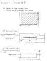
- Figure 7 illustrates a window pulse obtained by said timing pulse generator 1.
- a window signal such as shown in Figure 7(b) is derived.
- Figure 7(c) shows a horizontal partial enlargement of the signal. The sampling of the histogram is performed only when this window pulse takes a high-level.
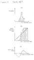
- FIG 8 graphically shows the operations of the luminance conversion performed by the conventional apparatus.
- a histogram wherein the input luminance levels are divided into suitable numbers as the one shown in Figure 8(a), is produced.
- the frequency distributions of the divided luminance levels are stored in the histogram memory 2 while the content of the memory is reset at a predetermined interval in order to reset the previously-stored data.
- This interval is generally set at an interval which equals a single vertical scanning period or an integer multiple.
- the lookup table arithmetical processing circuit 3 performs an accumulation of the histogram data, and it derives a normalizing coefficient which makes the accumulated maximum value equal to the maximum value of the output luminance level, and the processing circuit multiplies each data of the accumulative histogram to the derived normalizing coefficient. The results of this are stored in the lookup table 4.
- Figure 8(b) shows these operations.
- the content of the lookup table memory 4 is read out according to the luminance level of the input signal, and, as shown in Figure 8(c), the difference between the output and input luminance levels is outputted as a correction signal.
- the correction of the gradation is then performed by adding the correction signal to the input signal which is delayed by means of the delay circuit 5 using the adder 6.
- the distribution of the accumulative histogram stored in the lookup table contains a considerably high proportion of the low luminance components, as shown in Figure 9(d).
- the correction signal will take such a form shown in Figure 9(e).
- the correction is made to bring the luminance of the sub-display toward a higher level and, therefore, the luminance of the sub-display of which luminance level was originally high will be corrected toward a still higher level, bringing a definitely undesirable TV-viewing condition.
- the present invention relates to a gradation correcting apparatus capable of performing the optimum gradation correction dependent on the characteristics of the input signal, when the input video signal is a composite video signal consisting of main- and sub-display signals.
- the gradation of the sub-display can be corrected to an improved viewing condition by utilizing a main- and sub-display switching signal shown in Figure 9(c) which is outputted in synchronization with the sub-display signal.
- the gradation correcting apparatus of the present invention comprises:
- the signals of the main-display and the sub-display can be accurately separated by using said timing pulse generating means generating the window pulses and the first switching means using the window pulses and the main- and sub-display switching signals. Furthermore, based on the separated signals, a histogram of the luminance levels is produced in the histogram memory.
- the luminance information of the sub-display disposed within the main-display and the luminance information of the main-display excluding the sub-display are independently inputted to the correction signal outputting means, the arithmetical processing of the information including the mutual relationship between these two displays can be performed, and as the result of this, the correction signal can be produced.
- the correction signal is composited with the input video signal by means of the second switching means and the adding means.
- the gradation correction of the input video signal can be preformed according to the respective luminance level information of the main- and sub-displays.
- the gradation correction of the same can be performed at the precise timing by means of the delay means, an easy-to-see sub-display can be produced.
- the histogram memory stores the luminance levels of the input video signal representing either the sub-display domain or the predetermined domain excluding the sub-display domain according to the output of the first switching means in producing the histogram, the gradations of these two domains can be corrected independently, preventing possible interferences between these two domains.
- the correction signal output means is constituted of said lookup table arithmetical processing means which sequentially accumulates the frequencies of the luminance levels stored in the histogram memory and normalizes the maximum accumulated frequency so that it becomes equal to the maximum value of the output luminance signal, and the lookup table memory which memorizes the output of the lookup table arithmetical processing means, and simultaneously produces a correction signal from the difference between the output and the luminance level of the output luminance signal. Therefore, the correction signal precisely matched to the predetermined luminance level of the output luminance signal can be produced.
- the construction of the invented gradation correcting apparatus can be highly simplified by employing an interlocking switching circuit capable of switching the first and the second switching means simultaneously.
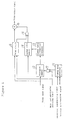
- Figure 1 is a block diagram of the gradation correcting apparatus showing a first exemplary embodiment of the invention.
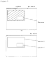
- Figure 2(a) shows a typical display screen produced by applying the first exemplary embodiment, and this shows also a pattern explaining a domain range from which the histograms are taken.
- Figure 2(b) shows a waveform explaining the operation at the horizontal rate obtained by applying the first exemplary embodiment of the invention.
- Figure 3(a) shows another example of the video signal display produced by applying the the first exemplary embodiment of the invention, and this also shows a pattern explaining a domain range from which the histograms are taken.
- Figure 3(b) is to show a pattern explaining the relationship between the main- and sub-displays.
- Figure 4 is a block diagram showing the construction of the gradation correcting appartus of the second exemplary embodiment of the invention.
- Figure 5(a) is a waveform showing an example of the main- and sub-display switching signal.
- Figure 5(b) shows histograms of the frequencies of the input luminance level and the normalized output luminance level of the main display. This shows also a correction signal outputted according to the historgrams.
- Figure 5(c) shows a histogram of the frequencies of the input luminance levels and the normalized output luminance levels of the sub-display and, at the same time, a correction signal outputted according to the histogram.
- Figure 6 is a block diagram showing the construction of a conventional gradation correcting apparatus. applying the conventional gradation correcting method.
- Figure 7(b) shows a waveform to explain the operation of the gradation correction at a vertical rate obtained by applying the conventional gradation correction method.
- Figure 7(c) shows a waveform to explain the operation at a horizontal rate obtained by applying the conventional gradation correction method.
- Figure 8(a) shows a histogram of the luminance levels of the input signal on the main-display.
- Figure 8(b) shows a histogram of the output luminance levels normalized for each input luminance level on the main-display.
- Figure 8(c) shows a graph of the correction signals outputted according to the histograms.
- Figure 9(a) shows a typical display pattern on the double display TV of the conventional construction.
- Figure 9(b) shows a waveform of video signal at the horizontal rate obtained by a conventional gradation correcting apparatus.
- Figure 9(c) shows a waveform of the main- and sub-display switching signal at the horizontal rate obtained by the conventional correcting apparatus.
- Figure 9(d) shows a histogram of the output luminance level which is normalized for every input luminance level on the double-display TV.
- Figure 9(e) shows a waveform of the correction signal outputted according to the histograms.
- Figure 1 is a block diagram showing the construction of the gradation correcting apparatus of the first exemplary embodiment.
- timing pulse generator 11 produces window pulses from both the horizontal and vertical synchronization signals, first AND circuit 17, as a first switching means, derives the AND between the window pulse and the main- and sub-display switching signal.
- Histogram memory 12 derives the histogram of gradation by storing the luminance levels of the input video signal according to the output of the first AND circuit 17, and lookup table arithmetical processing circuit 13 normalizes the maximum accumulated frequency in order to make this coincide with the maximum value of the output luminance signal.
- Lookup table memory 14 stores the normalized data and outputs the correction signals. Therefore, the correction signal output means is constituted of the lookup table arithmetical processing circuit 13 and the lookup table memory 14.
- Second AND circuit 18, as the second switching means derives the AND between the delayed main- and sub-display switching signal and the correction signal outputted at the lookup table memory 14.
- Adder 16, as the adding means adds the output of the second AND circuit 18 to the input signal delayed by the delay circuit 15.
- a window pulse is produced by the timing pulse generator 11, and an AND of the window pulse and the main- and sub-display switching signal is produced by the first AND circuit 17.
- the luminance levels of the input video signal are stored in the histogram memory 12 according to the output of the first AND circuit 17 in order to derive the histogram of the gradation.
- the histograms are then stored in the lookup table arithmetical processing circuit 13, and these values are normalized so that the maximum accumulated frequency becomes equal to the maximum value of the output luminance signal.
- the normalized data is stored in the lookup table memory 14, and the output of the memory 14 becomes available as the correction signal.
- the input signal and the main- and sub-display switching signal are delayed for a certain period in order to conduct the arithmetical processing by using the delay circuit 15.
- the correction signal at the sub-display domain is set at zero by deriving the AND of the correction signal and the delayed main- and sub-display switching signal by means of the second AND circuit 18.
- an appropriate correction according to the histogram of the main display can be given to the main display by adding the output of the second AND circuit 18 to the delayed input video signal by means of the adder 16, and the output signal maintaining the sub-display at its uncorrected state can be obtained.
- the sub-display held as it is, can be outputted because it is made independent of the gradation correction given to the main-display. This is obtained by combining the window pulse and the main- and sub-display switching signal. Therefore, as a result, the gradation correction makes the sub-display easier to view.
- the sub-display-B as it is can be obtained by setting the window pulse at a state to obtain a histogram of the surrounding domain of the sub-display-B, the gradation correction which makes the sub-display easier to see can be obtained as the result of this.
- Figure 4 is a block diagram showing the construction of a second exemplary gradation correcting apparatus.
- timing pulse generator 11 generates window pulses from the horizontal and vertical synchronization signals of the input video signal.
- Quintuple-ganged switch 19 switches the five memories simultaneously by means of the main- and sub-display switching signal.
- Histogram memory 12 stores the histograms of the luminance levels of main- and sub-displays independently.
- Lookup table arithmetical processing circuit 13 accumulatively stores the histograms and normalizes the maximum accumulated frequency so that the frequency thereof becomes equal to the maximum value of the output luminance signal.
- Lookup table memory 14 stores the normalized data for the main-display and the sub-display independently, and outputs the correction signal.
- Delay circuit 15 delays the input video signal. Although a correction by using a delay circuit is desirable, the boundaries generated by the gradation processing can be made less conspicuous by employing this practical and simple method shown in the embodiment of the invention.
- Adder 16 adds the correction signal to the delayed input video signal.
- the window pulse is generated by the timing pulse generator 11.
- the difference from the first exemplary embodiment is that five switches 19a to 19e incorporated within the quintuple-ganged switch 19 are simultaneously switched by the main- and sub-displays switching signal so that the histogram memory 12 and the lookup table memory 14 are switched to the main-display and the sub-display independently.
- the quintuple-ganged switch 19 consists of two switches 19a and 19c which switch two respective inputs to the histogram memories 12a and 12b, and the lookup table memories 14a and 14b, two switches 19b and 19e which switch two respective outputs from the histogram memories 12a and 12b, and the lookup table memories 14a and 14b, and the switch 19d which connects the output of the lookup table arithmetical processing circuit 13 to either of the two inputs of the lookup table memories 12a or 12b.
- the period of the sub-display is switched to use both the histogram memory 12a for the sub-display and the lookup table memory 14a by means for the main- and sub-display switching signal as shown in Figure 5(a).
- the period of the other is switched to use the histogram memory 12b for the main-display and the lookup table memory 14b.
- Figure 5(b) shows the operation which takes place during the period of the main-display.
- Figure 5(b) also shows a graph of the frequencies of the input luminance level histogram produced by the histopram memory 12b, plotted against the input luminance levels. The two frequencies are individually accumulated for each luminance level, and the graph of the frequencies is normalized so that the maximum accumulated frequency becomes equal to the maximum value of the output luminance signal.
- the normalized data is then stored in the lookup table memory 14b, and a correction signal becomes available as the output of the lookup table memory 14b.
- the five circuits are simultaneously switched by the quintuplely-ganged switch 19 during the period of sub-display and, by this, a correction signal becomes available from the lookup table memory 14a as shown in Figure 5(c).
- the correction signals dependent on the individual scenes of the main- and sub-displays can be derived and, by this, the gradation of the main- and sub-displays are corrected at their respective optimums.
- the gradation correction of the main-display and the gradation correction of the sub-display are independently performed according to the respective individual scenes. Therefore, both the main- and the sub-displays are corrected to show easy-to-see pictures.
- the luminance information of the sub-display disposed within a domain of the main-display and theiziminance information of the main-display excluding the domain of the sub-display is individually inputted into the gradation correction apparatus. Therefore, the relationship between these two displays can be derived arithmetically.
- the delay of the signal caused by the arithmetical processing is compensated by the delay means, and the gradations of the main- and sub-displays are properly corrected according to the respective luminance levels so that easy-to-see sub-displays are obtained on the respective displays.
- the histograms of the gradation of sub-display are excluded from the input signal by utilizing the main- and sub-display switching signal outputted in synchronizing with the sub-display.
- the histogram of gradation of sub-display and the histogram of gradation of main-display are independently processed by combining the input signal with the window pulse utilizing the main- and sub-display switching signal outputted in synchronizing with the sub-display.
- the gradation of the main-display is corrected according to the scene shown on the main-display, and the gradation of the sub-display is corrected according to the scene shown in the sub-display, so that the gradation correction apparatus realizing easy-to-see gradations of both the main- and sub-displays is realized.
Landscapes
- Engineering & Computer Science (AREA)
- Multimedia (AREA)
- Signal Processing (AREA)
- Picture Signal Circuits (AREA)
- Transforming Electric Information Into Light Information (AREA)
- Control Of Indicators Other Than Cathode Ray Tubes (AREA)
Applications Claiming Priority (2)
| Application Number | Priority Date | Filing Date | Title |
|---|---|---|---|
| JP115697/92 | 1992-05-08 | ||
| JP4115697A JPH05316446A (ja) | 1992-05-08 | 1992-05-08 | 階調補正装置 |
Publications (2)
| Publication Number | Publication Date |
|---|---|
| EP0569018A1 true EP0569018A1 (de) | 1993-11-10 |
| EP0569018B1 EP0569018B1 (de) | 1998-08-05 |
Family
ID=14668999
Family Applications (1)
| Application Number | Title | Priority Date | Filing Date |
|---|---|---|---|
| EP93107376A Expired - Lifetime EP0569018B1 (de) | 1992-05-08 | 1993-05-06 | Gradationskorrekturvorrichtung |
Country Status (4)
| Country | Link |
|---|---|
| US (1) | US5359369A (de) |
| EP (1) | EP0569018B1 (de) |
| JP (1) | JPH05316446A (de) |
| DE (1) | DE69320093T2 (de) |
Cited By (6)
| Publication number | Priority date | Publication date | Assignee | Title |
|---|---|---|---|---|
| US5544761A (en) * | 1994-10-24 | 1996-08-13 | Zdroik; Jerome J. | Soft cranberry and undersize cranberry separator and method |
| WO1998048571A1 (en) * | 1997-04-23 | 1998-10-29 | Thomson Consumer Electronics, Inc. | Control of video level by region and content of information displayed |
| EP0877527A3 (de) * | 1997-05-06 | 2001-11-28 | Matsushita Electric Industrial Co., Ltd. | Vorrichtung zur Verarbeitung eines Videosignals |
| EP1164784A1 (de) * | 2000-06-13 | 2001-12-19 | Koninklijke Philips Electronics N.V. | Verhinderung des Wölbungsphänomens |
| US6809776B1 (en) | 1997-04-23 | 2004-10-26 | Thomson Licensing S.A. | Control of video level by region and content of information displayed |
| KR101466596B1 (ko) * | 2006-11-27 | 2014-11-28 | 돌비 레버러토리즈 라이쎈싱 코오포레이션 | 디지털 이미지들에서의 동적 범위를 부스팅하기 위한 장치 및 방법들 |
Families Citing this family (17)
| Publication number | Priority date | Publication date | Assignee | Title |
|---|---|---|---|---|
| CN1135140A (zh) * | 1995-02-27 | 1996-11-06 | 松下电器产业株式会社 | 用于多重图像显示的补偿电压发生装置及其视频显示装置 |
| JP3755921B2 (ja) * | 1996-02-29 | 2006-03-15 | 株式会社コダックデジタルプロダクトセンター | 撮像デバイスのラインノイズ除去方法及びそれを用いたラインノイズ除去装置 |
| US5936684A (en) * | 1996-10-29 | 1999-08-10 | Seiko Epson Corporation | Image processing method and image processing apparatus |
| JP4155723B2 (ja) * | 2001-04-16 | 2008-09-24 | 富士フイルム株式会社 | 画像管理システム及び画像管理方法、並びに画像表示装置 |
| JP2004032551A (ja) * | 2002-06-27 | 2004-01-29 | Seiko Epson Corp | 画像処理方法、画像処理装置及びプロジェクタ |
| TWI289291B (en) * | 2003-04-29 | 2007-11-01 | Sunplus Technology Co Ltd | Sub-screen image decoder |
| US20050172182A1 (en) * | 2004-01-15 | 2005-08-04 | Elias Gedamu | Optimal operational voltage identification for a processor design |
| JP4078649B2 (ja) * | 2004-01-28 | 2008-04-23 | 日本ビクター株式会社 | 映像信号処理装置及び方法 |
| US8285041B2 (en) * | 2004-09-14 | 2012-10-09 | Olympus Corporation | Image processing apparatus, image recording apparatus, and image processing method |
| JP2007067571A (ja) * | 2005-08-29 | 2007-03-15 | Fujitsu Ltd | 画像処理装置 |
| US7474415B2 (en) * | 2006-09-13 | 2009-01-06 | Chung Shan Institute Of Science And Technology, Armaments Bureau, M.N.D. | Measurement method of three-dimensional profiles and reconstruction system thereof using subpixel localization with color gratings and picture-in-picture switching on single display |
| JP2009055231A (ja) * | 2007-08-24 | 2009-03-12 | Sharp Corp | 動画表示処理装置、動画データ多重化装置、動画表示方法、コンピュータプログラム及び記録媒体 |
| US20090135449A1 (en) * | 2007-11-27 | 2009-05-28 | Kabushiki Kaisha Toshiba | Image forming apparatus |
| JP5072742B2 (ja) * | 2008-07-02 | 2012-11-14 | シャープ株式会社 | 画像処理装置及び画像処理方法 |
| JP5561524B2 (ja) * | 2010-03-19 | 2014-07-30 | ソニー株式会社 | 画像処理装置および方法、並びにプログラム |
| JP5637383B2 (ja) * | 2010-12-15 | 2014-12-10 | ソニー株式会社 | 画像処理装置、画像処理方法、およびプログラム |
| JP2013041400A (ja) * | 2011-08-15 | 2013-02-28 | Sony Corp | 画像処理装置、画像処理方法、およびプログラム |
Citations (2)
| Publication number | Priority date | Publication date | Assignee | Title |
|---|---|---|---|---|
| EP0258740A2 (de) * | 1986-09-02 | 1988-03-09 | Fuji Photo Film Co., Ltd. | Verfahren und Vorrichtung zur Bildverarbeitung mit Gradationskorrektur des Bildsignals |
| EP0393946A2 (de) * | 1989-04-18 | 1990-10-24 | Thomson Consumer Electronics, Inc. | Videosignalsteuerschaltung |
Family Cites Families (8)
| Publication number | Priority date | Publication date | Assignee | Title |
|---|---|---|---|---|
| JPS5676691A (en) * | 1979-11-28 | 1981-06-24 | Hitachi Ltd | Television receiver with plurality of screen display |
| US4578698A (en) * | 1982-06-18 | 1986-03-25 | Matsushita Electric Industrial Co., Ltd. | Multiple display control apparatus for a television receiver |
| FI842333A7 (fi) * | 1984-06-08 | 1985-12-09 | Valtion Teknillinen Tutkimuskeskus | Foerfarande foer identifiering av de mest foeraendrade bildomraodena i levande videosignal. |
| JPH03235585A (ja) * | 1990-02-13 | 1991-10-21 | Sharp Corp | 2画面表示装置 |
| JPH03263984A (ja) * | 1990-03-14 | 1991-11-25 | Matsushita Electric Ind Co Ltd | 映像処理装置 |
| JP2680731B2 (ja) * | 1990-09-18 | 1997-11-19 | 三洋電機株式会社 | 2画面テレビジョン受像機 |
| JPH04271669A (ja) * | 1991-02-27 | 1992-09-28 | Matsushita Electric Ind Co Ltd | 階調補正装置 |
| JPH0799862B2 (ja) * | 1991-03-22 | 1995-10-25 | 松下電器産業株式会社 | 階調補正装置 |
-
1992
- 1992-05-08 JP JP4115697A patent/JPH05316446A/ja active Pending
-
1993
- 1993-05-06 DE DE69320093T patent/DE69320093T2/de not_active Expired - Fee Related
- 1993-05-06 EP EP93107376A patent/EP0569018B1/de not_active Expired - Lifetime
- 1993-05-10 US US08/059,910 patent/US5359369A/en not_active Expired - Lifetime
Patent Citations (2)
| Publication number | Priority date | Publication date | Assignee | Title |
|---|---|---|---|---|
| EP0258740A2 (de) * | 1986-09-02 | 1988-03-09 | Fuji Photo Film Co., Ltd. | Verfahren und Vorrichtung zur Bildverarbeitung mit Gradationskorrektur des Bildsignals |
| EP0393946A2 (de) * | 1989-04-18 | 1990-10-24 | Thomson Consumer Electronics, Inc. | Videosignalsteuerschaltung |
Cited By (10)
| Publication number | Priority date | Publication date | Assignee | Title |
|---|---|---|---|---|
| US5544761A (en) * | 1994-10-24 | 1996-08-13 | Zdroik; Jerome J. | Soft cranberry and undersize cranberry separator and method |
| WO1998048571A1 (en) * | 1997-04-23 | 1998-10-29 | Thomson Consumer Electronics, Inc. | Control of video level by region and content of information displayed |
| US6809776B1 (en) | 1997-04-23 | 2004-10-26 | Thomson Licensing S.A. | Control of video level by region and content of information displayed |
| KR100526740B1 (ko) * | 1997-04-23 | 2005-11-08 | 톰슨 콘슈머 일렉트로닉스, 인코포레이티드 | 디스플레이될 정보의 영역 및 내용물에 의한 비디오 레벨 제어 시스템 및 방법 |
| EP0877527A3 (de) * | 1997-05-06 | 2001-11-28 | Matsushita Electric Industrial Co., Ltd. | Vorrichtung zur Verarbeitung eines Videosignals |
| EP1164784A1 (de) * | 2000-06-13 | 2001-12-19 | Koninklijke Philips Electronics N.V. | Verhinderung des Wölbungsphänomens |
| WO2001097508A1 (en) * | 2000-06-13 | 2001-12-20 | Koninklijke Philips Electronics N.V. | Preventing doming phenomena |
| US6741295B2 (en) | 2000-06-13 | 2004-05-25 | Koninklijke Philips Electronics N.V. | Preventing doming phenomena |
| KR101466596B1 (ko) * | 2006-11-27 | 2014-11-28 | 돌비 레버러토리즈 라이쎈싱 코오포레이션 | 디지털 이미지들에서의 동적 범위를 부스팅하기 위한 장치 및 방법들 |
| NO338509B1 (no) * | 2006-11-27 | 2016-08-29 | Dolby Laboratories Licensing Corp | Anordning og metode for å bedre dynamisk område i digitale bilder |
Also Published As
| Publication number | Publication date |
|---|---|
| US5359369A (en) | 1994-10-25 |
| DE69320093T2 (de) | 1998-12-10 |
| JPH05316446A (ja) | 1993-11-26 |
| EP0569018B1 (de) | 1998-08-05 |
| DE69320093D1 (de) | 1998-09-10 |
Similar Documents
| Publication | Publication Date | Title |
|---|---|---|
| EP0569018B1 (de) | Gradationskorrekturvorrichtung | |
| EP0651577B1 (de) | Digitales Fernsehsystem | |
| US5793433A (en) | Apparatus and method for vertically extending an image in a television system | |
| US4524379A (en) | Double-scanning non-interlace television receiver with vertical aperture correction circuit | |
| US5459477A (en) | Display control device | |
| US5534934A (en) | Television receiver capable of enlarging and compressing image | |
| US5159438A (en) | Aspect ratio conversion of television display | |
| JPS63198485A (ja) | キー信号発生器 | |
| US20080043145A1 (en) | Image Processing Apparatus, Image Processing Method, and Image Display Apparatus | |
| US5301025A (en) | Parabolic waveform generating apparatus | |
| US5390028A (en) | Apparatus for converting input video signal to motion picture film image | |
| US4899220A (en) | Method and apparatus for recombining a main panel component with a augmentation panel component to create a wide aspect ratio televison display | |
| EP0480910A2 (de) | Bildanzeigesystem | |
| JPH0652943B2 (ja) | 映像機器 | |
| EP0658046B1 (de) | Videosignalverarbeitungsgerät und -verfahren | |
| US5241390A (en) | Digital soft wipe signal generating apparatus | |
| EP0659015A1 (de) | Bildsynchronisierer und Signalumschaltgerät | |
| US4847679A (en) | Multiplex chrominance gain control and matrix using a single multiplier and a coefficient shift register | |
| JPH02213283A (ja) | 輪郭強調量調整回路およびテレビジョン受像機 | |
| JPS63316594A (ja) | 送受信システム及び装置 | |
| JPH0130350B2 (de) | ||
| JPH0683419B2 (ja) | テレビジョン信号受信装置 | |
| JPH06125482A (ja) | 黒レベル補正回路の補正範囲指定回路 | |
| KR100228728B1 (ko) | 영상기기의 윤곽보정회로 | |
| JPS63316583A (ja) | 2チャネル広アスペクト比テレビジョン信号伝送システムの1チェネル上で拡大パネル成分を伝送する方法と装置 |
Legal Events
| Date | Code | Title | Description |
|---|---|---|---|
| PUAI | Public reference made under article 153(3) epc to a published international application that has entered the european phase |
Free format text: ORIGINAL CODE: 0009012 |
|
| AK | Designated contracting states |
Kind code of ref document: A1 Designated state(s): DE FR GB IT |
|
| 17P | Request for examination filed |
Effective date: 19931227 |
|
| 17Q | First examination report despatched |
Effective date: 19960202 |
|
| GRAG | Despatch of communication of intention to grant |
Free format text: ORIGINAL CODE: EPIDOS AGRA |
|
| GRAG | Despatch of communication of intention to grant |
Free format text: ORIGINAL CODE: EPIDOS AGRA |
|
| GRAG | Despatch of communication of intention to grant |
Free format text: ORIGINAL CODE: EPIDOS AGRA |
|
| GRAH | Despatch of communication of intention to grant a patent |
Free format text: ORIGINAL CODE: EPIDOS IGRA |
|
| GRAH | Despatch of communication of intention to grant a patent |
Free format text: ORIGINAL CODE: EPIDOS IGRA |
|
| GRAA | (expected) grant |
Free format text: ORIGINAL CODE: 0009210 |
|
| AK | Designated contracting states |
Kind code of ref document: B1 Designated state(s): DE FR GB IT |
|
| REF | Corresponds to: |
Ref document number: 69320093 Country of ref document: DE Date of ref document: 19980910 |
|
| ET | Fr: translation filed | ||
| PLBE | No opposition filed within time limit |
Free format text: ORIGINAL CODE: 0009261 |
|
| 26N | No opposition filed | ||
| PGFP | Annual fee paid to national office [announced via postgrant information from national office to epo] |
Ref country code: DE Payment date: 20010430 Year of fee payment: 9 |
|
| PGFP | Annual fee paid to national office [announced via postgrant information from national office to epo] |
Ref country code: GB Payment date: 20010502 Year of fee payment: 9 |
|
| PGFP | Annual fee paid to national office [announced via postgrant information from national office to epo] |
Ref country code: FR Payment date: 20010518 Year of fee payment: 9 |
|
| REG | Reference to a national code |
Ref country code: GB Ref legal event code: IF02 |
|
| PG25 | Lapsed in a contracting state [announced via postgrant information from national office to epo] |
Ref country code: GB Free format text: LAPSE BECAUSE OF NON-PAYMENT OF DUE FEES Effective date: 20020506 |
|
| PG25 | Lapsed in a contracting state [announced via postgrant information from national office to epo] |
Ref country code: DE Free format text: LAPSE BECAUSE OF NON-PAYMENT OF DUE FEES Effective date: 20021203 |
|
| GBPC | Gb: european patent ceased through non-payment of renewal fee |
Effective date: 20020506 |
|
| PG25 | Lapsed in a contracting state [announced via postgrant information from national office to epo] |
Ref country code: FR Free format text: LAPSE BECAUSE OF NON-PAYMENT OF DUE FEES Effective date: 20030131 |
|
| REG | Reference to a national code |
Ref country code: FR Ref legal event code: ST |
|
| PG25 | Lapsed in a contracting state [announced via postgrant information from national office to epo] |
Ref country code: IT Free format text: LAPSE BECAUSE OF NON-PAYMENT OF DUE FEES Effective date: 20050506 |