EP0570143A2 - Procédé et dispositif d'interface de signal de données sériel - Google Patents
Procédé et dispositif d'interface de signal de données sériel Download PDFInfo
- Publication number
- EP0570143A2 EP0570143A2 EP93303458A EP93303458A EP0570143A2 EP 0570143 A2 EP0570143 A2 EP 0570143A2 EP 93303458 A EP93303458 A EP 93303458A EP 93303458 A EP93303458 A EP 93303458A EP 0570143 A2 EP0570143 A2 EP 0570143A2
- Authority
- EP
- European Patent Office
- Prior art keywords
- data
- clock signal
- signal
- sampling
- instant
- Prior art date
- Legal status (The legal status is an assumption and is not a legal conclusion. Google has not performed a legal analysis and makes no representation as to the accuracy of the status listed.)
- Granted
Links
- 238000000034 method Methods 0.000 title claims abstract description 23
- 238000005070 sampling Methods 0.000 claims description 30
- 230000001419 dependent effect Effects 0.000 claims description 2
- IYZMXHQDXZKNCY-UHFFFAOYSA-N 1-n,1-n-diphenyl-4-n,4-n-bis[4-(n-phenylanilino)phenyl]benzene-1,4-diamine Chemical compound C1=CC=CC=C1N(C=1C=CC(=CC=1)N(C=1C=CC(=CC=1)N(C=1C=CC=CC=1)C=1C=CC=CC=1)C=1C=CC(=CC=1)N(C=1C=CC=CC=1)C=1C=CC=CC=1)C1=CC=CC=C1 IYZMXHQDXZKNCY-UHFFFAOYSA-N 0.000 abstract description 3
- 239000000872 buffer Substances 0.000 description 4
- 238000012545 processing Methods 0.000 description 4
- 238000013459 approach Methods 0.000 description 3
- 230000001934 delay Effects 0.000 description 2
- 238000010586 diagram Methods 0.000 description 2
- 238000007429 general method Methods 0.000 description 2
- 230000000630 rising effect Effects 0.000 description 2
- 230000007704 transition Effects 0.000 description 2
- 230000003111 delayed effect Effects 0.000 description 1
- 238000012986 modification Methods 0.000 description 1
- 230000004048 modification Effects 0.000 description 1
- 238000000926 separation method Methods 0.000 description 1
- 238000010998 test method Methods 0.000 description 1
- 238000012360 testing method Methods 0.000 description 1
- 238000012956 testing procedure Methods 0.000 description 1
Images



Classifications
-
- G—PHYSICS
- G11—INFORMATION STORAGE
- G11C—STATIC STORES
- G11C7/00—Arrangements for writing information into, or reading information out from, a digital store
- G11C7/22—Read-write [R-W] timing or clocking circuits; Read-write [R-W] control signal generators or management
- G11C7/222—Clock generating, synchronizing or distributing circuits within memory device
-
- H—ELECTRICITY
- H04—ELECTRIC COMMUNICATION TECHNIQUE
- H04L—TRANSMISSION OF DIGITAL INFORMATION, e.g. TELEGRAPHIC COMMUNICATION
- H04L7/00—Arrangements for synchronising receiver with transmitter
- H04L7/0008—Synchronisation information channels, e.g. clock distribution lines
- H04L7/0012—Synchronisation information channels, e.g. clock distribution lines by comparing receiver clock with transmitter clock
-
- G—PHYSICS
- G11—INFORMATION STORAGE
- G11C—STATIC STORES
- G11C19/00—Digital stores in which the information is moved stepwise, e.g. shift registers
- G11C19/28—Digital stores in which the information is moved stepwise, e.g. shift registers using semiconductor elements
-
- H—ELECTRICITY
- H04—ELECTRIC COMMUNICATION TECHNIQUE
- H04N—PICTORIAL COMMUNICATION, e.g. TELEVISION
- H04N7/00—Television systems
- H04N7/025—Systems for the transmission of digital non-picture data, e.g. of text during the active part of a television frame
- H04N7/035—Circuits for the digital non-picture data signal, e.g. for slicing of the data signal, for regeneration of the data-clock signal, for error detection or correction of the data signal
Definitions
- the present invention relates to interfacing a data signal and an associated external clock signal to a circuit.
- One approach to the problem of feeding a data signal and its associated external clock signal to a circuit is to use the external clock signal to determine when to read in each bit of the data signal, and, if the circuit processes the data signal further using clocked logic, also to use that external clock to drive that clocked logic.
- the circuit required is relatively complex, the buffer needs to be capable of being operated by two different clocks while the rest of the circuit remains connected always to only one or other of the clocks. Also having two clocks makes the usual method of testing a circuit by clocking through test patterns difficult to apply.
- a method of reading a data signal including providing a local clock signal having a higher freqency than the data clock signal, sampling the data clock signal at time instants referenced to the local clock signal, determining from the data clock samples particular time instants referenced to the local clock signal, and reading the data signal at the particular time instants, so that each bit of the data signal is read once and only once during that portion of the bit period that the value of the bit is stable.
- the particular time instants determined from the data clock samples are whole numbers of periods of the local clock signal after the time instants when the data clock signal was sampled, the number of periods depending on the value of the sample of the data clock signal obtained.
- the data clock signal may consist of marks and spaces of substantially equal duration and the number of periods may be one if the sampled value of the data clock signal is a mark and two if the sampled value of the data clock signal is a space.
- apparatus for reading a data signal having an associated data clock signal with a frequency equal to the bit rate of the data signal including clock means for producing a local clock signal having a higher frequency than the data clock signal, first and second latches clocked by the local clock signal, the first latch being connected to receive the data clock signal as a digit input and producing an output bit applied as a digit input to the second latch, gating means responsive to the output bits of the latches and the local clock signal to produce as output selected parts of the local clock signal having an average frequency equal to the bit rate of the data signal, and means responsive to the output of the gating means to sample each bit of the data signal while it has a stable value.
- the general approach of the present invention is not to provide complex buffers which can be controlled by both the local clock and the data clock but rather to sample the data clock to ascertain sufficient information as to the location of the bits within the data signal and then to read the data signal, both the sampling of the data clock signal and the reading of the data signal being under the control of the local clock.
- This of course can be achieved by sampling the data clock signal many times during each of its periods and comparing these samples with each other to ascertain the location of features of the clock signal such as positive and negative going edges and hence the location of the bits within the data signal.
- the present invention is designed to deal with such circumstances where it is desirable to interface a data signal and an associated data clock signal to a circuit operating at a slightly faster clock rate, although it can be used where other circumstances obtain.
- a clock signal TCLK derived from a received teletext signal is applied via an input terminal 1 and through an inverter 2 to the clock input of a D-type flip-flop 3 and to the digit input of a D-type flip-flop 4.
- a data signal TDATA derived from the received teletext signal is applied via a second input terminal 5 to the digit input of the flip-flop 3.
- Locally generated two-phase clock signals LCLK1 and LCLK2 are applied via input terminals 6 and 6' to respective clock inputs of the flip-flop 4 and of another D-type flip-flop 7.
- the flip-flops 4 and 7 are of the master-slave type having two separate clock inputs.
- the clock signal LCLK1 is also connected to an input of a 2-input AND gate 8.
- the Q output of the flip-flop 4 is connected to the digit input of the flip-flop 7 and also to an input of a 2-input NAND gate 9.
- the second input of the NAND gate 9 is connected to receive the Q ⁇ output of the flip-flop 7.
- the output of the NAND gate 9 is connected to the second input of the AND gate 8.
- the output of the AND gate 8 is a modified LCLK1 clock signal and together with the unmodified LCLK2 clock signal is applied to the respective clock inputs of two D-type flip-flops 10 and 11 , also of the master-slave type, forming the first two stages of a shift register used to convert the teletext data from serial to parallel format.
- the modified LCLK1 clock signal and the clock signal LCLK2 are also applied to the clock inputs of the remaining stages of that shift register formed by flip-flops of the same type as 10 and 11 (not shown) and via terminals 12 and 12' to other parts of the system (also not shown) such as bit and character counters controlling the forwarding of the received data.
- the Q output of the flip-flop 3 at which stable data SDATA appears is connected to the digit input of the flip-flop 10.
- the Q output of the flip-flop 10 is connected to the digit input of the flip-flop 11, similar connections being made between the flip-flops forming the other stages of the shift register.
- the flip-flops 4 and 7 sample the signals applied to their digit inputs at the negative going edges of the local clock signal LCLK1, the flip flops of the shift register 10, 11 sample the signals applied to their digit inputs at the negative going edges of the modified clock signal and the flip flop 3 samples the signal applied to its digit input at the negative going edges of TCLK which are, of course, the same times as the positive going edges of the inverted TCLK signal applied to the clock input of flip flop 4.
- the data of a teletext signal is in binary form using non-return-to-zero (NRZ) coding at a bit rate of 6.9375 MHz.
- the teletext data is separated from the television signal on which it was carried, and a clock signal is derived from the data and is used to stabilise the timing of the data using the flip-flop 3.
- the stabilised data bits appear sequentially at the Q output of the flip-flop 3.
- a locally generated clock having a frequency of either 11.0 MHz or 11.5625 MHz depending on whether a voltage controlled oscillator or a frequency multiplier is used to generate signals for the display of the teletext data.
- a purpose of the circuit shown in Figure 1 is to receive the teletext data at its bit rate of 6.9375 MHz and to enable it to be processed by circuitry working under the control of a clock running at 11.0 MHz or 11.5625 MHz.
- the AND gate 8 is opened to allow selected ones of the pulses of the first phase LCLK1 of the locally generated clock to pass so as to produce a modified clock signal having an average frequency of 6.9375 MHz.
- Such a modified clock signal will clock the bits of the teletext data into the shift register at the rate of the modified clock signal despite the fact that the second phase LCLK2 is not modified.
- the modified clock signal therefore enables the bits of the teletext data to be sent on for processing in their correct groups.
- the circuitry of Figure 1 executes the following algorithm: IF (PRESENT SAMPLED TCLK IS HIGH) [CONDITION 1] OR IF (PREVIOUS SAMPLED TCLK IS LOW) [CONDITION 2] THEN READ SDATA ON THE NEXT ACTIVE TRANSITION OF LCLK1
- the TCLK samples are stored in inverse form in the flip-flops 4 and 7, the flip-flop 4 storing the inverse of the present TCLK sample and flip-flop 7 storing the inverse of the previous TCLK sample.
- the NAND gate 9 responds to the Q output of the flip-flop 4 and the Q ⁇ output of the flip-flop 7 so as to produce a HIGH output if either (or both) of the Q output of flip-flop 4 and the Q ⁇ output of flip-flop 7 is low. Taking into account the inversion by the inverter 2, it follows that the output of the gate 9 is HIGH if CONDITION 1 or CONDITION 2 is met.
- the output of the gate 9 controls the gate 8 so as to pass the pulses of LCLK1 to the shift register stages 10, 11 and the terminal 12 in accordance with the algorithm.
- the general method of the algorithm is to sample TCLK one or more times during a bit of SDATA, to recognise whether each sample corresponds to a HIGH or LOW portion of TCLK and then to chose for each TCLK sample a time relative to the sampling instant at which to read SDATA, that time being during the next bit of SDATA after the instant at which the corresponding sample of TCLK was taken.
- any algorithm in accordance with the above general method should also provide a method of ensuring that, where more than one choice of time is available for a particular bit of SDATA, SDATA is actually read once only.
- the particular algorithm that the circuit of Figure 1 employs ensures that, by sampling TCLK and reading SDATA only at discrete times under the control of the local clock LCLK1, and by ensuring that, if more than one sample of TCLK is available during a bit of SDATA so that a plurality of choices of times to read SDATA during the next bit are available, then the choices are all for the same time, thus resulting in that bit of SDATA being read only once.
- FIG. 2 is a diagram illustrating the operation of the algorithm.
- TTC and TLC stand for the period times of the teletext clock and the local clock respectively.
- Bar A represents times at which TCLK is HIGH and would be sampled as HIGH. As can be seen from the statement of the algorithm such a sample results in SDATA being read one period of LCLK1 later.
- SDATA the output flip-flop 3
- flip-flop 10 the output flip-flop 3
- bar B one period of LCLK1 later than bar A which therefore represents the times at which the resulting read operation would take place.
- Bar C represents times at which TCLK is LOW and would be sampled at LOW.
- Bar D represents the times at which the corresponding read would occur two periods of LCLK1 later.
- gate 8 passes to the flip-flop 10 only the pulses of LCLK1 selected by the algorithm; in practice gate 8 can be open for a period corresponding to the start of the bar B until the end of bar D.
- X and Y represent periods at the beginning and end of a bit during which SDATA may be changing therefore making the reading of SDATA unreliable. Where these periods are significant the above restrictions, if SDATA is to be read during its stable period, need to be modified to TLC > TC2 + X TLC ⁇ TTC - Y 2 x TLC > TTC + X 2 x TLC ⁇ TC2 + TTC - Y.
- the algorithm ensures that where more than one choice of time is available for reading a particular bit of SDATA that bit is in fact read only once.
- the maximum number of samples of TCLK during one bit is two, once during the low period of TCLK (Bar C) and once during its high period (Bar A). Since the sample of TCLK during Bar A would be TTC later than that during bar C and the respective choices of the times to read SDATA are one and two times TTC then those choices will be for exactly the same time.
- SDATA is read only once during that bit; in Figure 2 the read point would be during the overlap of Bar B and Bar D.
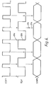
- Figures 3 and 4 illustrate the ability of the algorithm to enable a bit of SDATA to be read correctly despite incorrect sampling of TCLK (in the circuit of Figure 1 the inverted form of TCLK is sampled by flip-flop 4).
- Figures 3 and 4 show the waveforms of those signals, LCLK1 the local clock, TCLK the teletext clock and SDATA the stabilised teletext data. Arrows represent sample times.
- the negative going edges of LCLK1 determine the times at which TCLK is sampled. Those are represented by the arrows 12, 13, 14a, 14b, 15 and 16. The arrows also indicate the value of TCLK at the times of sampling, short arrows representing HIGH and long arrows representing LOW.
- the times, determined by the algorithm, when SDATA is sampled are represented by the arrows 17, 18a, 18b and 19.
- sample 14 of TCLK it can be seen that it is very close to a positive going edge of TCLK with the result that the sample taken may be HIGH 14a or LOW 14b. However, that uncertainty does not affect the value of SDATA sampled.
- SDATA is sampled at 18a, and similarly for LOW 14b SDATA is sampled at 18b, which is within the same bit of SDATA. That means that whatever value is obtained when TCLK is sampled at 14 the same value is obtained for the resulting sample of SDATA.
- Figure 5 illustrates some other restrictions on the ratio between the periods of TCLK and LCLK1 which are a consequence of possible incorrect sampling of TCLK illustrated in figures 3 and 4.
- the algorithm employed by the circuit of Figure 1 to enable a bit of SDATA to be read correctly despite an incorrect sampling of TCLK it is a requirement that if a sampling of TCLK could provide an uncertain value then the immediately preceding and the immediately following samples should provide definite values.
- the waveform TCLK is shown and also a waveform showing the values which TCLK would provide when sampled but only for those parts of TCLK for which the sample value is certain; the blank intervals on each side of the falling and rising edges of TCLK, where the sampling of TCLK would provide uncertain values, are marked DF1, DF2, DR1, DR2 respectively.
- Arrows 22 and 23 represent two samples of TCLK taken TLC apart; if their separation were reduced it would be possible for two consecutive uncertain samples to occur, for example sample 22 during the interval DF and sample 23 during the interval DR.
- the resulting restriction on the ratio between the period of TCLK and LCLK is TLC > TC1 + DF1 + DR2.
- Arrows 24 and 25 represent two similar samples to 22 and 23 but where the first is close to a rising rather than a falling edge of TCLK.
- the corresponding restriction is: TLC > TC2 + DR1 + DF2
- the two restrictions can be combined to give: 2 x TLC > TTC + DR + DF which unlike those discussed in relation to figure 2, is independent of the mark to space ratio of TCLK, unless of course the intervals DR and DF were to overlap.
- the period of the local clock TLC can be between 0.5 and 1.0 times that of the data clock TTC if DR and DF are negligible.
- the mark to space ratio dependent restrictions limit this further, of course, depending on the particular mark to space ratio of the data clock TCLK.
- a mark to space ratio of 1:1 has in general some advantages, for example absence of a DC level if mark and space are represented by equal and opposite voltages.
- TLC is limited to being between 0.5 and 0.75 times TTC.
- the frequencies involved are 6.9375 MHz for TCLK and TDATA and either 11.0 MHz or 11.5625 MHz for LCLK1 and LCLK2 which satisfy the above limitations.
- the invention can, of couse, be applied to other types of signals and to other clock frequencies within the limitations indicated.
- the flip-flops 4, 7, 10 and 11 may be of a type, such as TDN11, which in addition to being of the two phase type have a second digit input and a third clock input which can be employed to connect the flip-flops into a long shift register so that the circuit, including those parts not shown or described, can be put through a scan-testing procedure.
- the description of Figure 1 above refers to the locally generated clock signal LCLK1 having an associated second clock signal LCLK2 in antiphase with it. It would of course be possible to have the flip flops 4, 7, 10, 11 as single phase ones operated by LCLK1 or the modified clock signal alone if those signals are appropriately delayed before being applied to each of those flip flops.
Landscapes
- Engineering & Computer Science (AREA)
- Signal Processing (AREA)
- Computer Networks & Wireless Communication (AREA)
- Multimedia (AREA)
- Synchronisation In Digital Transmission Systems (AREA)
- Dc Digital Transmission (AREA)
- Information Transfer Systems (AREA)
Applications Claiming Priority (2)
| Application Number | Priority Date | Filing Date | Title |
|---|---|---|---|
| GB9210414 | 1992-05-15 | ||
| GB929210414A GB9210414D0 (en) | 1992-05-15 | 1992-05-15 | Method and apparatus for interfacing a serial data signal |
Publications (3)
| Publication Number | Publication Date |
|---|---|
| EP0570143A2 true EP0570143A2 (fr) | 1993-11-18 |
| EP0570143A3 EP0570143A3 (fr) | 1994-10-12 |
| EP0570143B1 EP0570143B1 (fr) | 1999-12-08 |
Family
ID=10715534
Family Applications (1)
| Application Number | Title | Priority Date | Filing Date |
|---|---|---|---|
| EP93303458A Expired - Lifetime EP0570143B1 (fr) | 1992-05-15 | 1993-05-04 | Procédé et dispositif d'interface de signal de données sériel |
Country Status (6)
| Country | Link |
|---|---|
| US (1) | US6115548A (fr) |
| EP (1) | EP0570143B1 (fr) |
| JP (1) | JPH0653951A (fr) |
| KR (1) | KR100310948B1 (fr) |
| DE (1) | DE69327193T2 (fr) |
| GB (1) | GB9210414D0 (fr) |
Cited By (1)
| Publication number | Priority date | Publication date | Assignee | Title |
|---|---|---|---|---|
| WO1999023787A3 (fr) * | 1997-11-03 | 1999-07-15 | Analog Devices Inc | Point d'acces pour communication bidirectionnelle d'une unite de traitement de signaux numeriques |
Families Citing this family (1)
| Publication number | Priority date | Publication date | Assignee | Title |
|---|---|---|---|---|
| DE69801827T2 (de) * | 1998-11-14 | 2002-03-28 | Agilent Technologies, Inc. (N.D.Ges.D.Staates Delaware) | Taktgenerator |
Family Cites Families (11)
| Publication number | Priority date | Publication date | Assignee | Title |
|---|---|---|---|---|
| FR497012A (fr) * | 1919-11-12 | 1919-11-22 | Daniel Avisse | Timbre-composteur à rubans |
| FR37299E (fr) * | 1929-08-02 | 1930-11-03 | Phare pour véhicules | |
| US3980993A (en) * | 1974-10-17 | 1976-09-14 | Burroughs Corporation | High-speed/low-speed interface for data processing systems |
| FR2459585A1 (fr) * | 1979-06-20 | 1981-01-09 | Thomson Csf | Procede et dispositif pour l'affinage de la remise en phase d'une horloge locale |
| FR2479620B1 (fr) * | 1980-03-28 | 1988-01-08 | Thomson Csf | Dispositif de synchronisation d'informations numeriques transmises par paquets et recepteur comportant un tel dispositif |
| US4673979A (en) * | 1984-06-15 | 1987-06-16 | Matsushita Electric Industrial Co., Ltd. | Digital data reproducing system |
| JP2588195B2 (ja) * | 1987-05-28 | 1997-03-05 | 株式会社東芝 | パルス入力装置 |
| US5040109A (en) * | 1988-07-20 | 1991-08-13 | Digital Equipment Corporation | Efficient protocol for communicating between asychronous devices |
| US4949361A (en) * | 1989-06-26 | 1990-08-14 | Tektronix, Inc. | Digital data transfer synchronization circuit and method |
| US5152006A (en) | 1991-02-25 | 1992-09-29 | Motorola, Inc. | Receiver controller method and apparatus |
| GB9112131D0 (en) * | 1991-06-05 | 1991-07-24 | Texas Instruments Ltd | Method and apparatus for detecting a sequence of input pulses |
-
1992
- 1992-05-15 GB GB929210414A patent/GB9210414D0/en active Pending
-
1993
- 1993-05-04 DE DE69327193T patent/DE69327193T2/de not_active Expired - Fee Related
- 1993-05-04 EP EP93303458A patent/EP0570143B1/fr not_active Expired - Lifetime
- 1993-05-14 KR KR1019930008253A patent/KR100310948B1/ko not_active Expired - Fee Related
- 1993-05-14 JP JP11200693A patent/JPH0653951A/ja active Pending
-
1997
- 1997-03-12 US US08/820,429 patent/US6115548A/en not_active Expired - Lifetime
Cited By (2)
| Publication number | Priority date | Publication date | Assignee | Title |
|---|---|---|---|---|
| WO1999023787A3 (fr) * | 1997-11-03 | 1999-07-15 | Analog Devices Inc | Point d'acces pour communication bidirectionnelle d'une unite de traitement de signaux numeriques |
| US6002882A (en) * | 1997-11-03 | 1999-12-14 | Analog Devices, Inc. | Bidirectional communication port for digital signal processor |
Also Published As
| Publication number | Publication date |
|---|---|
| US6115548A (en) | 2000-09-05 |
| DE69327193D1 (de) | 2000-01-13 |
| JPH0653951A (ja) | 1994-02-25 |
| GB9210414D0 (en) | 1992-07-01 |
| KR930024341A (ko) | 1993-12-22 |
| EP0570143B1 (fr) | 1999-12-08 |
| KR100310948B1 (ko) | 2001-12-15 |
| EP0570143A3 (fr) | 1994-10-12 |
| DE69327193T2 (de) | 2000-04-13 |
Similar Documents
| Publication | Publication Date | Title |
|---|---|---|
| US5001374A (en) | Digital filter for removing short duration noise | |
| US4429300A (en) | High speed shift register circuit | |
| US5247656A (en) | Method and apparatus for controlling a clock signal | |
| US5459736A (en) | Scan path circuit for testing multi-phase clocks from sequential circuits | |
| US4039960A (en) | Automatic phasing circuit to transfer digital data from an external interface circuit to an internal interface circuit | |
| KR940002144B1 (ko) | 데이터 전송방식 | |
| US5550878A (en) | Phase comparator | |
| US3893033A (en) | Apparatus for producing timing signals that are synchronized with asynchronous data signals | |
| US4786823A (en) | Noise pulse suppressing circuit in digital system | |
| US4852124A (en) | Digital phase-locked loop clock extractor for bipolar signals | |
| US4697138A (en) | Logic analyzer having a plurality of sampling channels | |
| EP0290851A2 (fr) | Générateur de signal d'horloge de synchronisation | |
| US4876699A (en) | High speed sampled data digital phase detector apparatus | |
| EP0346774A1 (fr) | Circuit décodeur pour code à trois parties | |
| US6115548A (en) | Method and apparatus for interfacing data signal and associated clock signal to circuit controlled by local clock signal | |
| CA1310711C (fr) | Synchroniseur a deux etages | |
| US4400666A (en) | Fixed rate delay circuit | |
| US5063576A (en) | Coding and decoding method for asynchronous data signals and an apparatus therefor | |
| US5012138A (en) | Interface circuit for asychronous data transfer | |
| US5768322A (en) | Transferred data recovery apparatus | |
| EP0124942A1 (fr) | Circuit de mémoire intégré du type série-parallèle-série | |
| EP0093614B1 (fr) | Circuit de codage en fréquence pour réduire la distorsion | |
| EP0481486A2 (fr) | Circuit de commande d'un moteur pas à pas | |
| US4809304A (en) | Method of extracting a synchronous clock signal from a single- or double-density coded signal, and apparatus for performing the method | |
| KR930002257B1 (ko) | 디지탈시스템의 시스템클럭 발생회로 |
Legal Events
| Date | Code | Title | Description |
|---|---|---|---|
| PUAI | Public reference made under article 153(3) epc to a published international application that has entered the european phase |
Free format text: ORIGINAL CODE: 0009012 |
|
| AK | Designated contracting states |
Kind code of ref document: A2 Designated state(s): DE FR GB IT NL |
|
| PUAL | Search report despatched |
Free format text: ORIGINAL CODE: 0009013 |
|
| AK | Designated contracting states |
Kind code of ref document: A3 Designated state(s): DE FR GB IT NL |
|
| 17P | Request for examination filed |
Effective date: 19950407 |
|
| 17Q | First examination report despatched |
Effective date: 19970703 |
|
| GRAG | Despatch of communication of intention to grant |
Free format text: ORIGINAL CODE: EPIDOS AGRA |
|
| GRAG | Despatch of communication of intention to grant |
Free format text: ORIGINAL CODE: EPIDOS AGRA |
|
| GRAG | Despatch of communication of intention to grant |
Free format text: ORIGINAL CODE: EPIDOS AGRA |
|
| GRAH | Despatch of communication of intention to grant a patent |
Free format text: ORIGINAL CODE: EPIDOS IGRA |
|
| GRAH | Despatch of communication of intention to grant a patent |
Free format text: ORIGINAL CODE: EPIDOS IGRA |
|
| GRAA | (expected) grant |
Free format text: ORIGINAL CODE: 0009210 |
|
| AK | Designated contracting states |
Kind code of ref document: B1 Designated state(s): DE FR GB IT NL |
|
| PG25 | Lapsed in a contracting state [announced via postgrant information from national office to epo] |
Ref country code: IT Free format text: LAPSE BECAUSE OF FAILURE TO SUBMIT A TRANSLATION OF THE DESCRIPTION OR TO PAY THE FEE WITHIN THE PRE;WARNING: LAPSES OF ITALIAN PATENTS WITH EFFECTIVE DATE BEFORE 2007 MAY HAVE OCCURRED AT ANY TIME BEFORE 2007. THE CORRECT EFFECTIVE DATE MAY BE DIFFERENT FROM THE ONE RECORDED.SCRIBED TIME-LIMIT Effective date: 19991208 |
|
| REF | Corresponds to: |
Ref document number: 69327193 Country of ref document: DE Date of ref document: 20000113 |
|
| ET | Fr: translation filed | ||
| PLBE | No opposition filed within time limit |
Free format text: ORIGINAL CODE: 0009261 |
|
| STAA | Information on the status of an ep patent application or granted ep patent |
Free format text: STATUS: NO OPPOSITION FILED WITHIN TIME LIMIT |
|
| 26N | No opposition filed | ||
| REG | Reference to a national code |
Ref country code: GB Ref legal event code: IF02 |
|
| PGFP | Annual fee paid to national office [announced via postgrant information from national office to epo] |
Ref country code: DE Payment date: 20080530 Year of fee payment: 16 |
|
| PGFP | Annual fee paid to national office [announced via postgrant information from national office to epo] |
Ref country code: NL Payment date: 20080410 Year of fee payment: 16 |
|
| PGFP | Annual fee paid to national office [announced via postgrant information from national office to epo] |
Ref country code: GB Payment date: 20080407 Year of fee payment: 16 |
|
| GBPC | Gb: european patent ceased through non-payment of renewal fee |
Effective date: 20090504 |
|
| NLV4 | Nl: lapsed or anulled due to non-payment of the annual fee |
Effective date: 20091201 |
|
| PG25 | Lapsed in a contracting state [announced via postgrant information from national office to epo] |
Ref country code: NL Free format text: LAPSE BECAUSE OF NON-PAYMENT OF DUE FEES Effective date: 20091201 |
|
| REG | Reference to a national code |
Ref country code: FR Ref legal event code: ST Effective date: 20100129 |
|
| PG25 | Lapsed in a contracting state [announced via postgrant information from national office to epo] |
Ref country code: FR Free format text: LAPSE BECAUSE OF NON-PAYMENT OF DUE FEES Effective date: 20090602 |
|
| PGFP | Annual fee paid to national office [announced via postgrant information from national office to epo] |
Ref country code: FR Payment date: 20080424 Year of fee payment: 16 |
|
| PG25 | Lapsed in a contracting state [announced via postgrant information from national office to epo] |
Ref country code: GB Free format text: LAPSE BECAUSE OF NON-PAYMENT OF DUE FEES Effective date: 20090504 |
|
| PG25 | Lapsed in a contracting state [announced via postgrant information from national office to epo] |
Ref country code: DE Free format text: LAPSE BECAUSE OF NON-PAYMENT OF DUE FEES Effective date: 20091201 |