EP0570662A2 - Ebauche pour la production de contacts électriques, ainsi que fabrication et utilisation de l'ébauche - Google Patents
Ebauche pour la production de contacts électriques, ainsi que fabrication et utilisation de l'ébauche Download PDFInfo
- Publication number
- EP0570662A2 EP0570662A2 EP93100769A EP93100769A EP0570662A2 EP 0570662 A2 EP0570662 A2 EP 0570662A2 EP 93100769 A EP93100769 A EP 93100769A EP 93100769 A EP93100769 A EP 93100769A EP 0570662 A2 EP0570662 A2 EP 0570662A2
- Authority
- EP
- European Patent Office
- Prior art keywords
- projections
- coating
- contact carrier
- strip
- metal strip
- Prior art date
- Legal status (The legal status is an assumption and is not a legal conclusion. Google has not performed a legal analysis and makes no representation as to the accuracy of the status listed.)
- Granted
Links
- 238000004519 manufacturing process Methods 0.000 title claims description 7
- 229910052751 metal Inorganic materials 0.000 claims abstract description 47
- 239000002184 metal Substances 0.000 claims abstract description 47
- 239000000463 material Substances 0.000 claims abstract description 43
- 239000011248 coating agent Substances 0.000 claims abstract description 35
- 238000000576 coating method Methods 0.000 claims abstract description 35
- RYGMFSIKBFXOCR-UHFFFAOYSA-N Copper Chemical compound [Cu] RYGMFSIKBFXOCR-UHFFFAOYSA-N 0.000 claims abstract description 18
- 229910052802 copper Inorganic materials 0.000 claims abstract description 18
- 239000010949 copper Substances 0.000 claims abstract description 18
- 238000010438 heat treatment Methods 0.000 claims abstract description 18
- BQCADISMDOOEFD-UHFFFAOYSA-N Silver Chemical compound [Ag] BQCADISMDOOEFD-UHFFFAOYSA-N 0.000 claims abstract description 16
- 229910052709 silver Inorganic materials 0.000 claims abstract description 16
- 239000004332 silver Substances 0.000 claims abstract description 16
- 238000002844 melting Methods 0.000 claims abstract description 9
- 230000008018 melting Effects 0.000 claims abstract description 9
- 239000011265 semifinished product Substances 0.000 claims abstract description 7
- 229910000881 Cu alloy Inorganic materials 0.000 claims abstract description 4
- NEIHULKJZQTQKJ-UHFFFAOYSA-N [Cu].[Ag] Chemical compound [Cu].[Ag] NEIHULKJZQTQKJ-UHFFFAOYSA-N 0.000 claims abstract description 3
- 230000005496 eutectics Effects 0.000 claims abstract description 3
- 238000000034 method Methods 0.000 claims description 21
- 229910045601 alloy Inorganic materials 0.000 claims description 15
- 239000000956 alloy Substances 0.000 claims description 15
- 239000007858 starting material Substances 0.000 claims description 7
- PXHVJJICTQNCMI-UHFFFAOYSA-N Nickel Chemical compound [Ni] PXHVJJICTQNCMI-UHFFFAOYSA-N 0.000 claims description 6
- 239000002994 raw material Substances 0.000 claims description 6
- 238000005096 rolling process Methods 0.000 claims description 5
- 238000010309 melting process Methods 0.000 claims description 4
- 238000007747 plating Methods 0.000 claims description 4
- 229910001316 Ag alloy Inorganic materials 0.000 claims description 3
- 229910052759 nickel Inorganic materials 0.000 claims description 3
- 230000000284 resting effect Effects 0.000 claims description 2
- 238000004070 electrodeposition Methods 0.000 claims 1
- 230000000149 penetrating effect Effects 0.000 claims 1
- 238000001771 vacuum deposition Methods 0.000 claims 1
- 238000003466 welding Methods 0.000 abstract description 18
- 230000015572 biosynthetic process Effects 0.000 abstract description 3
- 238000003825 pressing Methods 0.000 abstract description 2
- 239000004020 conductor Substances 0.000 abstract 1
- 229910000679 solder Inorganic materials 0.000 description 5
- 239000000047 product Substances 0.000 description 2
- 238000005476 soldering Methods 0.000 description 2
- 229910001020 Au alloy Inorganic materials 0.000 description 1
- 206010067482 No adverse event Diseases 0.000 description 1
- 229910001252 Pd alloy Inorganic materials 0.000 description 1
- 238000000137 annealing Methods 0.000 description 1
- 238000005253 cladding Methods 0.000 description 1
- 239000012141 concentrate Substances 0.000 description 1
- 230000006378 damage Effects 0.000 description 1
- 230000004927 fusion Effects 0.000 description 1
- 239000003353 gold alloy Substances 0.000 description 1
- PQTCMBYFWMFIGM-UHFFFAOYSA-N gold silver Chemical compound [Ag].[Au] PQTCMBYFWMFIGM-UHFFFAOYSA-N 0.000 description 1
- 230000017525 heat dissipation Effects 0.000 description 1
- 229910000510 noble metal Inorganic materials 0.000 description 1
- SWELZOZIOHGSPA-UHFFFAOYSA-N palladium silver Chemical compound [Pd].[Ag] SWELZOZIOHGSPA-UHFFFAOYSA-N 0.000 description 1
- 230000007704 transition Effects 0.000 description 1
Images
Classifications
-
- B—PERFORMING OPERATIONS; TRANSPORTING
- B23—MACHINE TOOLS; METAL-WORKING NOT OTHERWISE PROVIDED FOR
- B23K—SOLDERING OR UNSOLDERING; WELDING; CLADDING OR PLATING BY SOLDERING OR WELDING; CUTTING BY APPLYING HEAT LOCALLY, e.g. FLAME CUTTING; WORKING BY LASER BEAM
- B23K11/00—Resistance welding; Severing by resistance heating
- B23K11/16—Resistance welding; Severing by resistance heating taking account of the properties of the material to be welded
- B23K11/163—Welding of coated materials
-
- H—ELECTRICITY
- H01—ELECTRIC ELEMENTS
- H01H—ELECTRIC SWITCHES; RELAYS; SELECTORS; EMERGENCY PROTECTIVE DEVICES
- H01H11/00—Apparatus or processes specially adapted for the manufacture of electric switches
- H01H11/04—Apparatus or processes specially adapted for the manufacture of electric switches of switch contacts
- H01H11/041—Apparatus or processes specially adapted for the manufacture of electric switches of switch contacts by bonding of a contact marking face to a contact body portion
- H01H11/045—Apparatus or processes specially adapted for the manufacture of electric switches of switch contacts by bonding of a contact marking face to a contact body portion with the help of an intermediate layer
-
- Y—GENERAL TAGGING OF NEW TECHNOLOGICAL DEVELOPMENTS; GENERAL TAGGING OF CROSS-SECTIONAL TECHNOLOGIES SPANNING OVER SEVERAL SECTIONS OF THE IPC; TECHNICAL SUBJECTS COVERED BY FORMER USPC CROSS-REFERENCE ART COLLECTIONS [XRACs] AND DIGESTS
- Y10—TECHNICAL SUBJECTS COVERED BY FORMER USPC
- Y10T—TECHNICAL SUBJECTS COVERED BY FORMER US CLASSIFICATION
- Y10T29/00—Metal working
- Y10T29/49—Method of mechanical manufacture
- Y10T29/49002—Electrical device making
- Y10T29/49117—Conductor or circuit manufacturing
- Y10T29/49204—Contact or terminal manufacturing
- Y10T29/49208—Contact or terminal manufacturing by assembling plural parts
-
- Y—GENERAL TAGGING OF NEW TECHNOLOGICAL DEVELOPMENTS; GENERAL TAGGING OF CROSS-SECTIONAL TECHNOLOGIES SPANNING OVER SEVERAL SECTIONS OF THE IPC; TECHNICAL SUBJECTS COVERED BY FORMER USPC CROSS-REFERENCE ART COLLECTIONS [XRACs] AND DIGESTS
- Y10—TECHNICAL SUBJECTS COVERED BY FORMER USPC
- Y10T—TECHNICAL SUBJECTS COVERED BY FORMER US CLASSIFICATION
- Y10T29/00—Metal working
- Y10T29/49—Method of mechanical manufacture
- Y10T29/49002—Electrical device making
- Y10T29/49117—Conductor or circuit manufacturing
- Y10T29/49204—Contact or terminal manufacturing
- Y10T29/49224—Contact or terminal manufacturing with coating
Definitions
- Pre-material for producing electrical contacts by connecting to an electrically conductive, essentially copper contact carrier by means of resistance heating, the pre-material being designed as a metal strip with a contact profile, which has spaced-apart projections on its band surface side that can be connected to the contact carrier, which protrudes from the Tapering the base starting at its tip, as well as a process for producing a semi-finished product for electrical contacts and using the primary material.
- a starting material for producing electrical contacts by connecting to an electrically conductive metallic contact carrier by means of resistance heating is known, the preliminary material designed as a metal strip being formed on its band surface side which can be connected to the contact carrier in such a way that it is spaced apart and in Longitudinal direction walls of the metal strip are formed as projections, between which there are groove-shaped or valley-shaped valley cross sections which contain solder material; by means of this solder material, an electrically conductive and mechanically firm connection between the metal strip serving as a contact profile strand and the strip designed as a contact carrier is produced by resistance heating.
- DE-OS 31 07 665 discloses a semi-finished metal product with a band-shaped carrier and a metal support, the carrier having elevations and depressions on the side facing the support, which are covered with an intermediate layer designed as a solder layer.
- the overlay is connected to the carrier by resistance welding or soldering using this intermediate layer.
- a method for producing a semi-finished product for electrical contacts which consists of a metallic contact carrier tape and a profile strand applied by placing and then resistance welding as a contact material; the one or more profile strands serving as the contact material have one or more grooves on their side facing the carrier strip, into which so-called solder metal strands are separately introduced before the resistance welding process and then ensure a firm bond between the contact carrier strip and the profile strand made of the contact material.
- the invention has for its object to provide a starting material for the production of electrical contacts by connection to a contact carrier consisting essentially of copper by means of resistance heating, in which the material of the contact carrier also has a higher electrical conductivity of more than 15 m / (Ohm x mm2) or . can have more than (15 S x 106) / m, whereby conductivity values up to (57 S x 106) / m can also be used, as are the case with pure copper.
- a metal strip serving as the primary material should be designed as a contact profile strand in such a way that very high current densities and thus a high Joule electrical heat output are achieved at the points provided for the subsequent connection in order to ensure a secure, spatter-free melt connection.
- the invention has for its object to provide a method in which a starting material in the form of a metal strip formed as a contact profile strand with the aid of projections, in which a high Joule heat dissipation is achieved, applied to a contact carrier by fusion bonding, during the melting process no adverse effects are achieved on the contact surface of the metal strip or the back of the carrier strip; furthermore, the service life of the electrodes supplied from the outside is to be increased.
- the use of the primary material is also to be specified.
- the primary material should be suitable both for a method with a connection by roll seam welding and for a method for producing individual contacts.
- a major advantage of the invention is that the coating with the layer essentially containing silver can be applied in a relatively simple manner by roll plating, this roll plating process being able to be carried out simultaneously with the roll plating process for the contact area of the metal strip. Due to the tapering projections of the metal strip in the connection area to the contact carrier tape, almost point-like heating can only be achieved in the connection area, an intimate connection between the metal tape and the contact carrier being achieved due to the subsequent alloy formation.
- the metal strip consists essentially of nickel, while the coating consists of silver and is applied by roll cladding, in particular in the region of protrusions, while in the region of the valley-shaped grooves or grooves in between there is no coating or only one very little coating is provided.
- the silver-based coating material which is forced into the grooves or valleys by heating and pressure, is converted into an alloy with the copper-based material of the contact carrier, the melting point of which is both that of copper and that of silver.
- a stable configuration of the contact carrier and metal strip can advantageously be maintained during the resistance heating, during the melting process and the formation of alloys form in the actual connection area between the contact profile strand as a metal strip and the contact carrier strip. Due to the high current density in the connection area with high thermal efficiency, unfavorable thermal loads can advantageously be avoided in the entire welding circuit, the duration of the welding current pulse in practice being well below 10 ms.
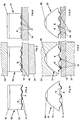
- the strip-like blank 1 is fed along the longitudinal direction 6 to a schematically illustrated rolling device 7 consisting of the rolls 4, 5, the contact strip 2 being fed in above the blank 1, while the coating strip 3 runs below the blank 1.
- a schematically illustrated rolling device 7 consisting of the rolls 4, 5, the contact strip 2 being fed in above the blank 1, while the coating strip 3 runs below the blank 1.
- the metal strip is brought into its shape with the final profile.
- the roll profiles of the subsequent rolling processes are designed such that the metal strip has an almost roof-shaped profile on its top, while its underside is provided with a predetermined number of projections.
- the number of protrusions is advantageously based on the width of the metal strip and the desired strength of the connection point between the contact carrier and the metal strip.
- the contact area created from the contact strip 2 is designated with the reference number 10 for the later working contact, while the coating area created on the projections 9 is designated with the reference number 11.
- the core area of the contact profile strand formed as metal strip 12, which is formed from the blank, is designated by reference number 13.
- the breakup of the metal strip 12 can be seen better on the basis of the cross section shown in FIG. 1c.
- the contact area 10 On the upper side of the triangular profile, the contact area 10 can be seen, for example, on the basis of a gold alloy or silver-palladium alloy, while the coating area 11, which is based on silver or a silver alloy, is plated on the projections 9.
- Nickel is predominantly used as the material for the blank, while the contact area 10 consists of a gold-silver alloy, for example AuAg 10, while the coating area 11 covering the projections 9 essentially consists of silver, ie of pure silver.
- the contact carrier tape is made of copper, but it is also possible to provide a copper alloy with a high copper content for the contact carrier tape.
- Figure 2 shows the metal strip 12 placed on the contact carrier 14, the coating 11 located on the projections 9 resting directly on the contact carrier strip and the back of the contact carrier strip 14 and the top of the metal strip 12 provided with the contact area 10 each from an electrode 21, 22 of the Welding circuit not shown here are included. From this figure it can be seen that the current density from the metal strip 12 increases increasingly in the area of the projections 9 in the direction of the contact carrier 14, which also results in an increasingly higher thermal output, so that the coating 11 is melted in the initial phase of the welding current pulse , whereupon the material of the coating is then pushed into the areas of the grooves 8 due to the pressing action of the electrodes 21, 22, where it forms an alloy with the copper of the contact carrier.
- FIG. 3 shows in cross section a contact profile strand after it has left the electrode device shown in FIG. 2 and is connected to the contact carrier strip underneath. It can be seen in a simple manner from FIG. 3 that the coating 11 originally located on the tips of the projections 9 has moved away from the projections 9 and in the interstices or grooves 8 together with the copper supplied by the contact carrier strip 14 one by one Melting process by means of resistance heating formed connection area between the contact carrier band 14 and metal band 12; During the welding process, the contact connection point designated by numeral 15 according to FIG.
- FIG. 4 shows a contact profile strand 12 with a multiplicity of projections, which is produced as a starting material by a similar method, and which is also provided with a coating 11 on its projections 9.
- FIG. 5 shows, according to FIG. 2, the metal strip 12 placed on contact carrier 14 according to FIG. 4 before the welding process; the two electrodes 21, 22 form, as already explained with reference to FIG. 2, part of the welding circuit.
- alloy regions 17 are formed between the projections, which consist of a silver-copper alloy with the proportions of approximately 72% by weight of silver and approximately 28% by weight of copper, and an electrical one Establish a conductive and firm mechanical connection between the contact profile strand from the metal strip 12 and the contact carrier strip 14.
Landscapes
- Engineering & Computer Science (AREA)
- Mechanical Engineering (AREA)
- Manufacturing & Machinery (AREA)
- Manufacture Of Switches (AREA)
- Contacts (AREA)
Applications Claiming Priority (2)
| Application Number | Priority Date | Filing Date | Title |
|---|---|---|---|
| DE4216224 | 1992-05-19 | ||
| DE4216224A DE4216224C2 (de) | 1992-05-19 | 1992-05-19 | Vormaterial und Halbzeug für elektrische Kontakte sowie Verfahren zur Herstellung |
Publications (3)
| Publication Number | Publication Date |
|---|---|
| EP0570662A2 true EP0570662A2 (fr) | 1993-11-24 |
| EP0570662A3 EP0570662A3 (fr) | 1994-04-20 |
| EP0570662B1 EP0570662B1 (fr) | 1996-09-04 |
Family
ID=6459045
Family Applications (1)
| Application Number | Title | Priority Date | Filing Date |
|---|---|---|---|
| EP93100769A Expired - Lifetime EP0570662B1 (fr) | 1992-05-19 | 1993-01-20 | Ebauche pour la production de contacts électriques, ainsi que fabrication et utilisation de l'ébauche |
Country Status (4)
| Country | Link |
|---|---|
| US (1) | US5421084A (fr) |
| EP (1) | EP0570662B1 (fr) |
| JP (1) | JP2545194B2 (fr) |
| DE (2) | DE4216224C2 (fr) |
Cited By (1)
| Publication number | Priority date | Publication date | Assignee | Title |
|---|---|---|---|---|
| EP0726613A3 (fr) * | 1995-02-09 | 1997-09-10 | Heraeus Gmbh W C | Ebauche et procédé pour la fabrication d'ébauches et de produits semi-finis pour des contacts électriques |
Families Citing this family (4)
| Publication number | Priority date | Publication date | Assignee | Title |
|---|---|---|---|---|
| DE4139998A1 (de) * | 1991-12-04 | 1993-06-09 | Siemens Ag, 8000 Muenchen, De | Kontaktstueck mit einer schaltsilber-kontaktauflage und verfahren zu seiner herstellung |
| FI100344B (fi) * | 1995-11-28 | 1997-11-14 | Ahlstrom Machinery Oy | Menetelmä lankaseulatuotteen valmistamiseksi ja lankaseulatuote |
| CN103104678B (zh) * | 2011-11-14 | 2015-07-01 | 上海交运汽车动力系统有限公司 | 一种自动变速器壳体及其焊接方法 |
| DE102019104318C5 (de) * | 2019-02-20 | 2023-06-22 | Auto-Kabel Management Gmbh | Elektrischer Leiter sowie Verfahren zur Herstellung eines elektrischen Leiters |
Family Cites Families (17)
| Publication number | Priority date | Publication date | Assignee | Title |
|---|---|---|---|---|
| US2181083A (en) * | 1936-01-02 | 1939-11-21 | Metals & Controls Corp | Laminated contact |
| US3147167A (en) * | 1962-01-17 | 1964-09-01 | Day Company | Method of producing electrical components |
| DE1464548A1 (de) * | 1962-04-05 | 1969-03-13 | Engelhard Ind Ltd | Elektrische Bimetallkontakte |
| US3346350A (en) * | 1965-05-25 | 1967-10-10 | Engelhard Ind Inc | Electrical contact tape |
| JPS52149353A (en) * | 1976-06-04 | 1977-12-12 | Mitsubishi Electric Corp | Method of welding nobleemetal contact material and metal material |
| JPS5448071A (en) * | 1977-09-21 | 1979-04-16 | Tanaka Precious Metal Ind | Method of manufacturing electrical contactor |
| JPS54133450A (en) * | 1978-04-10 | 1979-10-17 | Hitachi Ltd | Diffusion bonding method for different kind metal |
| DE2844888C2 (de) * | 1978-10-14 | 1983-02-24 | W.C. Heraeus Gmbh, 6450 Hanau | Vormaterial zur Herstellung elektrischer Kontakte |
| JPS55153686A (en) * | 1979-05-15 | 1980-11-29 | Tanaka Kikinzoku Kogyo Kk | Electrode for welding contact material |
| DE2922512A1 (de) * | 1979-06-01 | 1980-12-04 | Bihler Maschf Otto | Verfahren zum aufbringen grossflaechiger kontakte auf einen kontakttraeger sowie nach diesem verfahren hergestellte kontaktanordnung |
| DE2944613A1 (de) * | 1979-11-05 | 1981-05-07 | Inovan-Stroebe GmbH & Co KG, 7534 Birkenfeld | Verfahren zum herstellen eines profildrahtes |
| DE3107665A1 (de) * | 1981-02-28 | 1982-09-16 | W.C. Heraeus Gmbh, 6450 Hanau | "metallhalbzeug" |
| JPS607157A (ja) * | 1983-06-25 | 1985-01-14 | Masami Kobayashi | Ic用リ−ドフレ−ム |
| JPS6050819A (ja) * | 1983-08-31 | 1985-03-20 | 三菱電機株式会社 | 電気接触子 |
| DE3437981C2 (de) * | 1984-10-17 | 1986-08-21 | Doduco KG Dr. Eugen Dürrwächter, 7530 Pforzheim | Verfahren zum Herstellen eines Halbzeugs für elektrische Kontakte |
| ATE94684T1 (de) * | 1987-07-22 | 1993-10-15 | Siemens Ag | Kontakt zum hartloeten auf einem traeger mittels widerstandspressschweissung mittels eines kurzzeit-energieimpulses. |
| JPH01151114A (ja) * | 1987-12-08 | 1989-06-13 | Tanaka Kikinzoku Kogyo Kk | 複合電気接点材料 |
-
1992
- 1992-05-19 DE DE4216224A patent/DE4216224C2/de not_active Expired - Fee Related
-
1993
- 1993-01-20 DE DE59303619T patent/DE59303619D1/de not_active Expired - Fee Related
- 1993-01-20 EP EP93100769A patent/EP0570662B1/fr not_active Expired - Lifetime
- 1993-05-14 US US08/062,298 patent/US5421084A/en not_active Expired - Fee Related
- 1993-05-19 JP JP5117419A patent/JP2545194B2/ja not_active Expired - Lifetime
Cited By (2)
| Publication number | Priority date | Publication date | Assignee | Title |
|---|---|---|---|---|
| EP0726613A3 (fr) * | 1995-02-09 | 1997-09-10 | Heraeus Gmbh W C | Ebauche et procédé pour la fabrication d'ébauches et de produits semi-finis pour des contacts électriques |
| US5883352A (en) * | 1995-02-09 | 1999-03-16 | W.C. Heraeus Gmbh | Welding process |
Also Published As
| Publication number | Publication date |
|---|---|
| DE4216224A1 (de) | 1993-11-25 |
| US5421084A (en) | 1995-06-06 |
| JP2545194B2 (ja) | 1996-10-16 |
| EP0570662B1 (fr) | 1996-09-04 |
| JPH0668740A (ja) | 1994-03-11 |
| EP0570662A3 (fr) | 1994-04-20 |
| DE4216224C2 (de) | 1994-03-17 |
| DE59303619D1 (de) | 1996-10-10 |
Similar Documents
| Publication | Publication Date | Title |
|---|---|---|
| DE69815356T2 (de) | Verfahren zum herstellen einer lötkolbenspitze und hergestellte lötkolbenspitze dafür | |
| DE2710835A1 (de) | Vorrichtung zum anloeten oder anschweissen von anschlussdraehten an anschlusskontakten in halbleitervorrichtungen | |
| DE2844888A1 (de) | Vormaterial fuer elektrische kontakte | |
| DE19612164B4 (de) | Verfahren zum Verbinden eines Leiterdrahtes mit einem Anschluß und Vorrichtung dafür | |
| DE2920028A1 (de) | Elektrischer kontakt fuer einen schalter sowie verfahren zur herstellung eines solchen kontaktes | |
| DE69312196T2 (de) | Verfahren zur Vorbereitung der Montage eines Chips auf einem Substrat | |
| DE3005662C2 (de) | Verfahren zur Herstellung eines Kontaktelementes | |
| DE2143844A1 (de) | Verfahren zum herstellen von zweischichten-kontaktstuecken als formteil | |
| DE2517347A1 (de) | Kontaktkoerper und herstellungsverfahren hierzu | |
| DE3048242A1 (de) | Verfahren zur herstellung eines an ort und stelle mit einem traegermetall verschweissten zusammengesetzten elektrischen kontaktes sowie vorrichtung zur durchfuehrung des verfahrens | |
| EP0570662B1 (fr) | Ebauche pour la production de contacts électriques, ainsi que fabrication et utilisation de l'ébauche | |
| DE3785140T2 (de) | Verfahren zur herstellung einer verschweissten elektrischen kontaktanordnung. | |
| DE2747087A1 (de) | Zusammengesetztes material fuer elektrische kontakte | |
| DE3508806C2 (fr) | ||
| DE2259792A1 (de) | Elektrischer kontakt mit einem aus kupfer bestehenden grundkoerper und verfahren zur herstellung eines solchen | |
| DE2530704C3 (de) | Verbundwerkstoff als Halbzeug für elektrische Kontaktstucke und Herstellungsverfahren hierzu | |
| EP0726613B1 (fr) | Ebauche et procédé pour la fabrication d'ébauches et de produits semi-finis pour des contacts électriques | |
| DE2166925C3 (de) | Verfahren zum Herstellen von Zweischichten-Kontaktstücken als Formteil | |
| DE1187333B (de) | Elektrischer Kontakt mit grosser Schweisssicherheit, hoher Abbrandfestigkeit und guter Haftfestigkeit der Kontaktschicht auf dem Kontakttraeger | |
| EP0301218B1 (fr) | Procédé de jonction de pièces au moyen de chauffage par résistance au moyen d'une impulsion d'énergie de courte durée | |
| DE69704025T2 (de) | Verfahren zur herstellung eines elektromechanischen relais | |
| EP0300197B1 (fr) | Contact à souder par brasage fort sur un support au moyen de soudage par pression par résistance au moyen d'une impulsion d'énergie de courte durée | |
| DE102021102088B3 (de) | Verfahren zum Verbinden einer elektrischen Aluminiumleitung mit einem Anschlusselement aus einem artfremden Metallmaterial | |
| DE2649343A1 (de) | Vorrichtung und verfahren zur herstellung eines traegers fuer ein halbleiterbauelement | |
| DE29522396U1 (de) | Vormaterial zur Herstellung elektrischer Kontakte |
Legal Events
| Date | Code | Title | Description |
|---|---|---|---|
| PUAI | Public reference made under article 153(3) epc to a published international application that has entered the european phase |
Free format text: ORIGINAL CODE: 0009012 |
|
| 17P | Request for examination filed |
Effective date: 19930129 |
|
| AK | Designated contracting states |
Kind code of ref document: A2 Designated state(s): CH DE FR GB IT LI SE |
|
| PUAL | Search report despatched |
Free format text: ORIGINAL CODE: 0009013 |
|
| AK | Designated contracting states |
Kind code of ref document: A3 Designated state(s): CH DE FR GB IT LI SE |
|
| 17Q | First examination report despatched |
Effective date: 19950512 |
|
| GRAH | Despatch of communication of intention to grant a patent |
Free format text: ORIGINAL CODE: EPIDOS IGRA |
|
| GRAH | Despatch of communication of intention to grant a patent |
Free format text: ORIGINAL CODE: EPIDOS IGRA |
|
| GRAA | (expected) grant |
Free format text: ORIGINAL CODE: 0009210 |
|
| AK | Designated contracting states |
Kind code of ref document: B1 Designated state(s): CH DE FR GB IT LI SE |
|
| REG | Reference to a national code |
Ref country code: CH Ref legal event code: NV Representative=s name: KIRKER & CIE SA |
|
| GBT | Gb: translation of ep patent filed (gb section 77(6)(a)/1977) |
Effective date: 19960917 |
|
| REF | Corresponds to: |
Ref document number: 59303619 Country of ref document: DE Date of ref document: 19961010 |
|
| ITF | It: translation for a ep patent filed | ||
| ET | Fr: translation filed | ||
| PLAV | Examination of admissibility of opposition |
Free format text: ORIGINAL CODE: EPIDOS OPEX |
|
| PLBQ | Unpublished change to opponent data |
Free format text: ORIGINAL CODE: EPIDOS OPPO |
|
| PLBI | Opposition filed |
Free format text: ORIGINAL CODE: 0009260 |
|
| PLAV | Examination of admissibility of opposition |
Free format text: ORIGINAL CODE: EPIDOS OPEX |
|
| PLBF | Reply of patent proprietor to notice(s) of opposition |
Free format text: ORIGINAL CODE: EPIDOS OBSO |
|
| 26 | Opposition filed |
Opponent name: DODUCO GMBH Effective date: 19970604 |
|
| PLBF | Reply of patent proprietor to notice(s) of opposition |
Free format text: ORIGINAL CODE: EPIDOS OBSO |
|
| REG | Reference to a national code |
Ref country code: CH Ref legal event code: PFA Free format text: W.C. HERAEUS GMBH TRANSFER- W.C. HERAEUS GMBH & CO. KG |
|
| PLBO | Opposition rejected |
Free format text: ORIGINAL CODE: EPIDOS REJO |
|
| RAP2 | Party data changed (patent owner data changed or rights of a patent transferred) |
Owner name: W.C. HERAEUS GMBH & CO. KG |
|
| REG | Reference to a national code |
Ref country code: GB Ref legal event code: 732E |
|
| REG | Reference to a national code |
Ref country code: FR Ref legal event code: CJ |
|
| PLBN | Opposition rejected |
Free format text: ORIGINAL CODE: 0009273 |
|
| STAA | Information on the status of an ep patent application or granted ep patent |
Free format text: STATUS: OPPOSITION REJECTED |
|
| 27O | Opposition rejected |
Effective date: 19990606 |
|
| PGFP | Annual fee paid to national office [announced via postgrant information from national office to epo] |
Ref country code: GB Payment date: 20001212 Year of fee payment: 9 |
|
| PGFP | Annual fee paid to national office [announced via postgrant information from national office to epo] |
Ref country code: CH Payment date: 20001214 Year of fee payment: 9 |
|
| PGFP | Annual fee paid to national office [announced via postgrant information from national office to epo] |
Ref country code: SE Payment date: 20001227 Year of fee payment: 9 |
|
| PGFP | Annual fee paid to national office [announced via postgrant information from national office to epo] |
Ref country code: DE Payment date: 20010102 Year of fee payment: 9 |
|
| PGFP | Annual fee paid to national office [announced via postgrant information from national office to epo] |
Ref country code: FR Payment date: 20010103 Year of fee payment: 9 |
|
| REG | Reference to a national code |
Ref country code: GB Ref legal event code: IF02 |
|
| PG25 | Lapsed in a contracting state [announced via postgrant information from national office to epo] |
Ref country code: GB Free format text: LAPSE BECAUSE OF NON-PAYMENT OF DUE FEES Effective date: 20020120 |
|
| PG25 | Lapsed in a contracting state [announced via postgrant information from national office to epo] |
Ref country code: SE Free format text: LAPSE BECAUSE OF NON-PAYMENT OF DUE FEES Effective date: 20020121 |
|
| PG25 | Lapsed in a contracting state [announced via postgrant information from national office to epo] |
Ref country code: LI Free format text: LAPSE BECAUSE OF NON-PAYMENT OF DUE FEES Effective date: 20020131 Ref country code: CH Free format text: LAPSE BECAUSE OF NON-PAYMENT OF DUE FEES Effective date: 20020131 |
|
| PG25 | Lapsed in a contracting state [announced via postgrant information from national office to epo] |
Ref country code: DE Free format text: LAPSE BECAUSE OF NON-PAYMENT OF DUE FEES Effective date: 20020801 |
|
| EUG | Se: european patent has lapsed |
Ref document number: 93100769.4 |
|
| GBPC | Gb: european patent ceased through non-payment of renewal fee |
Effective date: 20020120 |
|
| REG | Reference to a national code |
Ref country code: CH Ref legal event code: PL |
|
| PG25 | Lapsed in a contracting state [announced via postgrant information from national office to epo] |
Ref country code: FR Free format text: LAPSE BECAUSE OF NON-PAYMENT OF DUE FEES Effective date: 20020930 |
|
| REG | Reference to a national code |
Ref country code: FR Ref legal event code: ST |
|
| PG25 | Lapsed in a contracting state [announced via postgrant information from national office to epo] |
Ref country code: IT Free format text: LAPSE BECAUSE OF NON-PAYMENT OF DUE FEES;WARNING: LAPSES OF ITALIAN PATENTS WITH EFFECTIVE DATE BEFORE 2007 MAY HAVE OCCURRED AT ANY TIME BEFORE 2007. THE CORRECT EFFECTIVE DATE MAY BE DIFFERENT FROM THE ONE RECORDED. Effective date: 20050120 |