EP0571142A1 - Photodiode à avalanche en silicium dopé au platine - Google Patents
Photodiode à avalanche en silicium dopé au platine Download PDFInfo
- Publication number
- EP0571142A1 EP0571142A1 EP93303751A EP93303751A EP0571142A1 EP 0571142 A1 EP0571142 A1 EP 0571142A1 EP 93303751 A EP93303751 A EP 93303751A EP 93303751 A EP93303751 A EP 93303751A EP 0571142 A1 EP0571142 A1 EP 0571142A1
- Authority
- EP
- European Patent Office
- Prior art keywords
- apd
- doped
- lifetime
- semiconductor layer
- exhibit
- Prior art date
- Legal status (The legal status is an assumption and is not a legal conclusion. Google has not performed a legal analysis and makes no representation as to the accuracy of the status listed.)
- Withdrawn
Links
- BASFCYQUMIYNBI-UHFFFAOYSA-N platinum Chemical compound [Pt] BASFCYQUMIYNBI-UHFFFAOYSA-N 0.000 title claims abstract description 46
- 229910052710 silicon Inorganic materials 0.000 title claims abstract description 22
- 239000010703 silicon Substances 0.000 title claims abstract description 22
- 229910052697 platinum Inorganic materials 0.000 title claims abstract description 21
- XUIMIQQOPSSXEZ-UHFFFAOYSA-N Silicon Chemical compound [Si] XUIMIQQOPSSXEZ-UHFFFAOYSA-N 0.000 title abstract description 20
- 239000004065 semiconductor Substances 0.000 claims abstract description 66
- 239000002019 doping agent Substances 0.000 claims abstract description 35
- 230000006798 recombination Effects 0.000 claims abstract description 19
- 230000001747 exhibiting effect Effects 0.000 claims description 4
- GYHNNYVSQQEPJS-UHFFFAOYSA-N Gallium Chemical compound [Ga] GYHNNYVSQQEPJS-UHFFFAOYSA-N 0.000 claims description 3
- 229910052733 gallium Inorganic materials 0.000 claims description 3
- 238000009377 nuclear transmutation Methods 0.000 claims description 3
- 239000000463 material Substances 0.000 description 32
- 239000010931 gold Substances 0.000 description 16
- PCHJSUWPFVWCPO-UHFFFAOYSA-N gold Chemical compound [Au] PCHJSUWPFVWCPO-UHFFFAOYSA-N 0.000 description 15
- 229910052737 gold Inorganic materials 0.000 description 15
- 238000005215 recombination Methods 0.000 description 13
- 238000010521 absorption reaction Methods 0.000 description 4
- 239000000969 carrier Substances 0.000 description 4
- 230000005284 excitation Effects 0.000 description 4
- 230000004907 flux Effects 0.000 description 4
- 230000001419 dependent effect Effects 0.000 description 3
- 238000002347 injection Methods 0.000 description 3
- 239000007924 injection Substances 0.000 description 3
- 230000004044 response Effects 0.000 description 3
- 238000004458 analytical method Methods 0.000 description 2
- 238000003491 array Methods 0.000 description 2
- 230000008901 benefit Effects 0.000 description 2
- 238000001514 detection method Methods 0.000 description 2
- 238000000034 method Methods 0.000 description 2
- 238000012986 modification Methods 0.000 description 2
- 230000004048 modification Effects 0.000 description 2
- 238000000926 separation method Methods 0.000 description 2
- 206010034960 Photophobia Diseases 0.000 description 1
- 230000002411 adverse Effects 0.000 description 1
- 230000003321 amplification Effects 0.000 description 1
- 230000015556 catabolic process Effects 0.000 description 1
- 230000008859 change Effects 0.000 description 1
- 230000002939 deleterious effect Effects 0.000 description 1
- 238000009792 diffusion process Methods 0.000 description 1
- 238000009826 distribution Methods 0.000 description 1
- 238000005516 engineering process Methods 0.000 description 1
- 239000003574 free electron Substances 0.000 description 1
- 239000012535 impurity Substances 0.000 description 1
- 208000013469 light sensitivity Diseases 0.000 description 1
- 238000004519 manufacturing process Methods 0.000 description 1
- 238000003199 nucleic acid amplification method Methods 0.000 description 1
- 238000005457 optimization Methods 0.000 description 1
- 230000008520 organization Effects 0.000 description 1
- 230000002028 premature Effects 0.000 description 1
- 230000008569 process Effects 0.000 description 1
- 230000035945 sensitivity Effects 0.000 description 1
- 239000007787 solid Substances 0.000 description 1
- 239000010409 thin film Substances 0.000 description 1
Images

Classifications
-
- H—ELECTRICITY
- H10—SEMICONDUCTOR DEVICES; ELECTRIC SOLID-STATE DEVICES NOT OTHERWISE PROVIDED FOR
- H10F—INORGANIC SEMICONDUCTOR DEVICES SENSITIVE TO INFRARED RADIATION, LIGHT, ELECTROMAGNETIC RADIATION OF SHORTER WAVELENGTH OR CORPUSCULAR RADIATION
- H10F30/00—Individual radiation-sensitive semiconductor devices in which radiation controls the flow of current through the devices, e.g. photodetectors
- H10F30/20—Individual radiation-sensitive semiconductor devices in which radiation controls the flow of current through the devices, e.g. photodetectors the devices having potential barriers, e.g. phototransistors
- H10F30/21—Individual radiation-sensitive semiconductor devices in which radiation controls the flow of current through the devices, e.g. photodetectors the devices having potential barriers, e.g. phototransistors the devices being sensitive to infrared, visible or ultraviolet radiation
- H10F30/22—Individual radiation-sensitive semiconductor devices in which radiation controls the flow of current through the devices, e.g. photodetectors the devices having potential barriers, e.g. phototransistors the devices being sensitive to infrared, visible or ultraviolet radiation the devices having only one potential barrier, e.g. photodiodes
- H10F30/225—Individual radiation-sensitive semiconductor devices in which radiation controls the flow of current through the devices, e.g. photodetectors the devices having potential barriers, e.g. phototransistors the devices being sensitive to infrared, visible or ultraviolet radiation the devices having only one potential barrier, e.g. photodiodes the potential barrier working in avalanche mode, e.g. avalanche photodiodes
-
- H—ELECTRICITY
- H10—SEMICONDUCTOR DEVICES; ELECTRIC SOLID-STATE DEVICES NOT OTHERWISE PROVIDED FOR
- H10F—INORGANIC SEMICONDUCTOR DEVICES SENSITIVE TO INFRARED RADIATION, LIGHT, ELECTROMAGNETIC RADIATION OF SHORTER WAVELENGTH OR CORPUSCULAR RADIATION
- H10F77/00—Constructional details of devices covered by this subclass
- H10F77/10—Semiconductor bodies
- H10F77/12—Active materials
- H10F77/122—Active materials comprising only Group IV materials
- H10F77/1223—Active materials comprising only Group IV materials characterised by the dopants
Definitions
- This invention relates generally to solid state light detection systems and more particularly to avalanche photodiodes.
- Photodiodes commonly used for converting light energy into corresponding electrical signals comprise one or more layers of photosensitive material doped to exhibit alternately p or n type conductivity, in which free holes and electrons are generated in response to incident light.
- the photosensitive material is a semiconductor and is disposed between electrodes.
- Dependent on device design free electrons or holes are predominantly collected at one or the other of the electrodes. The amount of charge collected is dependent (in part, at least) on the flux of the incident light, thus providing an electrical signal corresponding to the intensity of the incident light.
- Avalanche photodiodes are used to detect low intensity light and still produce electrical signals of sufficient magnitude to be readily used in most electrical processing circuitry.
- APDs exhibit an internal amplification of 10 to 500 times the original electrical signal generated solely by the absorption of the incident light.
- Desirable characteristics of an APD include high gain, low dark current (and related noise), and high switching speed, i.e., the ability to temporally discriminate between successive pulses of incident light.
- Gain is a function of the doping level of the material selected to form the APD and the biasing voltages applied to the particular APD structure.
- the level of dark current and switching speed in an APD depend on several characteristics of the semiconductor material used in fabricating the APD, namely the low-level lifetime, the high level lifetime, and the space charge lifetime of carriers in the photosensitive materials.
- Low level lifetime also known as minority carrier lifetime, refers to the excess minority carrier lifetime at low levels of injection, that is when there is little incident light and thus the concentration of injected carriers is a small fraction of the equilibrium majority carrier concentration.
- minority carrier lifetime is referred to as ⁇ po ; in a sufficiently p type semiconductor material it is referred to as ⁇ no .
- High level lifetime refers to the excess carrier lifetime at high level injection (i.e., high flux of incident light), when the injected carrier concentration is much larger than the equilibrium majority carrier concentration.
- the high level lifetime is the sum of ⁇ po and ⁇ no (the respective low level lifetimes for the for the n- and p-type semiconductors forming the p-n junction). Even in materials that exhibit multiple recombination levels, a single dominant recombination level is commonly used for analyzing the characteristics of the material.
- Space charge lifetime is the lifetime corresponding to charge generation in the space charge region (depletion layer) in a doped semiconductor material. Space charge lifetime is a function of the separation between the recombination level E r and the intrinsic level E i , and is given by E r - E i .
- the switching speed (i.e., the time it takes the charge resulting from the detection of a light pulse to "die down") of the device at low levels of light energy is determined by the low level lifetime of the photosensitive material. At higher levels of excitation, e.g., with a high flux of incident light energy, the switching speed is a function of the high level lifetime of the photosensitive material. Thus lower values of ⁇ po and ⁇ no indicate faster device switching speeds. Dark current is inversely proportional to the space charge generation lifetime.
- Intrinsic silicon doped to exhibit p or n type characteristics is typically used in making APDs as it is readily fabricated and integrated in arrays with associated processing circuitry, such as scan and data lines and thin film transistors.
- the minority carrier and high level lifetime of carriers in silicon are each relatively large and thus an APD in which the photosensitive material is substantially intrinsic silicon has relatively slow switching times.
- No lifetime-reducing dopants are currently used in fabricating silicon APDs because the increased dark current resulting when typical lifetime-reducing dopants are introduced in silicon would make the use of such a doped APD impractical. Minimization of dark current is a critical parameter in the APD art as the very nature of APDs and their employment to detect low light levels make any source of noise a critical detriment to APD operation.
- Gold is commonly used as a dopant in the power device art to modify the recombination characteristics of semiconductor materials used in devices such as thyristors.
- Use of gold as a deep level dopant modifies the recombination characteristics of carriers in silicon and improves switching speeds in the power device.
- the addition of gold increases the leakage current, but this typically is not of particular importance in a power device.
- Gold is not used as a dopant in APD technologies as the increased dark current severely degrades device performance.
- gold-doped semiconductor materials are electrically unstable at temperatures above about 150 ° C, and APDs are typically exposed to temperatures up to about 300° C in the fabrication process of arrays in which APDs are used.
- platinum doping provides reduced leakage at high temperatures, and exhibits different recombination lifetime values dependent on the level of injection.
- the advantage of platinum or gold in power devices is relative and depends on the particular employment of the device.
- features of this invention are to provide a silicon APD having fast switching times, an APD having fast switching times and with low dark current,and an APD exhibiting electrical stability at temperatures less than about 300°C.
- an avalanche photodiode includes a first semiconductor layer doped to exhibit p type conductivity and a second semiconductor absorption layer doped to exhibit n type conductivity.
- the first and second semiconductor absorption layers are disposed adjacent to one another to form a p-n junction.
- Each of the first and second semiconductor absorption layers have a carrier-lifetime reducing dopant distributed therethrough, the lifetime-reducing dopant exhibiting relatively large carrier cross-sections and causing each of the doped semiconductor layers to have at least one recombination center located between about 100 mV to 400 mV from the center of the bandgap.
- Platinum is advantageously used as the carrier-lifetime reducing dopant.
- platinum-doped semiconductor materials are electrically stable at temperatures less than about 300°C.
- the APD further includes a first conductive layer doped to exhibit p+ conductivity disposed over the surface of the first (p type) semiconductor layer opposite the surface of the first semiconductor layer forming the p-n junction, and a second conductive layer doped to exhibit n+ conductivity disposed over the surface of the second (n-type) semiconductor layer opposite the p-n junction.
- First and second contact pads are advantageously disposed respectively on the first and second conductive layers to provide electrical connections to components extemal to the APD.
- the sidewalls of the first and second semiconductor layers are typically beveled such that the sidewalls in the vicinity of the p-n junction have a curved contour.
- Figure 1 is a cross-sectional view of an APD fabricated in accordance with the present invention.
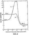
- Figure 2 is a graph representing the variation of carrier lifetime with the position of the Fermi energy level in each semiconductor layer doped with a lifetime-reducing dopant; curves representing relative single recombination center values for silicon doped with gold (Au) and silicon doped with platinum (Pt) are illustrated.
- FIG. 1 illustrates an avalanche photodiode (APD) 100 in accordance with the present invention.
- APD 100 comprises a first semiconductor layer 110 and a second semiconductor layer 120 which are adjacent to one another, forming a p-n junction 130 where the two materials adjoin or abut.
- APD 100 is oriented so that incident light beams 105 enter and are absorbed in first semiconductor layer 120.
- First semiconductor layer 110 advantageously comprises substantially intrinsic silicon and is doped with a dopant, such as gallium, to exhibit p type conductivity, and typically has a thickness of between about 20 ⁇ m and 100 ⁇ m.
- Second semiconductor layer 120 advantageously comprises substantially intrinsic silicon and is doped to exhibit n-type conductivity, and typically has a thickness between about 80 ⁇ m and 160 ⁇ m.
- Second semiconductor layer is advantageously neutron transmutation doped so that it exhibits the desired n-type conductivity.
- first and second semiconductor layers are entirely neutron transmutation doped to exhibit n type conductivity; a p type gallium dopant is then diffused into a portion of the wafer to form the first semiconductor layer exhibiting p type conductivity.
- Sidewalls 115, 125 of first and second semiconductor layers respectively further advantageously have a curved contour at least in the vicinity of p-n junction 130 in order to minimize premature breakdown and surface leakage in the device.
- APD 100 further comprises a first conductive layer 140 that is doped to exhibit p+ conductivity and is disposed over the surface of first semiconductor layer 110 that is opposite p-n junction 130. Dopants in first conductive layer 140 are also advantageously selected to provide the desired light sensitivity, for example blue sensitivity, for the incident light.
- a second conductive layer 150 is doped to exhibit n+ conductivity and is disposed over the surface of second semiconductor layer 120 opposite p-n junction 130.
- APD 100 is electrically coupled to components (not shown) for reading and recording charge produced in the APD in response to incident light by a first contact pad 160 in ohmic contact with first conductive layer 140 and by a second contact pad 170 in ohmic contact with second conductive layer 150.
- first and second semiconductor layers 110, 120 further include a carrier lifetime-reducing dopant.
- carrier lifetime-reducing refers to a dopant that reduces both the low-level lifetime and the high-level lifetime of the semiconductor material through which the dopant is distributed.
- the carrier lifetime-reducing dopant further exhibits deep levels having relatively large carrier cross-sections. The deep levels refer to the characteristic of the dopant, when distributed in the semiconductor layer, to have an energy level near the center of the bandgap.
- the carrier lifetime-reducing dopant is advantageously platinum (Pt).
- the platinum dopant is distributed through the semiconductor material, for example by diffusion, so as to have a selected dopant concentration in the range between about 1013 atoms/cm3 and 1016 atoms/cm3.
- the semiconductor material doped with the carrier lifetime reducing dopant has at least one recombination center located between about 100 mV and 400 mV from the center of the bandgap.
- both first and second semiconductor layers 110, 120 when doped in accordance with this invention, exhibit at least one recombination level between about 100 mV and 450 mV from the center of the energy bandgap for that layer. Typically only one recombination level is used in analysis even when multiple recombination levels occur.
- Platinum is advantageously used as the lifetime-reducing dopant as it improves APD performance in several ways.
- platinum doping provides much better performance than gold, which is the most common lifetime-reducing dopant used in the power device art.
- platinum reduces both high and low level carrier lifetimes while not adversely affecting the bulk leakage of the APD (therefore not increasing the dark current of the device).
- sufficient amounts of gold can reduce low and high level lifetimes, but only at the cost of higher bulk leakage from the device, which makes the device undesirable for use as a low leakage APD.
- the high level lifetime is a function of the sum of ⁇ po + ⁇ no , and thus the turn off at high levels of excitation is typically slower than at low levels of excitation.
- the ratio of the values of ⁇ po to ⁇ no for gold is about 1:100; thus, no matter how much gold is diffused or otherwise distributed through the silicon, the sum of the two lifetimes remains large and consequently results in relatively slow switching times in response to a high flux of incident light.
- the ratio of ⁇ po to ⁇ no for platinum is in the range of 1:1 to 1:10, and thus the turn off time at strong levels of excitation is faster in a platinum-doped device than in a gold-doped device.
- first and second semiconductor layer 110, 120 The distribution of platinum through first and second semiconductor layer 110, 120 to the selected dopant concentration further results in a higher space charge lifetime than that of a gold doped semiconductor material. Consequently, bulk leakage, which is inversely proportional to the space charge lifetime, is much less for a platinum doped semiconductor material than for a gold doped semiconductor material.
- the graph of Figure 2 illustrates representative curves for gold and platinum, showing representative relative magnitudes of ⁇ po and ⁇ no and illustrates the difference in space charge lifetime for a semiconductor material doped with gold and doped with platinum.
- space charge lifetime is determined by E r - E i for the doped material (i.e., the separation in between the recombination level and the intrinsic level).
- E r - E i for gold is approximately zero; thus gold-doped semiconductor material exhibits lower space charge lifetimes and higher bulk leakage than platinum-doped semiconductor material.
- Platinum-doped semiconductor materials are additionally electrically stable (i.e., the electrical characteristics of the doped material do not change markedly in this temperature range) at temperatures up to about 300°C, whereas gold-doped semiconductor material becomes electrically unstable at temperatures about 150 ° C.
Landscapes
- Light Receiving Elements (AREA)
Applications Claiming Priority (2)
| Application Number | Priority Date | Filing Date | Title |
|---|---|---|---|
| US88444392A | 1992-05-18 | 1992-05-18 | |
| US884443 | 1992-05-18 |
Publications (1)
| Publication Number | Publication Date |
|---|---|
| EP0571142A1 true EP0571142A1 (fr) | 1993-11-24 |
Family
ID=25384639
Family Applications (1)
| Application Number | Title | Priority Date | Filing Date |
|---|---|---|---|
| EP93303751A Withdrawn EP0571142A1 (fr) | 1992-05-18 | 1993-05-14 | Photodiode à avalanche en silicium dopé au platine |
Country Status (2)
| Country | Link |
|---|---|
| EP (1) | EP0571142A1 (fr) |
| JP (1) | JPH0637349A (fr) |
Cited By (3)
| Publication number | Priority date | Publication date | Assignee | Title |
|---|---|---|---|---|
| WO2001018882A1 (fr) * | 1999-09-06 | 2001-03-15 | Abb Ab | Dispositif de commutation |
| EP1435666A3 (fr) * | 2002-12-10 | 2008-12-31 | General Electric Company | Photodiode à avalanche utilisable dans des environnements hostiles |
| CN104882510A (zh) * | 2015-06-04 | 2015-09-02 | 镇江镓芯光电科技有限公司 | 一种新型小倾角半台面结构的碳化硅雪崩光电二极管 |
Families Citing this family (1)
| Publication number | Priority date | Publication date | Assignee | Title |
|---|---|---|---|---|
| JP5196327B2 (ja) | 2008-12-22 | 2013-05-15 | 山一電機株式会社 | 半導体装置用ソケット |
Citations (2)
| Publication number | Priority date | Publication date | Assignee | Title |
|---|---|---|---|---|
| GB1215557A (en) * | 1968-07-30 | 1970-12-09 | Nippon Electric Co | A semiconductor photosensitive device |
| US5021854A (en) * | 1987-12-03 | 1991-06-04 | Xsirius Photonics, Inc. | Silicon avalanche photodiode array |
-
1993
- 1993-05-14 EP EP93303751A patent/EP0571142A1/fr not_active Withdrawn
- 1993-05-17 JP JP5113519A patent/JPH0637349A/ja active Pending
Patent Citations (2)
| Publication number | Priority date | Publication date | Assignee | Title |
|---|---|---|---|---|
| GB1215557A (en) * | 1968-07-30 | 1970-12-09 | Nippon Electric Co | A semiconductor photosensitive device |
| US5021854A (en) * | 1987-12-03 | 1991-06-04 | Xsirius Photonics, Inc. | Silicon avalanche photodiode array |
Non-Patent Citations (4)
| Title |
|---|
| APPLIED PHYSICS LETTERS. vol. 30, no. 2, 15 January 1977, NEW YORK US pages 118 - 120 GELEZUNAS ET AL. 'UNIFORM LARGE-AREA HIGH-GAIN SILICON AVALANCHE RADIATION DETECTORS FROM TRANSMUTATION DOPED SILICON' * |
| MATERIALS RESEARCH SOCIETY SYMPOSIA PROCEEDINGS vol. 27, 1984, NEW-YORK,US pages 537 - 542 MOGRO-CAMPERO ET AL. 'CARRIER LIFETIME REDUCTION BY ION IMPLANTATION INTO SILICON' * |
| NUCLEAR INSTRUMENTS AND METHODS vol. 196, 1982, HOLLAND pages 143 - 148 KIM ET AL. 'NEUTRON TRANSMUTATION DOPED SILICON DETECTORS' * |
| RADIATION PROTECTION DOSIMETRY -ENVIRONMENTAL AND HUMAN RISKS OF TRITIUM-PROCEEDINGS OF A WORKSHOP vol. 16, no. 1/2, 17 February 1986, KARLSRUHE, FRG pages 527 - 530 DIXON ET AL. 'GOLD AND PLATINUM DOPED RADIATION RESISTANT SILICON DIODE DETECTORS' * |
Cited By (4)
| Publication number | Priority date | Publication date | Assignee | Title |
|---|---|---|---|---|
| WO2001018882A1 (fr) * | 1999-09-06 | 2001-03-15 | Abb Ab | Dispositif de commutation |
| EP1435666A3 (fr) * | 2002-12-10 | 2008-12-31 | General Electric Company | Photodiode à avalanche utilisable dans des environnements hostiles |
| KR101025186B1 (ko) | 2002-12-10 | 2011-03-31 | 제너럴 일렉트릭 캄파니 | 거친 환경에 사용하기 위한 애벌런치 포토다이오드 |
| CN104882510A (zh) * | 2015-06-04 | 2015-09-02 | 镇江镓芯光电科技有限公司 | 一种新型小倾角半台面结构的碳化硅雪崩光电二极管 |
Also Published As
| Publication number | Publication date |
|---|---|
| JPH0637349A (ja) | 1994-02-10 |
Similar Documents
| Publication | Publication Date | Title |
|---|---|---|
| Cook et al. | Electron and hole impact ionization coefficients in InP determined by photomultiplication measurements | |
| Chu et al. | Thermionic injection and space‐charge‐limited current in reach‐through p+ np+ structures | |
| EP0142316A2 (fr) | Photodiodes p-i-n et à avalanche | |
| EP0625803A1 (fr) | Structure de photodiode | |
| US5016073A (en) | Photodetector semiconductor which does not require extensive cooling | |
| EP0473197A1 (fr) | Dispositif photosenseur | |
| Manoliu et al. | P n junctions in polycristalline-silicon films | |
| US6326654B1 (en) | Hybrid ultraviolet detector | |
| US5304824A (en) | Photo-sensing device | |
| US4599632A (en) | Photodetector with graded bandgap region | |
| JPS60244078A (ja) | 広いバンドギヤツプキヤツプ層を有する背面照明形フオトダイオード | |
| KR950004550B1 (ko) | 수광소자 | |
| EP0242298A2 (fr) | Photodiode à avalanche | |
| EP1470574B9 (fr) | Photodiode pin à grande vitesse avec une sensibilité améliorée | |
| KR20020005990A (ko) | 반도체 장치 | |
| EP0522746A1 (fr) | Dispositif photodétecteur semi-conducteur | |
| US4553155A (en) | High speed bias-free photodetector | |
| US20030087466A1 (en) | Phototransistor device | |
| US4831428A (en) | Infrared ray detection device | |
| US4833512A (en) | Heterojunction photo-detector with transparent gate | |
| US4750025A (en) | Depletion stop transistor | |
| JPH0637349A (ja) | プラチナをドープしたアバランシェフォトダイオード | |
| US4567430A (en) | Semiconductor device for automation of integrated photoarray characterization | |
| US5710448A (en) | Integrated polysilicon diode contact for gain memory cells | |
| US4416051A (en) | Restoration of high infrared sensitivity in extrinsic silicon detectors |
Legal Events
| Date | Code | Title | Description |
|---|---|---|---|
| PUAI | Public reference made under article 153(3) epc to a published international application that has entered the european phase |
Free format text: ORIGINAL CODE: 0009012 |
|
| AK | Designated contracting states |
Kind code of ref document: A1 Designated state(s): DE GB NL |
|
| STAA | Information on the status of an ep patent application or granted ep patent |
Free format text: STATUS: THE APPLICATION IS DEEMED TO BE WITHDRAWN |
|
| 18D | Application deemed to be withdrawn |
Effective date: 19940525 |