EP0571673B1 - Haltbare Beschichtung für elektrische Steckkontakte - Google Patents
Haltbare Beschichtung für elektrische Steckkontakte Download PDFInfo
- Publication number
- EP0571673B1 EP0571673B1 EP92304731A EP92304731A EP0571673B1 EP 0571673 B1 EP0571673 B1 EP 0571673B1 EP 92304731 A EP92304731 A EP 92304731A EP 92304731 A EP92304731 A EP 92304731A EP 0571673 B1 EP0571673 B1 EP 0571673B1
- Authority
- EP
- European Patent Office
- Prior art keywords
- palladium
- layer
- gold
- plated
- terminal
- Prior art date
- Legal status (The legal status is an assumption and is not a legal conclusion. Google has not performed a legal analysis and makes no representation as to the accuracy of the status listed.)
- Expired - Lifetime
Links
Images

Classifications
-
- C—CHEMISTRY; METALLURGY
- C25—ELECTROLYTIC OR ELECTROPHORETIC PROCESSES; APPARATUS THEREFOR
- C25D—PROCESSES FOR THE ELECTROLYTIC OR ELECTROPHORETIC PRODUCTION OF COATINGS; ELECTROFORMING; APPARATUS THEREFOR
- C25D5/00—Electroplating characterised by the process; Pretreatment or after-treatment of workpieces
- C25D5/10—Electroplating with more than one layer of the same or of different metals
-
- H—ELECTRICITY
- H01—ELECTRIC ELEMENTS
- H01R—ELECTRICALLY-CONDUCTIVE CONNECTIONS; STRUCTURAL ASSOCIATIONS OF A PLURALITY OF MUTUALLY-INSULATED ELECTRICAL CONNECTING ELEMENTS; COUPLING DEVICES; CURRENT COLLECTORS
- H01R13/00—Details of coupling devices of the kinds covered by groups H01R12/70 or H01R24/00 - H01R33/00
- H01R13/02—Contact members
- H01R13/03—Contact members characterised by the material, e.g. plating, or coating materials
-
- Y—GENERAL TAGGING OF NEW TECHNOLOGICAL DEVELOPMENTS; GENERAL TAGGING OF CROSS-SECTIONAL TECHNOLOGIES SPANNING OVER SEVERAL SECTIONS OF THE IPC; TECHNICAL SUBJECTS COVERED BY FORMER USPC CROSS-REFERENCE ART COLLECTIONS [XRACs] AND DIGESTS
- Y10—TECHNICAL SUBJECTS COVERED BY FORMER USPC
- Y10T—TECHNICAL SUBJECTS COVERED BY FORMER US CLASSIFICATION
- Y10T29/00—Metal working
- Y10T29/49—Method of mechanical manufacture
- Y10T29/49002—Electrical device making
- Y10T29/49117—Conductor or circuit manufacturing
- Y10T29/49204—Contact or terminal manufacturing
- Y10T29/49224—Contact or terminal manufacturing with coating
Definitions
- This invention relates to electrical contact terminals having layers of noble metal electrodeposited thereon.
- Electrical contact terminals used in the electronic industry must be good electrical conductors, highly reliable under repeated use, and at the same time be resistant to corrosion or oxidation. Traditionally, the industry has met these criteria by plating the terminals with hard gold. The accelerating price of gold, however, has encouraged the industry to find less expensive means while maintaining the desired characteristics.
- palladium instead of gold has been explored by the industry. Although palladium has been found to be a good conductor, corrosion resistant and less expensive than gold, palladium has been found to be unreliable for terminals that require repeated matings. Depending upon which of the many known palladium plating baths was used, repeated mating of the plated contact terminals either wore through the palladium layer or caused the palladium layer to crack and abrade the surface of the mating parts. Either type of problem causes the contact terminals to fail.
- the disclosed invention solves the above problems by the discovery that the internal macrostress within the palladium layer itself is the cause of the problems.
- the internal macrostress of the palladium is measured by X-ray defraction according to the procedure described by C.N.J. Wagner et al, Trans. Mat. Soc. AIME 233 , 1280(1965).
- the plated palladium has a low internal macrostress, less than 206.84 MPa (30,000 psi) (low stress palladium)
- the palladium layer wears out through adhesive wear after a few matings.
- Palladium having high internal macrostress greater than 965.27 MPa (140,000 psi), fractures when subjected to repeated matings, causing abrasive wear.
- Plating baths which deposit palladium having a macrostress in the range of 30,000 to 140,000 psi (medium stress palladium) produce contact terminals which exhibit much greater wear characteristics than contacts plated with low or high stress palladium.
- a small number of the medium stress palladium contact terminals show early wear and spontaneously exhibit macrocracks. This problem with the medium stress palladium is prevented and the wear characteristics of these palladium plated contact terminals are unexpectedly and surprisingly increased by the application of a layer of pure soft gold.
- the gold used preferably meets MIL SPEC MIL-G-45204B Type III Grade A, Gold percentage 99.9, Knoop maximum 90.
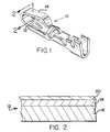
- FIGURE 1 is a three dimensional view of an electrical contact terminal which has been plated according to the invention.
- FIGURE 2 is a cross-sectional view of the plated area of the terminal taken along the lines 2-2 of Figure 1.
- FIGURE 3 is a micrograph of a cross-section of the plated contact zone of the terminal of Figure 1 showing the layers of plating on the terminal, the magnification being 10,000 times.
- An AMR scanning electron microscope with Kavex Line X-Ray Fluorescence Detector was used.
- FIGURE 4 is a surface view of the plated contact zone of the terminal of Figure 1, the magnification being 1000 times.
- an electrical contact terminal 10 has a contact zone 12 with a plated surface 14.
- a cross-sectional view of the contact zone 12 shows the substratum 16 of terminal 10, the layer of plated palladium 18 and the layer of gold 20 on the palladium layer 18.
- Figure 3 also being a micrograph of a cross-section of the contact zone 12 of a terminal 10 plated according to the invention, shows the relative thickness of the layer of plating on the substratum 16.
- the gold layer 20 is obviously much thinner than the palladium layer 18.
- Figure 4 is a surface view of a plated contact terminal 10, at a magnification of 1000. The picture shows that the plated contact area is free from microcracks.
- the entire surface of terminals may be plated according to the disclosed invention. It is more economical, however, to selectively plate only the contact zone of the terminals with palladium and gold. If selective plating is desired, the terminal receives an underplating of nickel in order to protect all the areas of the terminal that are not later protected by palladium and gold.
- the substratum of the contact terminal is initially plated with a strike of noble metal, gold, silver or palladium, preferably palladium, in order to promote adhesion of the subsequent palladium and gold layers.
- a palladium strike unlike a gold or silver strike is indistinguishable from the subsequent palladium layer when viewed with an electron microscope, as in Figure 3.
- the use of noble metal strikes for adhesion is well known by those skilled in the art. Numerous plating baths, as known in the art, can be used for producing these strikes.
- One bath for plating palladium within the desired macrostress range is disclosed in U.S. Patent 1,970,950.
- the bath contains an aqueous solution of Pd(NO2) 4 -2 , in an amount sufficient to provide a palladium concentration from about 5,01 to 30,40 g/l (0.61 to 3.7 troy ounces per gallon).
- the bath is operated at a temperature ranging from 45 - 75°C (113° to 167°F), a pH ranging from 4.5 to 7.5, and a current density of 10,8 mA/cm (10 amperes per square foot).
- the gold preferably is at least 99.9% pure and must have a Knoop hardness in the range of 60 to 90.
- the gold being soft acts as a contact lubricant as the terminals are subjected to repeated matings. Any gold plating bath that meets MIL SPEC MIL-G45204B Type III, Grade A, Gold percentage 99.9, Knoop maximum 90, can be used to plate the gold layer.
- a hard gold flash over palladium has none of these attributes. This combination behaves in a similar manner to the bare palladium deposit by exhibiting adhesive wear and also early brittle fracture of the deposit.
- a wear testing device consisting of a flat reciprocating lower surface and a stationary hemispherical upper surface or terminal was used to determine the durability of plated terminals. The device measures both frictional forces and contact resistance. See Rabinowitz, Friction and Wear of Materials , John Wiley and Sons, Inc., New York, 1965, p. 104, for a similar device.
- Terminals were mounted in the device.
- the durability of the contact surface was determined by applying a 0.2 kg (0.44 pound) load to the terminal to simulate typical contact force and subjecting the loaded terminal to the reciprocating motion of the device, each cycle of the device representing one insertion and one withdrawal of the terminal.
- the number of completed cycles was counted until base metal was exposed, the plated surface exhibited microcracks, or a predetermined number of cycles was achieved.
- a number of terminals of the type illustrated in Figure 1 were plated in the preferred manner.
- the phosphor bronze substrate of the terminal was first plated with 2,54 ⁇ m (100 microinches) of nickel using a nickel sulfamate (chloride free) bath. See George A. DiBari, 49th Guidebook, Metal Finishing , p. 278, 1981, Metals and Plastics Publications, Inc., Hackensack, New Jersey.
- a strike of palladium to aid the adherence of the subsequent palladium layer was then applied.
- the commercial Decorex plating bath was used. This bath is available from Sel-Rex, Nutley, New Jersey 07110. The bath was operated at 24°C (75°F), a pH of 9, and a current density of 10,8 mA cm ⁇ (10 amperes per square foot).
- the terminals were then plated with 72 microinches of medium stress palladium using the bath as described in U.S. Patent No. 1,970,950.
- the palladium concentration was 10,02 g/l (1.22 troy ounces per gallon).
- the bath was operated at a temperature of 60°C (140°F), a pH of 6.0, and a current density of 10,8 mA cm ⁇ (10 amperes per square foot).
- the terminals were then plated with about 0,09 ⁇ m (3.7 microinches) of soft gold.
- the bath used for these samples contained an aqueous solution of KAu(CN)2 in an amount sufficient to provide a gold concentration of 8,21 g/l (1 troy ounce per gallon).
- the bath was operated at 60°C (140°F), pH 6.2, and a current density of 5 5,4 mA cm ⁇ (amperes per square foot).
- the residual macrostress of these terminals ranged from 551.58 to 896.32 MPa (80,000 to 130,000 psi). In the durability tests, all of the samples completed 1000 cycles without exhibiting failure. A few samples were subjected to further testing for durability and reached 10,000 cycles without failure. The contact resistance of terminals plated with medium stress palladium and soft gold was not affected by exposure to 249°C (480°F) for 16 hours.
- a number of terminals of the type illustrated in Figure 1 were plated with nickel, palladium strike, and palladium in the same manner as those in Example 1. No soft gold was plated on these samples.
- the macrostress of the medium stress palladium on these samples ranged from 413.69 to 965.27 MPa (60,000 to 140,000 psi). Over ninety per cent of these terminals failed to complete 50 cycles in the durability test.
- Terminals of the type illustrated in Figure 1 were plated with nickel and a palladium strike as previously described in Example 1.
- the terminals were then plated with 1.90 ⁇ m (75 microinches) of palladium using the commercially available Pallaflex bath.
- This bath is available from Vanguard Research Associates, Inc., South Plainfield, New Jersey 07080.
- the bath was operated at 65°C (149°F), a pH of 6.8, and a current density of 10,8 mA cm ⁇ (10 amperes per square foot). 0.08 ⁇ m (three microinches) of soft gold was plated over the palladium layer using the same gold bath as Example 1.
- the residual macrostress in the sample tested was 89.63 MPa (13,000 psi).
- the contact surface of this terminal failed at less than 10 cycles in the durability test.
- Terminals of the type illustrated in Figure 1 were plated with nickel and a palladium strike as previously described in Example 1.
- the terminals were then plated with 1.90 ⁇ m (75 microinches) of palladium using the commercially available Pallaspeed bath.
- This bath is available from Technic, Inc., Cranston, Rhode Island 02910.
- the bath was operated at 60°C (149°F), a pH of 5.8, and a current density of 10,8 mA cm ⁇ (10 amperes per square foot). 0.08 ⁇ m (three microinches) of soft gold was plated over the palladium layer using the same gold bath as Example 1.
- the residual macrostress of the samples tested was in the range of 965.27 to 1 103.16 MPa (140,000 to 160,000 psi). Durability testing of samples in this range gave erratic results. Some of the samples failed after two cycles, some after ten cycles, and some survived 1000 cycles.
- terminals plated according to the herein disclosed invention have a substantial and unexpected increase in durability.
Landscapes
- Chemical & Material Sciences (AREA)
- Engineering & Computer Science (AREA)
- Chemical Kinetics & Catalysis (AREA)
- Electrochemistry (AREA)
- Materials Engineering (AREA)
- Metallurgy (AREA)
- Organic Chemistry (AREA)
- Electroplating Methods And Accessories (AREA)
- Contacts (AREA)
Claims (8)
- Verfahren zum Herstellen eines beschichteten elektrischen Kontaktanschlusses (10) zum Zusammenfügen mit einem komplementären Kontaktglied, mit den Schritten: Auswählen eines elektrischen Kontaktanschlusses (10), Auswählen einer Palladium-Beschichtungslösung und Auswählen von Prozeßparametern für das Beschichten von Palladium aus einem Bad der gewählten Lösung auf den elektrischen Kontaktanschluß, Aufbringen einer Schicht (18) aus Palladium aus dem Bad auf den Anschluß und Aufbringen einer Schicht (20) aus Gold auf die Palladiumschicht, wobei das Gold eine Knoop-Härte im Bereich von 60 bis 90 hat, wobei das Verfahren durch folgende Schritte gekennzeichnet ist:- Auswählen der Palladium-Beschichtungslösung und Optimieren der Parameter so, daß die Palladium-Schicht (18) des damit beschichteten Anschlusses (10) durchgehend ein Niveau der inneren Makrobeanspruchung von wenigstens 206,84 MPa (30.000 psi) und bis zu etwa 965,27 MPa (140.000 psi) hat und Auswählen der Gold-Beschichtungslösung, wodurch- das Vorhandensein einer solchen wesentlichen Makrobeanspruchungs-Charakteristik der aufgebrachten Palladium-Schicht (18) die Dauerhaftigkeit des Kontaktanschlusses wesentlich erhöht.
- Verfahren nach Anspruch 1, bei dem die Makrobeanspruchung der Palladium-Schicht (18) im Bereich von 275,79 bis 896,32 MPa (40.000 bis 130.000 psi) liegt.
- Verfahren nach Anspruch 1 oder 2, bei dem die Palladium-Schicht (18) eine Dicke zwischen 0,13 und 2,54 µm, vorzugsweise 0,38 bis 2,03 µm (5 bis 100 Mikrozoll, vorzugsweise 15 bis 80 Mikrozoll) hat.
- Verfahren nach Anspruch 1, 2 oder 3, bei dem das Gold wenigstens zu 99,9 Prozent rein ist.
- Verfahren nach einem vorhergehenden Anspruch, bei dem die Goldschicht (20) innerhalb des Bereiches von 0,03 bis 0,18 µm, vorzugsweise 0,05 bis 0,10 µm (1 bis 7 Mikrozoll, vorzugsweise 2 bis 4 Mikrozoll) liegt.
- Elektrischer Kontaktanschluß (10) mit erhöhter Dauerhaftigkeit, der dazu bestimmt ist, ein komplementäres Kontaktglied zu berühren und damit einen elektrischen Kontakt herzustellen, wobei der Anschluß (10) ein Substrat (16) mit einer darauf aufgebrachten zweischichtigen Beschichtung hat, dadurch gekennzeichnet, daß- die erste Schicht (18) der Beschichtung aus Palladium besteht, das auf das Substrat (16) aufgebracht ist, wobei die Palladium-Schicht eine Makrobeanspruchung im Bereich von 206,84 bis 965,27 MPa, vorzugsweise 413,69 bis 689,48 MPa (30.000 bis 140.000 psi, vorzugsweise 60.000 bis 100.000 psi) hat, und- die zweite Schicht (20) aus Gold besteht, das auf das Palladium aufgebracht ist, wobei die Goldbeschichtung vorzugsweise eine Knoop-Härte im Bereich von 60 bis 90 hat.
- Anschluß (10) nach Anspruch 6, bei dem die Palladium-Schicht (18) eine Dicke zwischen 0,13 und 2,54 µm, vorzugsweise 0,38 bis 2,03 µm (5 bis 100 Mikrozoll, vorzugsweise 15 bis 80 Mikrozoll) hat.
- Anschluß (10) nach Anspruch 6 oder 7, bei dem die Goldschicht (20) im Bereich von 0,03 bis 0,18 µm, vorzugsweise 0,05 bis 0,10 µm (1 bis 7 Mikrozoll, vorzugsweise 2 bis 4 Mikrozoll) liegt.
Applications Claiming Priority (3)
| Application Number | Priority Date | Filing Date | Title |
|---|---|---|---|
| US44494082A | 1982-11-29 | 1982-11-29 | |
| US82808486A | 1986-02-07 | 1986-02-07 | |
| US44915989A | 1989-12-15 | 1989-12-15 |
Publications (2)
| Publication Number | Publication Date |
|---|---|
| EP0571673A1 EP0571673A1 (de) | 1993-12-01 |
| EP0571673B1 true EP0571673B1 (de) | 1996-01-03 |
Family
ID=27412229
Family Applications (1)
| Application Number | Title | Priority Date | Filing Date |
|---|---|---|---|
| EP92304731A Expired - Lifetime EP0571673B1 (de) | 1982-11-29 | 1992-05-26 | Haltbare Beschichtung für elektrische Steckkontakte |
Country Status (4)
| Country | Link |
|---|---|
| US (1) | US5129143A (de) |
| EP (1) | EP0571673B1 (de) |
| DE (1) | DE69207384T2 (de) |
| ES (1) | ES2081567T3 (de) |
Families Citing this family (28)
| Publication number | Priority date | Publication date | Assignee | Title |
|---|---|---|---|---|
| US5208978A (en) * | 1992-05-07 | 1993-05-11 | Molex Incorporated | Method of fabricating an electrical terminal pin |
| US5308252A (en) * | 1992-12-24 | 1994-05-03 | The Whitaker Corporation | Interposer connector and contact element therefore |
| US7073254B2 (en) | 1993-11-16 | 2006-07-11 | Formfactor, Inc. | Method for mounting a plurality of spring contact elements |
| US20020053734A1 (en) | 1993-11-16 | 2002-05-09 | Formfactor, Inc. | Probe card assembly and kit, and methods of making same |
| AU5964196A (en) * | 1995-05-26 | 1996-12-11 | Formfactor, Inc. | Spring element electrical contact and methods |
| US5994152A (en) | 1996-02-21 | 1999-11-30 | Formfactor, Inc. | Fabricating interconnects and tips using sacrificial substrates |
| US8033838B2 (en) | 1996-02-21 | 2011-10-11 | Formfactor, Inc. | Microelectronic contact structure |
| US5722861A (en) * | 1996-02-28 | 1998-03-03 | Molex Incorporated | Electrical connector with terminals of varying lengths |
| JPH10134869A (ja) * | 1996-10-30 | 1998-05-22 | Yazaki Corp | 端子材料および端子 |
| GB2349391A (en) * | 1999-04-27 | 2000-11-01 | Mayfair Brassware Limited | Outer gold coated article |
| JP3551411B2 (ja) * | 1999-10-27 | 2004-08-04 | 常木鍍金工業株式会社 | 接点部材及びその製造方法 |
| JP2002298938A (ja) * | 2001-03-30 | 2002-10-11 | Jst Mfg Co Ltd | 樹脂ハンダを用いたツイストペアケーブルの電気コネクタ及びこの電気コネクタへの電線接続方法 |
| JP2002298946A (ja) * | 2001-03-30 | 2002-10-11 | Jst Mfg Co Ltd | 樹脂ハンダを用いた電気接続具、電気コネクタ及びこれらへの電線接続方法 |
| JP2002298993A (ja) * | 2001-03-30 | 2002-10-11 | Jst Mfg Co Ltd | 片方に樹脂ハンダを用いた一対の電気コネクタ |
| JP2002298940A (ja) | 2001-03-30 | 2002-10-11 | Jst Mfg Co Ltd | 樹脂ハンダを用いた電気接触子、電気コネクタ及びこれらのプリント配線板への接続方法 |
| JP2002298962A (ja) * | 2001-03-30 | 2002-10-11 | Jst Mfg Co Ltd | 樹脂ハンダを用いた電気接触子、電気コネクタ及びこれらのプリント配線板への接続方法 |
| JP2002298995A (ja) | 2001-03-30 | 2002-10-11 | Jst Mfg Co Ltd | 樹脂ハンダを用いた同軸ケーブルの結束部材及び同軸ケーブルの電気コネクタ並びに結束部材の同軸ケーブル又は電気コネクタへの接続方法 |
| US6793544B2 (en) * | 2003-02-05 | 2004-09-21 | General Motors Corporation | Corrosion resistant fuel cell terminal plates |
| US7352601B1 (en) * | 2003-11-24 | 2008-04-01 | Michael Paul Minneman | USB flash memory device |
| US8314355B2 (en) * | 2005-05-20 | 2012-11-20 | Mitsubishi Electric Corporation | Gas insulated breaking device |
| JP2007180009A (ja) * | 2005-12-02 | 2007-07-12 | Ngk Spark Plug Co Ltd | 圧着端子及び当該圧着端子を備えたガスセンサ及び前記圧着端子の製造方法 |
| US8721855B2 (en) * | 2005-12-02 | 2014-05-13 | Ngk Spark Plug Co. Ltd. | Crimp contact, crimp contact with an electrical lead, gas sensor including said crimp contact and method for manufacturing said gas sensor |
| JP5079605B2 (ja) * | 2008-06-30 | 2012-11-21 | 株式会社オートネットワーク技術研究所 | 圧着端子及び端子付電線並びにこれらの製造方法 |
| EP2960999B1 (de) * | 2013-02-22 | 2018-03-21 | Furukawa Electric Co., Ltd. | Endgerät, drahtverbindungsstruktur und verfahren zur herstellung des endgeräts |
| EP2843087B1 (de) * | 2013-02-24 | 2017-04-19 | Furukawa Electric Co., Ltd. | Metallelement, anschlussklemme, elektrische drahtverbindungsstruktur und verfahren zur herstellung einer anschlussklemme |
| DE102014222679A1 (de) * | 2014-11-06 | 2016-05-12 | Robert Bosch Gmbh | Kontaktieranordnung für eine Ader eines elektrischen Kabels |
| CN106400068A (zh) * | 2016-11-29 | 2017-02-15 | 江苏澳光电子有限公司 | 一种用于接线端子表面电镀的渡液及其应用 |
| WO2021188674A1 (en) | 2020-03-18 | 2021-09-23 | Xtalic Corporation | Nanostructured palladium-based alloys and related methods |
Family Cites Families (7)
| Publication number | Priority date | Publication date | Assignee | Title |
|---|---|---|---|---|
| US1904241A (en) * | 1926-12-31 | 1933-04-18 | Kammerer Erwin | Compound metal stock |
| US1970950A (en) * | 1932-06-20 | 1934-08-21 | Int Nickel Co | Electrodeposition of platinum metals |
| US2846649A (en) * | 1952-09-26 | 1958-08-05 | Ampatco Lab Corp | Electrical connector |
| US2897584A (en) * | 1957-05-22 | 1959-08-04 | Sel Rex Corp | Gold plated electrical contact and similar elements |
| DE2540943B2 (de) * | 1975-09-13 | 1978-02-02 | W.C. Heraeus Gmbh, 6450 Hanau | Kontaktkoerper fuer einen elektrischen steckkontakt |
| US4435253A (en) * | 1983-01-28 | 1984-03-06 | Omi International Corporation | Gold sulphite electroplating solutions and methods |
| EP0140619B1 (de) * | 1983-10-14 | 1993-03-17 | Hitachi Chemical Co., Ltd. | Anisotrop elektrisch leitender Klebefilm und Verfahren zum Verbinden von Schaltungen unter dessen Anwendung |
-
1990
- 1990-09-10 US US07/581,261 patent/US5129143A/en not_active Expired - Fee Related
-
1992
- 1992-05-26 ES ES92304731T patent/ES2081567T3/es not_active Expired - Lifetime
- 1992-05-26 EP EP92304731A patent/EP0571673B1/de not_active Expired - Lifetime
- 1992-05-26 DE DE69207384T patent/DE69207384T2/de not_active Expired - Fee Related
Also Published As
| Publication number | Publication date |
|---|---|
| DE69207384D1 (de) | 1996-02-15 |
| ES2081567T3 (es) | 1996-03-16 |
| EP0571673A1 (de) | 1993-12-01 |
| US5129143A (en) | 1992-07-14 |
| DE69207384T2 (de) | 1996-08-01 |
Similar Documents
| Publication | Publication Date | Title |
|---|---|---|
| EP0571673B1 (de) | Haltbare Beschichtung für elektrische Steckkontakte | |
| US5066550A (en) | Electric contact | |
| US8101285B2 (en) | Metallic material for a connecting part and a method of producing the same | |
| US6755958B2 (en) | Barrier layer for electrical connectors and methods of applying the layer | |
| EP2009656A1 (de) | Elektrisches kontaktmaterial und herstellungsverfahren dafür | |
| EP1352993A1 (de) | Metallplattiertes material und herstellungsverfahren dafür und diese verwendende elektrische und elektronische teile | |
| KR100440363B1 (ko) | 적합한니켈코팅및이러한니켈코팅으로물품을코팅하기위한방법 | |
| EP1081251B1 (de) | Elektrolytisch abgeschiedener Edelmetallüberzug, der abriebfeste Partikel enthält | |
| US5679471A (en) | Silver-nickel nano-composite coating for terminals of separable electrical connectors | |
| EP0214667A1 (de) | Elektrolytische Niederschläge aus Palladium und einer Palladium enthaltenden Legierung und Verfahren zu ihrer Herstellung | |
| JP3551411B2 (ja) | 接点部材及びその製造方法 | |
| JP3519727B1 (ja) | コネクタ端子およびそれを有するコネクタ | |
| Antler | Tribology of metal coatings for electrical contacts | |
| Cohen et al. | Development of silver‐palladium alloy plating for electrical contact applications | |
| Antler et al. | Sliding wear of inlay clad metals and electrodeposited cobalt-gold | |
| Lindborg et al. | Intermetallic growth and contact resistance of tin contacts after aging | |
| JP2005068445A (ja) | 金属被覆された金属部材 | |
| US4925407A (en) | Nickel-based electrical contact | |
| JPH08167442A (ja) | パラジウムめっき電気コンタクト | |
| US4518469A (en) | Method of making non-precious metal electrical contacts by electroplating | |
| EP0531099A2 (de) | Hochtemperaturfeste Korrosionbeständige Kontakte oder elektrische Verbinder und Verfahren zu ihrer Herstellung | |
| JPH043041B2 (de) | ||
| JP3561504B2 (ja) | ステンレス鋼製導電性部材及びその製造方法 | |
| CA1260099A (en) | Nickel-based electrical contact device | |
| Fairweather | Alloy gold deposits for electronic applications: An evaluation of the gold-copper-cadmium sulphite system |
Legal Events
| Date | Code | Title | Description |
|---|---|---|---|
| PUAI | Public reference made under article 153(3) epc to a published international application that has entered the european phase |
Free format text: ORIGINAL CODE: 0009012 |
|
| AK | Designated contracting states |
Kind code of ref document: A1 Designated state(s): DE ES GB IT NL |
|
| 17P | Request for examination filed |
Effective date: 19940519 |
|
| 17Q | First examination report despatched |
Effective date: 19940118 |
|
| GRAA | (expected) grant |
Free format text: ORIGINAL CODE: 0009210 |
|
| AK | Designated contracting states |
Kind code of ref document: B1 Designated state(s): DE ES GB IT NL |
|
| ITF | It: translation for a ep patent filed | ||
| REF | Corresponds to: |
Ref document number: 69207384 Country of ref document: DE Date of ref document: 19960215 |
|
| REG | Reference to a national code |
Ref country code: ES Ref legal event code: FG2A Ref document number: 2081567 Country of ref document: ES Kind code of ref document: T3 |
|
| PLBE | No opposition filed within time limit |
Free format text: ORIGINAL CODE: 0009261 |
|
| STAA | Information on the status of an ep patent application or granted ep patent |
Free format text: STATUS: NO OPPOSITION FILED WITHIN TIME LIMIT |
|
| 26N | No opposition filed | ||
| PGFP | Annual fee paid to national office [announced via postgrant information from national office to epo] |
Ref country code: NL Payment date: 19990322 Year of fee payment: 8 |
|
| PG25 | Lapsed in a contracting state [announced via postgrant information from national office to epo] |
Ref country code: NL Free format text: LAPSE BECAUSE OF NON-PAYMENT OF DUE FEES Effective date: 20001201 |
|
| NLV4 | Nl: lapsed or anulled due to non-payment of the annual fee |
Effective date: 20001201 |
|
| REG | Reference to a national code |
Ref country code: GB Ref legal event code: IF02 |
|
| PGFP | Annual fee paid to national office [announced via postgrant information from national office to epo] |
Ref country code: GB Payment date: 20050518 Year of fee payment: 14 |
|
| PGFP | Annual fee paid to national office [announced via postgrant information from national office to epo] |
Ref country code: ES Payment date: 20050609 Year of fee payment: 14 |
|
| PGFP | Annual fee paid to national office [announced via postgrant information from national office to epo] |
Ref country code: DE Payment date: 20050630 Year of fee payment: 14 |
|
| PG25 | Lapsed in a contracting state [announced via postgrant information from national office to epo] |
Ref country code: GB Free format text: LAPSE BECAUSE OF NON-PAYMENT OF DUE FEES Effective date: 20060526 |
|
| PG25 | Lapsed in a contracting state [announced via postgrant information from national office to epo] |
Ref country code: ES Free format text: LAPSE BECAUSE OF NON-PAYMENT OF DUE FEES Effective date: 20060527 |
|
| PGFP | Annual fee paid to national office [announced via postgrant information from national office to epo] |
Ref country code: IT Payment date: 20060531 Year of fee payment: 15 |
|
| PG25 | Lapsed in a contracting state [announced via postgrant information from national office to epo] |
Ref country code: DE Free format text: LAPSE BECAUSE OF NON-PAYMENT OF DUE FEES Effective date: 20061201 |
|
| GBPC | Gb: european patent ceased through non-payment of renewal fee |
Effective date: 20060526 |
|
| REG | Reference to a national code |
Ref country code: ES Ref legal event code: FD2A Effective date: 20060527 |
|
| PG25 | Lapsed in a contracting state [announced via postgrant information from national office to epo] |
Ref country code: IT Free format text: LAPSE BECAUSE OF NON-PAYMENT OF DUE FEES Effective date: 20070526 |