EP0572151A2 - Varistoren mit gesputterten Anschlüssen und Methode zur Aufbringung von gesputterten Anschlüssen auf Varistoren - Google Patents
Varistoren mit gesputterten Anschlüssen und Methode zur Aufbringung von gesputterten Anschlüssen auf Varistoren Download PDFInfo
- Publication number
- EP0572151A2 EP0572151A2 EP93303816A EP93303816A EP0572151A2 EP 0572151 A2 EP0572151 A2 EP 0572151A2 EP 93303816 A EP93303816 A EP 93303816A EP 93303816 A EP93303816 A EP 93303816A EP 0572151 A2 EP0572151 A2 EP 0572151A2
- Authority
- EP
- European Patent Office
- Prior art keywords
- varistors
- components
- row
- varistor
- sputtering
- Prior art date
- Legal status (The legal status is an assumption and is not a legal conclusion. Google has not performed a legal analysis and makes no representation as to the accuracy of the status listed.)
- Withdrawn
Links
Images


Classifications
-
- H—ELECTRICITY
- H01—ELECTRIC ELEMENTS
- H01C—RESISTORS
- H01C17/00—Apparatus or processes specially adapted for manufacturing resistors
- H01C17/006—Apparatus or processes specially adapted for manufacturing resistors adapted for manufacturing resistor chips
-
- H—ELECTRICITY
- H01—ELECTRIC ELEMENTS
- H01C—RESISTORS
- H01C1/00—Details
- H01C1/14—Terminals or tapping points specially adapted for resistors; Arrangements of terminals or tapping points on resistors
-
- H—ELECTRICITY
- H01—ELECTRIC ELEMENTS
- H01C—RESISTORS
- H01C7/00—Non-adjustable resistors formed as one or more layers or coatings; Non-adjustable resistors made from powdered conducting material or powdered semi-conducting material with or without insulating material
- H01C7/10—Non-adjustable resistors formed as one or more layers or coatings; Non-adjustable resistors made from powdered conducting material or powdered semi-conducting material with or without insulating material voltage responsive, i.e. varistors
- H01C7/102—Varistor boundary, e.g. surface layers
Definitions
- This invention relates generally to varistors and a method of sputtering terminations on varistors and like electrical components, and more particularly to multilayer ceramic varistors with sputtered terminations and methods of applying sputtered terminations to a plurality of varistors and like components in a single operation.
- Varistors or voltage-dependent nonlinear resistors have been used as, among other things, surge absorbing elements, arresters and voltage stabilizer elements. Varistors typically employ single layer disk-shape ceramic bodies having voltage-dependent nonlinearity. Multilayer varistors became available in the market in 1988. The preparation and typical composition of this type of varistor is described in detail in U.S. Pat. No. 4,290,041 to Utsumi et al. which is incorporated herein by reference.
- the varistor may comprise a semiconducting block-shaped body made up of conducting grains separated by voltage sensitive grain boundaries. After formation of the varistor's ceramic body it is necessary to "terminate” the varistor, that is, to apply conductive coatings to the exposed electrode portions of the varistor. This permits the varistor to be readily connected to a printed circuit board or the like.
- termination is obtained by applying paste to the portions of the ceramic body having exposed electrodes.
- the paste may comprise a low melt glass frit and a conductive material such as silver or a silver alloy. After application of the paste, the varistor is heated to drive off solvents and/or binders and to fuse the glass including the silver to the ceramic body.
- the terminated varistors may have electrical leads soldered to them or be used as surface mount devices.
- the terminating compound can be very costly if palladium, platinum, and/or other noble metals are added to improve leach resistance.
- the cost of the added materials can be ten times or more than that of silver alone. Improving leach resistance is necessary as nickel-plated terminations have become an industrial standard for surface-mount components.
- a plurality of varistors already terminated and fired with silver terminations may be placed in a plating basket in a known technique for plating ceramic capacitors.
- the basket is then immersed in a plating solution. After sufficient metal has been deposited, the basket is removed from the plating solution and the varistors are cleaned.
- This plating operation has a number of drawbacks.
- One difficulty resides in the fact that the varistor is a semiconductor made up of conducting grains separated by voltage sensitive grain boundaries. This sensitivity to voltage change subjects the varistor to "creepage" during the plating process. Creepage is the phenomena where plating covers not only the end portions of the body (as it is supposed to), but begins to plate or "creep" from the end portions across the entire body from end to end. Of course, when the creepage reaches from end to end shorting occurs and the varistor is useless. This problem can be eliminated by applying an insulating compound such as a plastic binder over the areas where plating is not desired. However, this requires an added step to the process and adds to the manufacturing costs. Furthermore, the plating solution is generally acidic and will gradually etch the ceramic body if contact is made during plating.
- Sputtering is advantageous in that it is possible to deposit extremely thin layers of metallic material with the assurance that all portions subjected to the deposition procedure will be intimately engaged by the deposited metal. Thus, only the entire end portion of the. varistor will be contacted by the termination material. Thus, sputtering achieves favorable results over the plating of varistors with less problems and at a much lower cost.
- the termination materials still resides in that the deposited increments of metal will be received by all exposed portions of the varistor.
- the side faces of the varistor that is, the faces between the ends to which terminations are to be applied are completely shielded from the sputtering operation, there is substantial likelihood of forming a film of sputtered material extending between the ends of the varistor, thereby short-circuiting the varistor.
- the applicant has used several techniques for sputtering terminations on varistors.
- One technique for effecting sputtered termination of varistors is the "close-pack method.”
- sputter termination is applied by fitting a plurality of varistors into a specially formed metallic jig or die which so closely embraces the sides of the varistors as to preclude the formation of a film of sputtered material on the side-faces of the varistors during metal deposition.
- the surrounding ceramic bodies adjacent to a particular body provide the "mask" for the side faces of that body.
- this method requires that the fabrication of the bodies and the loading of the die be of precise dimensions capable of handling large quantities of varistors in a single run.
- Another technique is to sputter the terminations on the ceramic bodies while shielding the portions of the varistors which are to remain free of sputtered material by implanting the varistors in an elastomeric block or slab having apertures sized to intimately engage side portions of the varistors while exposing their ends.
- This technique is described in detail as being applicable to capacitors in U.S. Pat. No. 4,561,954 to Scrantom et al. (“Scrantom”) which is incorporated herein by reference.
- Scrantom permits the manufacture of "lands,” terminated end portions which cover not only the ends of the capacitors but extend slightly along the side margins of the capacitors.
- Scrantom is useful for applying terminations to the ends of varistors, but limits the number of varistors that can-be terminated at a time since the elastomeric mask occupies a significant portion of the area where additional varistors could be located in the close-pack method.
- the present invention provides for varistors having sputtered terminations and a method of terminating varistors as well as other types of electrical components by an improved sputtering process.
- the invention provides for masking the electrical components during sputtering with high density packing. Additionally, if desired, the invention permits for the manufacture of "lands" on the varistors or components without sacrificing much space where additional varistors could be placed as required by a conventional masking method.
- a method for readily masking varistors to enable the application of sputter terminations combines the advantages of the close spacing of parts of the close-pack method as well as the advantages available under a conventional masking method.
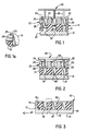
- FIG. 1 is a diagrammatic fragmentary sectional view of portions of the loading mechanism and mask during initial stages of loading of varistors into the mask.
- FIG. 1a is a magnified fragmentary view of a portion of the apparatus illustrated in FIG. 1.
- FIG. 2 is a section similar to FIG. 1 showing the position of the loading assembly components after the varistors have been inserted into position within the mask member.
- FIG. 3 is a fragmentary sectional view of the mask inserted in a jig or frame adapted to be introduced into the sputtering apparatus.
- FIG. 4 is a perspective view on a smaller scale of the filled jig or frame assembly ready to be introduced into the sputtering apparatus, with portions of the apparatus cut-away to show interior detail.
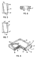
- FIG. 5 is a side elevation view of a sputter terminated varistor.
- FIG. 6 is a fragmentary view of a varistor mounted in a mask in accordance with an embodiment of the invention.
- FIG. 7 is a terminated varistor formed in accordance with the embodiment shown in FIG. 6.
- FIG. 8 is a partial perspective view of a preferred arrangement of rows of varistors alternating with spacing strips in a frame.
- the spacing strips mask the row faces of the varistors.
- the adjacent varistors mask the column faces of the adjacent varistors within that row.
- FIG. 9 is a fragmentary close-up sectional view of a holding bar.
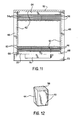
- FIG. 10 is a plan view of a loading device which includes a frame for holding the varistors in place during the sputtering process.
- FIG. 11 is a plan view of a fully loaded plate (varistors in middle portion of plate not shown) which shows a frame, a plate and a retainer.
- FIG. 12 is a perspective view of a sputtered varistor with a sputtered end and two-sided lands.
- FIG. 4 is a perspective view of a fixture or assembly for introduction into a sputtering apparatus.
- the fixture includes a bottom frame portion 11 and an upper frame component 12.
- the bottom frame 11 comprises a base portion 13 and a surrounding side wall portion 14.
- the upper frame component 12 includes a side wall portion 15 and an inwardly directed lip portion 16.
- the frame encompasses a mask 17 formed of an elastomeric material.
- SILASTIC is sold under the registered trademark SILASTIC and manufactured by the Dow Corning Corporation of Midland, Mich.
- SILASTIC comprises a silicone rubber.
- a preferred grade for the application is J RTV Silicone Rubber.
- Alternative silicone rubber compositions may also be used.
- the mask 17 as shown in FIGS. 1, 2 and 3, includes a plurality of apertures 18 of a size which intimately embrace varistors 19 which are to be terminated at their opposite ends 20 and 21.
- varistors 19 are manufactured in a manner which causes the electrodes to be exposed at one or the other of the end faces 20 or 21. It is the function of a termination to connect all of the electrodes. The terminations also function as an anchor point for leads or the like so the varistor can be introduced into an electrical circuit.
- FIGS. 1 and 2 illustrate an apparatus for introducing the varistors into the apertures 18 in the mask 17.
- each mask may desirably include thousands of apertures.
- a load plate 22 which is provided with a plurality of apertures 23 corresponding in number and position with the apertures 18 of the mask 17.
- the apertures 23 of the load plate include tapered or funnel like lead portions 24 of a size significantly larger than the cross-section of the varistors 19, the lead portion 24 merging with a guide portion 25 and finally a discharge portion 26.
- the dimensions of the guide portion 25 are slightly larger than the cross-sectional dimensions of the varistor and function to guide the varistors into the discharge portion 26, which latter portion is sized to closely correspond with the cross-sectional dimensions of the varistors.
- the load plate 22 may be filled by placing the plate beneath a bulk supply of varistors, the plate being vibrated or reciprocated in a horizontal plane for a period of time during which period varistors are caused by the vibratory movement to enter into the various apertures 23. After a period of oscillation or vibration beneath the bulk supply, the plate 22 is removed and continuously caused to vibrate. After a period of time the varistors will have reached positions wherein one or the other of the end portions 20 or 21 will have progressed at least into the guide portion 25 of the apertures 23 of the load plate.
- the filled load plate 22 is thereafter superposed over mask 17 in a fixture.
- the fixture is provided with a back-up plate 27 disposed beneath mask 17.
- the fixture is disposed within a loading jig assembly which includes a pusher grid 28 having a plurality of depending pusher rods 29 spaced to register with the apertures 23 of the load plate.
- the pusher grid 28 is thereafter shifted down so as to force the varistors out of the load plate 22 and into the apertures 18 of the mask 17.
- the pusher grid 28 is disclosed as having descended part way down such that the lower terminal ends 21 of the varistors have been caused to enter part way into the elastomeric mask 17.
- the grid 28 is shifted to its lowermost position with the result that the varistors 19 have been advanced into the mask 17 such that the upper and lower ends 20, 21 of the varistors are in substantial co-planar alignment with the upper and lower surfaces 30, 31 of the mask 17. Due to the elasticity and deformability of the mask 17 the varistors will be retained by friction of the mask in the position noted.
- the flexibility of the mask enables the varistors to be forced into this position despite a slightly imperfect alignment of the lower ends 21 of the varistors with the uppermost ends of the apertures 18. Where such slight misalignment occurs the downward pressure on the varistors is sufficient to deform the mask whereby the downwardly moving varistor is forced into the slightly misaligned aperture in the mask.
- the filled mask is mounted within the fixture as best illustrated in FIG. 4.
- the "out-gasing" problem can be solved by subjecting the mask 17, prior to loading, to a sputtering step to deposit a thin metallic film over the surfaces 30, 31 of the mask.
- the thickness of the film may be no more than a tenth of a micron or less, and functions to preclude out-gasing.
- Subsequent sputtering steps can be carried out whereby a pure metallic layer will cover both exposed ends of the varistors and the predeposited film. This is diagrammatically illustrated at 32 in FIG. 1a.
- both the upper and lower surfaces 30 and 31 of the mask are subjected to the pre-sputtering step. After a sputter coating is effected over one of the surfaces 30 the mask is removed from the fixture and inverted so that a subsequent sputtering operation covers the surface 31 as well as the varistor ends 21 which are exposed when the mask is inverted.
- the varistors are removed from the apertures by a pusher grid assembly similar to grid 28.
- the grid assembly includes pusher rods which enter into the aligned apertures of the mask and drive the finished varistors from the apertures 18.
- the mask may be refilled and reused without a prior pre-sputtering step, since the mask will include a metal coating comprised of the initial pre-sputtered coating as well as the over sputtering deposited on the surfaces of the mask by the sputtering procedure employed to terminate the varistors.
- the mask may be reused until the coating or build up on the surface of the mask renders the mask unduly stiff or resistant to deformation, following which it is necessary to chemically remove the metallic build-up from the surfaces of the mask, subject the mask to a further pre-sputtering step, and thereafter repeat the cycle.
- FIG. 5 There is shown in FIG. 5 a finished varistor 19 having upper and lower surfaces 20 and 21 to which have been applied metallic layers 33, 34, respectively. Lead members may be soldered to the terminations 33, 34 by any of a number of conventional procedures.
- FIG. 7 a varistor is shown which is similar to that shown in FIG. 5.
- the varistor of FIG. 7 differs from that of FIG. 5 in that the termination portions 33', 34' cover not only the ends' 20', 21' of the varistor 19', but also extend slightly along the side margins of the varistor. These structural features are referred to as "lands.”
- the embodiment of FIG. 7 is fabricated by loading the varistors 19' into a mask 17' so that the upper and lower surfaces (only the upper surface being shown in FIG. 6) project slightly beyond the upper and lower margins of the mask 17'. This condition is achieved by using a mask of slightly lesser thickness than the length of the varistors and by introducing a slightly compressible layer between the undersurface of the mask 17' and load plate 27.
- the pusher rods 29 will force the lower ends of varistors 19' through the body of the mask 17' so that they indent slightly into the compressible layer. Both ends of the varistors will then project slightly above and below the upper and lower surfaces of the mask 17'.
- the masking method permits the manufacture of lands a feature which is not obtainable with the next method.
- sputter termination is applied by fitting a plurality of varistors into a specially formed metallic jig or die which so closely embraces the sides of the varistors as to preclude the formation of a film of sputtered material on the side-faces of the varistors during metal deposition.
- the surrounding ceramic bodies adjacent to a particular body provide the "mask" for the side faces of that body.
- the method maximizes efficiency in sputtering the parts by using all of the available space within the jig or die because it does not include a mask between parts.
- One aspect of the invention provides a preferred method combining the high manufacturing efficiency of the close-pack method. Additionally, if desired, the preferred method can provide for the formation of lands like the elastomeric masking method discussed earlier yet avoid the loss of useful area in the die for processing additional varistors. As will be seen, the method is not limited to applying terminations to varistors, but can be also used to apply terminations to other electrical components. For the sake of brevity, however, the method will be discussed in the context of sputtering terminations on varistors.
- the invention provides a varistor loading device 40 including a movable frame 42.
- the frame 42, a bottom plate 73 and a closing bar 75 (FIG. 11) attached after loading is completed serve to hold the varistors 44 during the sputtering process.
- the frame 42 is square or rectangular-shaped. However, in contrast to the previous methods, the frame 42 changes dimensions during the loading sequence.
- FIG. 11 illustrates that the frame 42 may be made up of two holding bars 46, 48, a movable bar 64 and a closing bar 75.
- the holding bars 46, 48 are parallel to one another.
- the sliding bar 64 and closing bar 75 are also parallel to one another.
- Each holding bar 46, 48 is connected at one of their ends to the stop bar 52 where the movable bar 64 rests when the plate is fully loaded forming a three-sided "fixed" portion of the frame 42.
- the closing bar 75 is the "fourth side" of the frame 42.
- the two holding bars 46, 48 of the frame 42 are in a fixed relationship during the loading and sputtering process, whereas the movable bar 64 moves incrementally with each push of the push bar 50 during the loading sequence.
- the rows of varistors 44 are loaded into the frame 42 in predetermined lengths.
- the rows are oriented during the loading process so that they are parallel to the stop bar 52 and the push bar 50 and are confined at their ends 54, 56 by the holding bars 46, 48.
- the stop bar 52 will function to confine the total number of rows which can be loaded into the frame 42 as explained in the following discussion.
- the varistors 44 are packed transverse to the frame 42 so that only their ends 58 where the termination is to be applied is exposed.
- the varistors 44 are block-shaped, and serve as "masks” for their adjacent varistors 44 along the "column-face.”
- a spacing strip 60 masks the "row face" of the varistors 44.
- the method provides that each row of varistors 44 is separated from the adjacent rows by spacing strips 60.
- the varistors 44 are loaded in the frame 42 for sputtering in the following manner (FIG. 10).
- a spacing loader 62 disposed above the frame 42 inserts a rectangular-shaped spacing strip 60 in front of the "open portion" of the frame 42 so that the strip 60 rests against a sliding bar 64 located in the frame 42 and parallel to the push bar 50.
- Each end of the strip 60 is initially held in a feed-in slot 66, 68 in each holding bar 46, 48.
- the strip 60 is held in a groove 70 in the holding bars 46, 48 (FIG. 9).
- the strip 60 rests against the sliding bar 64.
- a varistor feeder located over the frame 42 feeds a row of varistors 44 into the frame 42 next to the strip 60.
- the row alignment device 72 packs the varistor row tightly together (from right to left) so that there are no "gaps" in the row.
- the push bar 50 pushes the row of varistors 44, the strip 60, the sliding bar 64 as a "single unit” an incremental distance (i.e., one row width) into the frame 42.
- the row of varistors 44 are held together as a unit at their ends by the parallel holding bars 46, 48, and by the push bar 50 and the sliding bar 64.
- the push bar 50 moves back out of the frame and the spacing loader 62 inserts another strip 60 next to the row of varistors 44 just inserted.
- the process is then repeated until the entire frame 42 is filled with varistors 44, that is, when the sliding bar 64 contacts the stop bar 52 and can proceed no further.
- the closing bar 75 and the retainer 74 are attached (FIG. 11).
- the resulting assembly is then transported to a suitable work space for sputtering of the terminations of the varistors 44.
- the spacing strip 60 is rectangular- shaped and has a width which equals the end to end dimension or length of the varistors 44.
- the spacing strip 60 is made of rigid plastic.
- any other materials of similar or greater rigidity such as metal may also be suitable.
- the spacing strips can be omitted so that a true close-pack arrangement is achieved.
- the spacing strip 60 has a width slightly less than the length of the varistor 44. This latter embodiment permits the formation of terminations extending beyond the end faces of the varistors creating the so-called "lands" (FIG. 12). Thus, the end portions may optionally project slightly beyond the spacing material or may be flush with the spacing material.
- the varistors Prior to loading, the varistors are cleaned utilizing a conventional freon type decreasing compound and are thermally etched for approximately an hour at 810°C.
- the loaded and precoated fixtures described are sputter coated by passing the same beneath the target of a sputtering device.
- an in-line sputtering system such as a system identified as the SERIES 900 SPUTTERING DEVICE as manufactured by MATERIALS RESEARCH CORPORATION of Orangeberg, N.Y., may be employed.
- An in-line sputtering system is preferred in that it permits the fixtures to be progressively advanced beneath target areas of different compositions whereby a layer of a first sputter deposited material may be formed directly over the exposed surface and thereafter a second and if desired a third layer applied.
- a thin chromium layer (0.01 to 0.1 ⁇ m) may be applied for adhesion.
- a thin layer nickel or nickel vanadium layer (0.1 to 2 ⁇ m) and a final silver or tin layer (1 to 15 ⁇ m).
- the nickel layer provides a barrier against leaching of the silver layer when electrical connections are soldered to the terminations of the varistors.
- the assembly is placed in a vacuum load lock which is pumped to a pressure of less than 50 X 10-5 torr and thereafter introduced into the main sputtering chamber.
- Sputtering may be effected at a power level of 4.2 kilowatts and scan speed of approximately millimeters per second across the target area. Sputtering is performed preferably in an argon gas environment at a pressure of 10 X 10-5 torr. Where a chromium substrate is used for a high adhesion layer, thicknesses in the range of 0.04 to 0.08 micrometers are preferred. A nickel coating of from 0.4 to 1.0 micrometers has been found to be optimum. Where a silver or palladium overcoating is to be employed a coating thickness of 1 micron has been found sufficient.
- a separate plate 73 is attached to the frame 42 and the retainer 74 by screws and the whole assembly is flipped over. The top plate is then removed and the opposite ends may be sputtered.
- the precoating of the surfaces of mask 17 may be applied by using a chromium target material.
- the coating thickness is non-critical, but is initially in the range of about 0.15 micrometers.
- the initial chromium presputter coating will be oversputtered in the course of treating varistors and thus will increase significantly in thickness after being used for a series of varistor sputtering cycles.
- varistors of the multilayer type whereby a plurality of varistors may be simultaneously and effectively treated.
- a mask of 4 inches by 4 inches may carry over thirteen hundred "1206 style" varistors for simultaneous treatment in an elastomeric frame, 5700 varistors in a plastic lined frame, and 7400 varistors if the plastic spacers are not used.
Landscapes
- Engineering & Computer Science (AREA)
- Microelectronics & Electronic Packaging (AREA)
- Physics & Mathematics (AREA)
- Electromagnetism (AREA)
- Manufacturing & Machinery (AREA)
- Thermistors And Varistors (AREA)
- Apparatuses And Processes For Manufacturing Resistors (AREA)
Applications Claiming Priority (2)
| Application Number | Priority Date | Filing Date | Title |
|---|---|---|---|
| US89065492A | 1992-05-28 | 1992-05-28 | |
| US890654 | 1992-05-28 |
Publications (2)
| Publication Number | Publication Date |
|---|---|
| EP0572151A2 true EP0572151A2 (de) | 1993-12-01 |
| EP0572151A3 EP0572151A3 (de) | 1995-01-18 |
Family
ID=25396960
Family Applications (1)
| Application Number | Title | Priority Date | Filing Date |
|---|---|---|---|
| EP93303816A Withdrawn EP0572151A3 (de) | 1992-05-28 | 1993-05-18 | Varistoren mit gesputterten Anschlüssen und Methode zur Aufbringung von gesputterten Anschlüssen auf Varistoren. |
Country Status (3)
| Country | Link |
|---|---|
| US (1) | US5527443A (de) |
| EP (1) | EP0572151A3 (de) |
| JP (1) | JPH0636905A (de) |
Cited By (1)
| Publication number | Priority date | Publication date | Assignee | Title |
|---|---|---|---|---|
| WO2006068570A1 (en) * | 2004-12-22 | 2006-06-29 | Abb Research Ltd | A method of manufacturing a varistor |
Families Citing this family (3)
| Publication number | Priority date | Publication date | Assignee | Title |
|---|---|---|---|---|
| US6515842B1 (en) | 2000-03-30 | 2003-02-04 | Avx Corporation | Multiple array and method of making a multiple array |
| US20060172062A1 (en) * | 2005-01-28 | 2006-08-03 | Mu-Yuan Chen | Method for manufacturing a plating seed layer of electronic elements |
| US10204737B2 (en) | 2014-06-11 | 2019-02-12 | Avx Corporation | Low noise capacitors |
Family Cites Families (32)
| Publication number | Priority date | Publication date | Assignee | Title |
|---|---|---|---|---|
| DE1195835B (de) * | 1962-05-12 | 1965-07-01 | Siemens Ag | Loetvorrichtung zum Herstellen von Thermoelementbloecken |
| US3627662A (en) * | 1970-02-24 | 1971-12-14 | Gte Laboratories Inc | Thin film transistor and method of fabrication thereof |
| US3856654A (en) * | 1971-08-26 | 1974-12-24 | Western Electric Co | Apparatus for feeding and coating masses of workpieces in a controlled atmosphere |
| CH542772A (de) * | 1971-09-21 | 1973-10-15 | Balzers Patent Beteilig Ag | Einrichtung zum Transportieren von zu beschichtenden Substraten durch eine Vakuumanlage |
| US3900432A (en) * | 1973-10-15 | 1975-08-19 | Du Pont | Varistor compositions |
| US4094761A (en) * | 1977-07-25 | 1978-06-13 | Motorola, Inc. | Magnetion sputtering of ferromagnetic material |
| JPS5823921B2 (ja) * | 1978-02-10 | 1983-05-18 | 日本電気株式会社 | 電圧非直線抵抗器 |
| US4377541A (en) * | 1978-08-21 | 1983-03-22 | General Electric Company | Process for preparing low voltage varistors |
| US4383237A (en) * | 1980-05-07 | 1983-05-10 | Matsushita Electric Industrial Co., Ltd. | Voltage-dependent resistor |
| JPS586143A (ja) * | 1981-07-02 | 1983-01-13 | Matsushita Electronics Corp | 半導体装置 |
| CA1180779A (en) * | 1981-09-25 | 1985-01-08 | Elliott Philofsky | Ceramic capacitor and method of making same |
| US4453199A (en) * | 1983-06-17 | 1984-06-05 | Avx Corporation | Low cost thin film capacitor |
| JPS60109204A (ja) * | 1983-11-17 | 1985-06-14 | 株式会社村田製作所 | チップ部品の外部電極形成方法 |
| US4561954A (en) * | 1985-01-22 | 1985-12-31 | Avx Corporation | Method of applying terminations to ceramic bodies |
| JPS61236110A (ja) * | 1985-04-11 | 1986-10-21 | 株式会社村田製作所 | 積層セラミツクコンデンサ |
| US4640860A (en) * | 1985-10-16 | 1987-02-03 | Andus Corp. | Optical recording coating |
| EP0286335B2 (de) * | 1987-04-02 | 2001-10-17 | Kabushiki Kaisha Toshiba | Luftdichter Keramikbehälter |
| US4741077A (en) * | 1987-05-15 | 1988-05-03 | Sfe Technologies | End terminations for capacitors |
| JPS63195703U (de) * | 1987-06-04 | 1988-12-16 | ||
| DE3725454A1 (de) * | 1987-07-31 | 1989-02-09 | Siemens Ag | Elektrisches vielschichtbauelement mit einem gesinterten, monolithischen keramikkoerper und verfahren zur herstellung des elektrischen vielschichtbauelementes |
| JPH0680602B2 (ja) * | 1987-11-28 | 1994-10-12 | 株式会社村田製作所 | 電子部品チップ保持治具および電子部品チップ取扱い方法 |
| EP0333149A3 (de) * | 1988-03-17 | 1990-02-28 | Hitachi, Ltd. | Keramikverbund und Verfahren zu seiner Herstellung |
| JPH076057B2 (ja) * | 1988-06-07 | 1995-01-25 | 株式会社村田製作所 | マスキング用ホルダー |
| JPH0784647B2 (ja) * | 1988-09-15 | 1995-09-13 | 日本電装株式会社 | ニッケル膜およびそれを形成するスパッタリング方法 |
| US4869202A (en) * | 1988-11-18 | 1989-09-26 | Baker Jess J | Solder dip fixture |
| DE69024340T2 (de) * | 1989-03-15 | 1996-05-09 | Matsushita Electric Ind Co Ltd | Halbleiterkeramikkondensator von laminiertem und zwischenkornisolationstyp und verfahren zu seiner herstellung |
| JPH03133102A (ja) * | 1989-10-19 | 1991-06-06 | Meidensha Corp | 電圧非直線抵抗体の電極付与装置 |
| JP2880201B2 (ja) * | 1989-10-20 | 1999-04-05 | 三菱農機株式会社 | 乗用型不耕機移植方法および装置 |
| JPH03225810A (ja) * | 1990-01-30 | 1991-10-04 | Rohm Co Ltd | 積層型コンデンサーにおける端子電極膜の構造及び端子電極膜の形成方法 |
| DE4002988A1 (de) * | 1990-02-01 | 1991-08-14 | Baerlocher Chem | Basische calcium-aluminium-hydroxid-dicarboxylate, verfahren zu deren herstellung und deren verwendung |
| US5039570A (en) * | 1990-04-12 | 1991-08-13 | Planar Circuit Technologies, Inc. | Resistive laminate for printed circuit boards, method and apparatus for forming the same |
| US5369390A (en) * | 1993-03-23 | 1994-11-29 | Industrial Technology Research Institute | Multilayer ZnO varistor |
-
1993
- 1993-05-18 EP EP93303816A patent/EP0572151A3/de not_active Withdrawn
- 1993-05-28 JP JP5127321A patent/JPH0636905A/ja active Pending
- 1993-08-04 US US08/102,142 patent/US5527443A/en not_active Expired - Fee Related
Cited By (2)
| Publication number | Priority date | Publication date | Assignee | Title |
|---|---|---|---|---|
| WO2006068570A1 (en) * | 2004-12-22 | 2006-06-29 | Abb Research Ltd | A method of manufacturing a varistor |
| EP1920445A4 (de) * | 2004-12-22 | 2011-03-02 | Abb Research Ltd | Verfahren zur herstellung eines varistors |
Also Published As
| Publication number | Publication date |
|---|---|
| EP0572151A3 (de) | 1995-01-18 |
| JPH0636905A (ja) | 1994-02-10 |
| US5527443A (en) | 1996-06-18 |
Similar Documents
| Publication | Publication Date | Title |
|---|---|---|
| US4561954A (en) | Method of applying terminations to ceramic bodies | |
| US4852227A (en) | Method for making a multilayer ceramic capacitor with buried electrodes and terminations at a castellated edge | |
| CA1241078A (en) | Method of making ceramic capacitor and resulting article | |
| US6385034B2 (en) | Semiconductor electronic part | |
| US4381321A (en) | Method of processing miniature electronic components such as capacitors or resistors | |
| US8048228B2 (en) | Masking apparatus and method of fabricating electronic component | |
| KR20010032411A (ko) | 개선된 축소형 표면 실장 캐패시터 및 그 제조 방법 | |
| US5565838A (en) | Varistors with sputtered terminations | |
| EP0602322A1 (de) | Zerstäubungstarget | |
| US5527443A (en) | Work holder for multiple electrical components | |
| DE3239594A1 (de) | Piezoelektrische kristallanordnung und verfahren zur massenherstellung derselben | |
| US4270823A (en) | Method of forming conductors in slots in a plate | |
| JP2616785B2 (ja) | 積層セラミックコンデンサの外部電極の形成方法 | |
| JPH0620035B2 (ja) | 複数端子電極付き部品の製造方法 | |
| US3659245A (en) | Variable resistor pin terminal and method | |
| EP0078083B1 (de) | Verfahren und Platte zur Bearbeitung elektronischen Miniaturbauelemente | |
| KR102752205B1 (ko) | 적층 부품의 정렬 방법 및 적층 세라믹 전자 부품의 제조 방법 | |
| DE3214256C2 (de) | ||
| CN1218615C (zh) | 电元件、该电元件的布置和实现该布置的方法 | |
| JP2921623B2 (ja) | チップ状回路部品の保護膜形成方法 | |
| KR0130869B1 (ko) | 칲 저항기의 외부 전극 제조 방법 | |
| JPH0963819A (ja) | 角形チップ部品の端面電極形成方法 | |
| JP3899979B2 (ja) | サージアブソーバ及びその製造方法 | |
| DE3102183A1 (de) | "federbelastete widerstandslinsenanordnung fuer ein elektronenstrahlsystem" | |
| JP2726196B2 (ja) | 棒状基板における側面電極膜の塗布方法 |
Legal Events
| Date | Code | Title | Description |
|---|---|---|---|
| PUAI | Public reference made under article 153(3) epc to a published international application that has entered the european phase |
Free format text: ORIGINAL CODE: 0009012 |
|
| AK | Designated contracting states |
Kind code of ref document: A2 Designated state(s): FR GB |
|
| PUAL | Search report despatched |
Free format text: ORIGINAL CODE: 0009013 |
|
| RAP1 | Party data changed (applicant data changed or rights of an application transferred) |
Owner name: AVX CORPORATION |
|
| RAP1 | Party data changed (applicant data changed or rights of an application transferred) |
Owner name: AVX CORPORATION |
|
| AK | Designated contracting states |
Kind code of ref document: A3 Designated state(s): FR GB |
|
| STAA | Information on the status of an ep patent application or granted ep patent |
Free format text: STATUS: THE APPLICATION IS DEEMED TO BE WITHDRAWN |
|
| 18D | Application deemed to be withdrawn |
Effective date: 19950719 |