EP0572212A2 - Procédé de dépôt d'aluminium dopé au silicium par la méthode de dépôt chimique en phase vapeur - Google Patents
Procédé de dépôt d'aluminium dopé au silicium par la méthode de dépôt chimique en phase vapeur Download PDFInfo
- Publication number
- EP0572212A2 EP0572212A2 EP93304035A EP93304035A EP0572212A2 EP 0572212 A2 EP0572212 A2 EP 0572212A2 EP 93304035 A EP93304035 A EP 93304035A EP 93304035 A EP93304035 A EP 93304035A EP 0572212 A2 EP0572212 A2 EP 0572212A2
- Authority
- EP
- European Patent Office
- Prior art keywords
- silicon
- cvd
- aluminum
- layer
- aluminum layer
- Prior art date
- Legal status (The legal status is an assumption and is not a legal conclusion. Google has not performed a legal analysis and makes no representation as to the accuracy of the status listed.)
- Withdrawn
Links
Images
Classifications
-
- H—ELECTRICITY
- H10—SEMICONDUCTOR DEVICES; ELECTRIC SOLID-STATE DEVICES NOT OTHERWISE PROVIDED FOR
- H10W—GENERIC PACKAGES, INTERCONNECTIONS, CONNECTORS OR OTHER CONSTRUCTIONAL DETAILS OF DEVICES COVERED BY CLASS H10
- H10W20/00—Interconnections in chips, wafers or substrates
- H10W20/01—Manufacture or treatment
- H10W20/031—Manufacture or treatment of conductive parts of the interconnections
- H10W20/056—Manufacture or treatment of conductive parts of the interconnections by filling conductive material into holes, grooves or trenches
-
- H—ELECTRICITY
- H10—SEMICONDUCTOR DEVICES; ELECTRIC SOLID-STATE DEVICES NOT OTHERWISE PROVIDED FOR
- H10P—GENERIC PROCESSES OR APPARATUS FOR THE MANUFACTURE OR TREATMENT OF DEVICES COVERED BY CLASS H10
- H10P14/00—Formation of materials, e.g. in the shape of layers or pillars
- H10P14/40—Formation of materials, e.g. in the shape of layers or pillars of conductive or resistive materials
- H10P14/42—Formation of materials, e.g. in the shape of layers or pillars of conductive or resistive materials using a gas or vapour
- H10P14/43—Chemical deposition, e.g. chemical vapour deposition [CVD]
Definitions
- the present invention relates generally to semiconductor integrated circuit processing, and more specifically to forming a silicon doped CVD aluminum.
- CVD Chemical vapor deposition
- CVD systems are divided into two categories: atmospheric pressure CVD (APCVD) systems and low pressure CVD (LPCVD) systems.
- APCVD reactions take place, as the name indicates, at atmospheric pressure.
- APCVD systems depend on temperature control and mass flow to control the process to provide a uniform layer.
- LPCVD lowers the pressure in the reaction chamber, thus lowering the required deposition temperature.
- a lower deposition temperature increases the mean free path of the molecules, or the average distance that a single molecule will travel before colliding with another molecule, the wafer, the wafer holder, or the inside of the chamber. The longer the mean free path of the molecules, the more uniform the deposited layer will have in addition to better step coverage.
- Aluminum Prior to the development of VLSI circuits, aluminum was the primary metallization material. Aluminum has a relatively low resistivity and adequate current carrying capacity. However, there are problems with the use of pure aluminum in VLSI circuits. At aluminum-silicon interfaces, particularly in shallow junctions, the silicon dissolves into the aluminum. There are two generally accepted solutions to prevent the silicon from dissolving into the aluminum. The first is to use a barrier metal layer to separate the silicon and aluminum without reducing the current carrying capacity or increase the resistance. The second is to form an aluminum alloy comprising approximately 1-2 percent of silicon.
- the aluminum and silicon are sputter deposited in a vacuum chamber. This process is a physical vapor deposition in argon gas. A direct benefit of sputter deposition is the ability to deposit alloys.
- the aluminum and silicon atoms are sputtered onto the surface of the wafer achieving the right percentage composition and without a chemical change. Even though the aluminum and silicon atoms are sputtered onto the surface at various angles, step coverage of the aluminum is not as uniform as when the aluminum is formed by CVD methods.
- LPCVD aluminum produces near conformal layers over steps and into interconnect openings.
- incorporating silicon into the aluminum during deposition is difficult to control due to a difference in chemical reactions between the two materials during the deposition process. It would be desirable to form an aluminum-silicon alloy which forms a near conformal layer over steps and into openings.
- the invention may be incorporated into a method for forming a semiconductor device structure, and the semiconductor device structure formed thereby, by forming an insulating layer over a substrate. An opening in the insulating layer is formed exposing a portion of the substrate. A substantially conformal aluminum layer is formed by CVD over the insulating layer and in the opening wherein the CVD aluminum layer has a silicon concentration substantially equal to the solubility coefficient of silicon in aluminum.
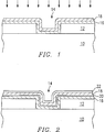
- Figure 1 is a cross sectional view of the fabrication of a semiconductor integrated circuit according to the present invention.
- Figure 2 is a cross sectional view of the fabrication of a alternative fabrication method of a semiconductor integrated circuit according to the present invention.
- an integrated circuit is to be formed on a silicon substrate 10.
- An interlevel dielectric layer 12 is formed by conventional methods over the substrate 10.
- An opening 14 is formed in the dielectric layer 12 to expose a portion of the substrate 10.
- a barrier layer 16 may be formed over the dielectric layer 12 and in the opening 14.
- Layer 16 will typically be a refractory metal such as titanium or tungsten or a refractory metal silicide.
- An aluminum layer 18 is formed over the barrier layer 16 and in the opening 14.
- the aluminum layer 18 is formed by chemical vapor deposition (CVD) techniques and preferably by low pressure CVD (LPCVD) to obtain a near conformal layer over the integrated circuit.
- CVD chemical vapor deposition
- LPCVD low pressure CVD
- the LPCVD aluminum deposition techniques will increase step coverage and provide a more conformal layer into interconnect openings.
- Silicon is then implanted into the aluminum to achieve a desired silicon concentration.
- An example of an implanted dosage is 6 X 10¹⁶ atoms/cm2 implanted into approximately 10,000 angstroms of aluminum to achieve approximately a one percent by weight silicon concentration in the aluminum.
- the appropriate concentration of silicon in the aluminum to create an aluminum-silicon alloy will prevent any substantial amount of silicon from the substrate from dissolving into the aluminum layer.
- FIG. 2 an alternative method of forming the aluminum-silicon alloy is shown.
- the process steps of forming the interlevel dielectric layer 12, the opening 14 and barrier layer 16, if formed, are the same as described above.
- a silicon layer 20 is deposited over the barrier layer 16 and in the opening 14.
- a substantially conformal aluminum layer 18 is then formed by LPCVD techniques over the silicon layer 20.
- the silicon layer 20 will dissolve into the aluminum layer 18.
- a silicon layer 22 may be formed over the conformal aluminum layer 18 after the aluminum layer is formed. Again, during subsequent processing steps, the silicon layer 22 will dissolve into the aluminum layer 18.
- the silicon layers 20 and 22 may be formed by sputter deposition techniques or by plasma enhanced chemical vapor deposition techniques to a desired thickness to form the necessary aluminum-silicon alloy. For example, approximately 120 angstroms of silicon will produce approximately a one percent by weight silicon concentration in approximately 10,000 angstroms of aluminum.
- silicon must still be used as a dopant in the aluminum films to prevent the silicon in the substrate from migrating across the barrier into the aluminum during subsequent processing steps.
- the invention described above may also be used between aluminum and polysilicon upper layers such as those used for signal lines and other contact vias. Using the silicon as a dopant in the aluminum will thus prevent junction spiking by providing a silicon concentration substantially equal to the solubility coefficient of the silicon in aluminum at any given temperature during subsequent processing steps.
- Aluminum-silicon alloys are currently used in todays technology typically by sputter deposition of both the aluminum and silicon.
- the primary advantage of the present invention is the formation of the aluminum by LPCVD techniques to provide a more conformal layer while still providing an aluminum-silicon alloy having the necessary concentration of silicon in the aluminum.
Landscapes
- Internal Circuitry In Semiconductor Integrated Circuit Devices (AREA)
Applications Claiming Priority (2)
| Application Number | Priority Date | Filing Date | Title |
|---|---|---|---|
| US89092092A | 1992-05-29 | 1992-05-29 | |
| US890920 | 1992-05-29 |
Publications (2)
| Publication Number | Publication Date |
|---|---|
| EP0572212A2 true EP0572212A2 (fr) | 1993-12-01 |
| EP0572212A3 EP0572212A3 (en) | 1994-05-11 |
Family
ID=25397337
Family Applications (1)
| Application Number | Title | Priority Date | Filing Date |
|---|---|---|---|
| EP19930304035 Withdrawn EP0572212A3 (en) | 1992-05-29 | 1993-05-25 | Method to form silicon doped cvd aluminium |
Country Status (2)
| Country | Link |
|---|---|
| EP (1) | EP0572212A3 (fr) |
| JP (1) | JPH06177061A (fr) |
Family Cites Families (4)
| Publication number | Priority date | Publication date | Assignee | Title |
|---|---|---|---|---|
| US3740835A (en) * | 1970-08-31 | 1973-06-26 | Fairchild Camera Instr Co | Method of forming semiconductor device contacts |
| US3881971A (en) * | 1972-11-29 | 1975-05-06 | Ibm | Method for fabricating aluminum interconnection metallurgy system for silicon devices |
| EP0420597B1 (fr) * | 1989-09-26 | 1996-04-24 | Canon Kabushiki Kaisha | Procédé pour la formation d'un film déposé en utilisant de l'alkyle de l'hydrure d'aluminium et procédé de fabrication d'un dispositif semi-conducteur |
| DE69127347T2 (de) * | 1990-11-29 | 1998-02-05 | At & T Corp | Verfahren zur Herstellung eines Kontakts für integrierte Schaltungen |
-
1993
- 1993-05-25 EP EP19930304035 patent/EP0572212A3/en not_active Withdrawn
- 1993-05-31 JP JP5128575A patent/JPH06177061A/ja active Pending
Also Published As
| Publication number | Publication date |
|---|---|
| EP0572212A3 (en) | 1994-05-11 |
| JPH06177061A (ja) | 1994-06-24 |
Similar Documents
| Publication | Publication Date | Title |
|---|---|---|
| US5527739A (en) | Process for fabricating a semiconductor device having an improved metal interconnect structure | |
| US8456007B2 (en) | Chemical vapor deposition of titanium | |
| US5420072A (en) | Method for forming a conductive interconnect in an integrated circuit | |
| EP0506129B1 (fr) | Procédé de formation d'un contact électrique à travers une couche isolante sur une pastille semi-conductrice | |
| EP0261846B1 (fr) | Méthode pour former, sur la surface d'un dispositif semi-conducteur, une couche métallique contenant du cuivre | |
| US6133147A (en) | Process for selective metal deposition in holes of semiconductor device | |
| US4732801A (en) | Graded oxide/nitride via structure and method of fabrication therefor | |
| US20020090796A1 (en) | Silicon layer to improve plug filling by CVD | |
| US5429989A (en) | Process for fabricating a metallization structure in a semiconductor device | |
| US6054382A (en) | Method of improving texture of metal films in semiconductor integrated circuits | |
| Gardner et al. | Layered and homogeneous films of aluminum and aluminum/silicon with titanium and tungsten for multilevel interconnects | |
| US5880023A (en) | Process for formation of wiring layer in semiconductor device | |
| US5874360A (en) | Manufacture of semiconductor devices | |
| US5795796A (en) | Method of fabricating metal line structure | |
| US6218295B1 (en) | Semiconductor structure with a titanium aluminum nitride layer and method for fabricating the same | |
| EP0298155B1 (fr) | Procédé pour former une couche de métal réfractaire | |
| EP0162950B1 (fr) | Procédé pour diffuser dans un substrat semi-conducteur une impureté déterminant la conductivité et pour réaliser un contact électrique avec celui-ci | |
| US6433434B1 (en) | Apparatus having a titanium alloy layer | |
| EP0572212A2 (fr) | Procédé de dépôt d'aluminium dopé au silicium par la méthode de dépôt chimique en phase vapeur | |
| US7943505B2 (en) | Advanced VLSI metallization | |
| US5569628A (en) | Semiconductor device fabrication method | |
| US6624073B2 (en) | Optimized TaCN thin film diffusion barrier for copper metallization | |
| JP3149912B2 (ja) | 半導体装置およびその製造方法 | |
| JP3288010B2 (ja) | 半導体素子の金属配線形成方法 | |
| US4992152A (en) | Reducing hillocking in aluminum layers formed on substrates |
Legal Events
| Date | Code | Title | Description |
|---|---|---|---|
| PUAI | Public reference made under article 153(3) epc to a published international application that has entered the european phase |
Free format text: ORIGINAL CODE: 0009012 |
|
| AK | Designated contracting states |
Kind code of ref document: A2 Designated state(s): DE FR GB IT |
|
| PUAL | Search report despatched |
Free format text: ORIGINAL CODE: 0009013 |
|
| AK | Designated contracting states |
Kind code of ref document: A3 Designated state(s): DE FR GB IT |
|
| 17P | Request for examination filed |
Effective date: 19941109 |
|
| STAA | Information on the status of an ep patent application or granted ep patent |
Free format text: STATUS: THE APPLICATION HAS BEEN WITHDRAWN |
|
| 18W | Application withdrawn |
Withdrawal date: 19970129 |