EP0572755B1 - Commande de mise en circuit pour dispositifs électriques - Google Patents
Commande de mise en circuit pour dispositifs électriques Download PDFInfo
- Publication number
- EP0572755B1 EP0572755B1 EP92830281A EP92830281A EP0572755B1 EP 0572755 B1 EP0572755 B1 EP 0572755B1 EP 92830281 A EP92830281 A EP 92830281A EP 92830281 A EP92830281 A EP 92830281A EP 0572755 B1 EP0572755 B1 EP 0572755B1
- Authority
- EP
- European Patent Office
- Prior art keywords
- circuit
- output
- input
- enabling
- turn
- Prior art date
- Legal status (The legal status is an assumption and is not a legal conclusion. Google has not performed a legal analysis and makes no representation as to the accuracy of the status listed.)
- Expired - Lifetime
Links
Images
Classifications
-
- H—ELECTRICITY
- H02—GENERATION; CONVERSION OR DISTRIBUTION OF ELECTRIC POWER
- H02H—EMERGENCY PROTECTIVE CIRCUIT ARRANGEMENTS
- H02H11/00—Emergency protective circuit arrangements for preventing the switching-on in case an undesired electric working condition might result
-
- H—ELECTRICITY
- H03—ELECTRONIC CIRCUITRY
- H03F—AMPLIFIERS
- H03F1/00—Details of amplifiers with only discharge tubes, only semiconductor devices or only unspecified devices as amplifying elements
- H03F1/30—Modifications of amplifiers to reduce influence of variations of temperature or supply voltage or other physical parameters
- H03F1/305—Modifications of amplifiers to reduce influence of variations of temperature or supply voltage or other physical parameters in case of switching on or off of a power supply
Definitions
- the present invention relates to a turn-on control circuit for devices, in particular power devices, having a circuit for detecting error, fault or otherwise undesired conditions.
- the present invention is particularly suitable for devices, such as described in EP-A-0 368 528, having an input supplied with an electric quantity, which, when the device is turned on, switches gradually from a first to a second steady-state value, such as those with a standby input (to which the following description refers purely by way of example), which are designed to switch from a standby state wherein the voltage at the standby input is low, to an operating (play) state.
- Typical devices of this sort are audio amplifiers to which the following description refers.
- errors or faults may occur at times in the connections between the amplifier outputs and the load (loudspeakers).
- the output may be grounded or connected to the supply line due to an insulation fault in the cable supplying the signal to the load; the load may be disconnected due to an interruption in the signal supply cable; or metal fragments on the printed circuit on which the connections are made may result in shortcircuiting of the outputs or of points of different potential.
- a clamping element connected to the input of the circuit is activated for preventing any further increase in input voltage and so preventing the device from being turned on.
- the system according to the present invention is particularly suitable for amplifiers connected permanently to the supply, such as those with a standby input compatible with CMOS logic levels.
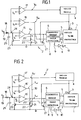
- Number 1 in Fig.1 indicates the device to be protected (in this case, an audio amplifier), and number 2 the turn-on control circuit.
- Device 1 presents an enabling input 3 (EN) connected to the output of a DEVICE ENABLING block 4 containing all the voltage and current sources necessary for operation of device 1; an input 5 connected to the output of a DIAGNOSTIC ENABLING block 6 containing all the voltage and current sources required for pre-turn-on diagnosis; and an output 7 (of n lines) connected to the input of a FAULT DETECTING block 8 for detecting any undesired conditions which may result in faulty operation of device 1.
- EN enabling input 3
- DEVICE ENABLING block 4 containing all the voltage and current sources necessary for operation of device 1
- an input 5 connected to the output of a DIAGNOSTIC ENABLING block 6 containing all the voltage and current sources required for pre-turn-on diagnosis
- an output 7 (of n lines) connected to the input of a FAULT DETECTING block
- Fault detecting block 8 (which, together with diagnostic enabling block 6, forms a fault detecting stage) presents an output 9 to which any information relative to the presence of undesired conditions is supplied, and which is connected to a number m of lines 10 (one for each possible malfunctioning condition) having a buffer circuit 11.
- Circuit 2 also comprises three comparators 15, 16, 17 having their positive inputs connected (via resistor 18) to a standby input 19 supplied with standby voltage V ST , and their negative inputs connected to respective reference potentials V1, V2, V3, where V1 ⁇ V2 ⁇ V3.
- the output of comparator 15 (potential V o1 ) is connected to the enabling input of diagnostic enabling block 6 and to one terminal of a controlled switch 20, the control terminal of which is connected to one output of fault detecting block 8, and the other terminal of which is connected via resistor 21 to the collector of an NPN type transistor 22 (defining a disabling element) having its base connected to the output of comparator 16 (potential V o2 ) and its emitter grounded (reference potential).
- the collector of transistor 22 is also connected to the base of a second NPN type transistor 23 (defining a clamping element) having its emitter grounded and its collector connected to the common node 24 of the positive inputs of comparators 15-17. Between node 24 and ground, provision is made for a capacitor 25 defining a low-pass filter with resistor 18.
- comparator 17 (potential V o3 ) is connected to the enabling input of device enabling block 4; and a third NPN type transistor 27 (defining a diagnostic disabling element) presents its collector connected to the output of comparator 15, its base connected to the output of device enabling block 4, and its emitter grounded.
- control circuit 2 is preferably integrated on the same chip as device 1.
- the Fig.1 circuit operates as follows.
- V ST In the absence of undesired conditions ("faults"), the increase in V ST presents the following phases: 1) V ST ⁇ V 1
- output potential V o1 of comparator 15 is high, thus enabling diagnostic enabling block 6, for determining the presence of any error conditions; V o2 is low, so that transistor 22 remains off; and V o3 is also low, so that device enabling block 4 is disabled and device 1 remains off.
- comparator 17 switches so as to enable device enabling block 4 and turn on the sources of device 1 and, consequently, device 1 itself.
- block 4 also turns on transistor 27, which grounds the output of comparator 15, thus disabling the diagnostic system (blocks 6, 8), so that device 1 operates normally.
- Fig.2 shows a variation 2' of circuit 2 in Fig.1.
- Circuit 2' is similar to that of Fig.1, and again comprises three comparators 15', 16', 17' supplying respective output potentials V o1' , V o2' , V o3' ; blocks 4, 6, 8; transistors 22, 23, 27; switch 20; and capacitor 25.
- the only difference as compared with circuit 2 lies in the connection of the outputs of comparators 16' and 17' to switch 20 and transistor 22, and more specifically in the fact that, instead of controlling the base of transistor 21, the output of comparator 16' is connected to one terminal of switch 20 (the other terminal of which is again connected to resistor 21); while the base of transistor 22 is connected directly to the output of comparator 17' over line 30.
- comparator 15' in circuit 2' provides for enabling the diagnostic functions by enabling block 6 as soon as voltage V ST exceeds V1. In the event of a fault being detected by block 8, this closes switch 20 while still allowing voltage V ST to reach V2 by virtue of the fact that, previous to V2, the output of comparator 16' is still low, and transistor 23 remains off. Conversely, in the event of a fault being detected, as soon as V ST ⁇ V2, the output of comparator 16' switches to high, thus turning on transistor 23 and preventing any further increase in V ST as long as the fault persists; and switch 20 is maintained closed by the output of fault detecting block 8.
- the Fig.2 variation is ideal in situations in which the enabling phase of diagnostic enabling block 6 may result in spurious output signals being supplied to fault detecting block 8, thus turning on transistor 23 and so preventing device 1 from being turned on even in the absence of a fault at outputs 7. This possibility is prevented by circuit 2' by virtue of V ST only being clamped when V ST > V2, i.e. when diagnostic enabling block 6 is fully operative and therefore no longer in any condition to produce spurious output signals.
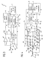
- Fig.3 shows a further variation 2" of the turn-on control circuit similar to that of Fig.1 and comprising blocks 4, 6, 8 and transistors 22, 23, 27.
- two comparators 15" and 17" having the negative inputs connected to respective threshold potentials V1 and V3, and supplying respective output potentials V o1'' and V o3'' ; the terminal of switch 20 not connected to resistor 21 is connected directly to the output of comparator 15''; and the base of transistor 22 is connected directly to the output of comparator 17'' over line 30.
- the remainder of circuit 2'' is identical to that of Fig.s 1 and 2.
- Circuit 2'' is thus extremely straightforward in design, and suitable for situations in which no danger exists of spurious signals being supplied when diagnostic enabling block 4 is turned on or during the final phase in the increase of input voltage V ST .
- Fig.4 shows a circuit diagram implementing the Fig.1 block diagram.
- Fig.4 shows resistor 18 between input 19 and node 24; capacitor 25 between node 24 and ground; and transistor 23 having the collector connected to node 24, the emitter grounded, and the base connected via resistor 21 to the output of a range comparator 40 implementing fault detecting block 8 and switch 20.
- Range comparator 40 presents two inputs 41, 42 set to respective threshold potentials V4, V5, where V4 ⁇ V5; and a third input connected to output 7 of device 1.
- output 7 coincides with input 5 of device 1, and is connected to the output of diagnostic enabling block 6 via a resistor 43.
- Block 6 implements, among other things, a reference voltage source, wherein V REF ⁇ V CC .
- the Fig.4 circuit also comprises a band-gap voltage source stage 44 including a pair of NPN type transistors 45, 46 having respective emitter areas A1 and A2, where A1 > A2.
- the base terminals of transistors 45, 46 are connected to each other and to node 24; the emitter terminal of transistor 46 is grounded via resistor 47; the emitter terminal of transistor 45 is connected to that of transistor 46 via a second resistor 48 (of resistance R1); the collector terminal of transistor 45 is connected to the cathode of a diode 49 having its anode connected to a supply line 50 set to potential V CC ; and the collector terminal of transistor 46 is connected to that of a PNP type transistor 51 having its emitter connected to line 50, and its base connected to the cathode of diode 49.
- the collector terminal of transistor 51 is also connected to the base terminal of a diode-connected PNP type transistor 53 having its collector shortcircuited to the base, and its emitter terminal connected to line 50.
- the collector terminal of transistor 51 is also connected to the base terminals of three PNP type transistors 54, 55, 56, each forming a respective current mirror circuit with transistor 53.
- Transistors 54, 55 and 56 present emitter terminals connected to line 50, and collector terminals connected to the base terminals of respective NPN type transistors 58, 59, 60, the emitter terminals of which are grounded.
- respective resistors 61, 62, 63 having respective resistances R2, R3, R4, where R2 > R3 > R4.
- the collector terminal of transistor 58 (forming comparator 15 together with transistor 54 and resistor 61) is connected to the enabling input of diagnostic enabling block 6 and range comparator 40; the collector terminal of transistor 59 (forming comparator 16 together with transistor 55 and resistor 62) is connected to the input of a current mirror circuit 65 including a diode 66 (having its anode connected to line 50 and its cathode to the collector of transistor 59) and a PNP type transistor 67 (connected by the emitter terminal to line 50, by the base terminal to the cathode of diode 66, and by the collector terminal to the base terminal of transistor 22); and the collector terminal of transistor 60 (forming comparator 17 together with transistor 56 and resistor 63) is connected to the enabling input of device enabling block 4.
- a current mirror circuit 65 including a diode 66 (having its anode connected to line 50 and its cathode to the collector of transistor 59) and a PNP type transistor 67 (connected by the emitter terminal to line 50,
- the Fig.4 circuit operates as follows.
- diode 53 is supplied with current equal to the difference between the currents in components 49 and 51 (collector currents of transistors 45 and 46) which in turn are related in known manner to input voltage V ST . Consequently, as input voltage V ST increases, the drive current of transistor 53 and thus current I through the transistor also increases, which current I is mirrored in transistors 54, 55 and 56 and supplied to resistors 61, 62 and 63, thus causing a voltage drop at the base-emitter junction of respective transistors 58-60. Transistors 58-60 are turned on as soon as the voltage drop at the respective base-emitter junction reaches roughly 0.7 V. Therefore, by virtue of R2 > R3 > R4, the increase in V ST first turns on transistor 58 followed by transistor 59 and, finally, transistor 60.
- transistor 58 As soon as it is turned on, transistor 58 generates a collector voltage V o1 capable of enabling the voltage source implemented by block 6 and range comparator 40, so that block 6 supplies reference output voltage V REF to terminal 5, 7 of device 1, which in this phase is in a tri-state condition. If terminal 5, 7 is is not grounded or switched to V CC , it therefore switches to V REF , so that comparator 40 presents a low output, transistor 23 remains off, and voltage V ST may continue rising until it reaches the value at which transistor 59 is turned on, thus turning on current mirror 65 and transistor 22, and preventing transistor 23 from being turned on even when, under normal operating conditions of device 1, the voltage at output 5, 7 exceeds V5 or falls below V4.
- transistor 60 is also turned on, which enables block 4 for turning on device 1. Though not shown, in this case also, the collector terminal of transistor 60 may obviously drive transistor 27 for disabling diagnostic enabling block 6.
- circuit according to the present invention provides for preventing the device from being turned on under potentially dangerous conditions, even if no other protection is provided for.
- the circuit may also be employed for supplying diagnostic signals to the user (person or control microprocessor) and so enabling any problems detected to be eliminated by the user. This is particularly useful when assembling the equipment featuring the controlled device (e.g. audio amplifier) for enabling any faulty connections to be detected and rectified prior to sale.
- the controlled device e.g. audio amplifier
- the circuit provides for supplying simple output information (e.g. the signal produced by one or more open-collector type outputs) or complex information (e.g. via a serial or parallel bus), and requires no particular processing speed on the part of the user, by virtue of the device remaining protected as long as the fault persists. Moreover, once the fault is rectified, the turn-on sequence continues automatically, with no need for restarting or resetting the turn-on voltage.
- simple output information e.g. the signal produced by one or more open-collector type outputs
- complex information e.g. via a serial or parallel bus
- the circuit according to the present invention is also compatible with any diagnostic system operating during normal operation of the amplifier, even using the same fault detecting block and the same output buffer.
- the diagnostic enabling and fault detecting blocks may be of different types; the device to be protected may be an audio amplifier, a less complex stage, or even a more complex unit; the circuit may be integrated with the device or formed separately; and, as opposed to the different sizing of resistors 61-63, transistors 58-60 in the Fig.4 circuit may be turned on sequentially by providing drive transistors 54-56 with different emitter area ratios so that they are turned on by different base currents.
Landscapes
- Engineering & Computer Science (AREA)
- Power Engineering (AREA)
- Amplifiers (AREA)
- Control Of Amplification And Gain Control (AREA)
- Protection Of Static Devices (AREA)
Claims (15)
- Circuit (2 ; 2' ; 2") pour la commande de mise en route d'un dispositif (1) nécessitant une protection contre des conditions indésirées, le dispositif (1) pouvant être connecté à une entrée de mise en route (19) alimentée par une quantité électrique de commande de mise en route (VST) dont la valeur varie pendant la mise en route, le dispositif (1) étant tel qu'il n'est pas mis en route tant que la quantité électrique (VST) n'a pas atteint une valeur prédéterminée (V₃), et également à un étage de détection de défauts (6, 8) pour produire un signal de défaut dans le cas où un état indésiré est détecté dans le dispositif (1), caractérisé en ce qu'il comprend un premier moyen de comparaison (15, 15', 15") ayant une entrée (24) pouvant être connectée à l'entrée de mise en route (19) et une sortie pouvant être connectée à l'étage de détection de défauts (6, 8), le premier moyen de comparaison produisant un signal (Vo1 ; Vo1' ; Vo1'') validant le fonctionnement de l'étage de détection de défauts (6, 8) quand la quantité électrique (VST) atteint une première valeur (V₁) ; un élément de verrouillage (23) ayant une borne de validation alimentée par un signal de validation de verrouillage, et une borne de verrouillage pouvant être connectée à ladite entrée (24) du premier moyen de comparaison pour empêcher la quantité électrique (VST) de varier et d'atteindre ladite valeur prédéterminée (V₃) en présence du signal de validation de verrouillage ; et des moyens de circuit (20, 21) pouvant être connectés à l'étage de détection de défauts (6, 8) et connectés à la borne de validation de l'élément de verrouillage (23), lesdits moyens de circuit produisant le signal de validation de verrouillage en présence du signal de défaut.
- Circuit (2 ; 2' ; 2'') pour la commande de mise en route d'un dispositif (1) nécessitant une protection contre des conditions indésirées, ce circuit comprenant une entrée de mise en route (19) alimentée par une quantité électrique de commande de mise en route (VST) dont la valeur varie pendant la mise en route, le dispositif (1) étant tel qu'il n'est pas mis en route tant que la quantité électrique (VST) n'a pas atteint une valeur prédéterminée (V₃) ; et un étage de détection de défauts (6, 8) pour produire un signal de défaut dans le cas où une condition indésirée est détectée dans le dispositif (1), caractérisé en ce qu'il comprend un premier moyen de comparaison (15 ; 15' ;15'') ayant une entrée (24) connectée à l'entrée de mise en route (19), et une sortie connectée à l'étage de détection de défauts (6, 8), le premier moyen de comparaison produisant un signal (VO1, VO1' ; VO1'') validant le fonctionnement de l'étage de détection de défauts (6, 8) quand la quantité électrique (VST) atteint une première valeur (V₁) ; un élément de verrouillage (23) ayant une borne de validation alimentée par un signal de validation de verrouillage, et une borne de verrouillage pouvant être connectée à l'entrée (24) du premier moyen de comparaison (15 ; 15' ; 15'') pour empêcher la quantité électrique (VST) de varier et d'atteindre la valeur prédéterminée (V₃) en présence du signal de validation de verrouillage ; et des moyens de circuit (20, 21) connectés à l'étage de détection de défauts et à ladite borne de validation de l'élément de verrouillage (23) pour produire le signal de validation de verrouillage en présence du signal de défaut.
- Circuit selon la revendication 1 ou 2, caractérisé en ce que la quantité électrique est une tension (VST) qui augmente progressivement pendant la mise en route.
- Circuit selon la revendication 3, caractérisé en ce qu'il comprend un moyen de comparaison (16 ; 16' ; 17'') ayant une entrée connectée à l'entrée de mise en route (19) et une sortie produisant un signal (VO2 ; VO2' ; VO3'') quand ladite tension (VST) présente une seconde valeur (V₂ ; V₃) supérieure à la première valeur (V1) en ce que les moyens de circuit (20, 21) sont connectés à la sortie (15, 15'' ; 16') de l'un du premier moyen de comparaison (15 ; 15' ; 15'') et du moyen de comparaison (16 ; 16' ; 17'') ; et en ce que l'élément de verrouillage (23) définit un trajet de contre-réaction entre l'entrée de mise en route (19) et la sortie de l'un (15 ; 15" ; 16') du premier moyen de comparaison (15 ; 15' ; 15'') et du moyen de comparaison (16, 16' ; 17'').
- Circuit selon la revendication 3 ou 4, caractérisé en ce que l'élément de verrouillage est un transistor (23) ayant une première borne connectée à l'entrée de mise en route (19), une deuxième borne connectée à une ligne de potentiel de référence telle que la masse, et une borne de commande connectée auxdits moyens de circuit (20, 21).
- Circuit selon l'une des revendications 3 à 5, caractérisé en ce que les moyens de circuit (20, 21) comprennent un commutateur (20) disposé entre la sortie du premier moyen de comparaison (15 ; 15") et la borne de validation de l'élément de verrouillage (23), et comprenant une borne de commande connectée à l'étage de détection de défauts (6, 8).
- Circuit selon la revendication 6, caractérisé en ce qu'il comprend un second moyen de comparaison (16, 17") ayant une entrée connectée à l'entrée de mise en route (19) et une sortie produisant un signal d'inhibition de verrouillage (VO2 ; VO3'') quand la tension (VST) atteint une seconde valeur (V₂ ; V₃) supérieure à la première valeur (V₁) ; et un élément d'inhibition (22) ayant une borne de commande connectée à la sortie du second moyen de comparaison (16 ; 17") et une borne connectée à la borne de validation de l'élément de verrouillage (23) pour produire un signal inhibant le signal de verrouillage en présence du signal d'inhibition de verrouillage (VO2 ; VO3'').
- Circuit selon la revendication 7, caractérisé en ce que l'élément d'inhibition comprend un transistor bipolaire (22) ayant sa borne de base connectée à la sortie du second moyen de comparaison (16 ; 17'').
- Circuit selon la revendication 7 ou 8, caractérisé en ce que la sortie du second moyen de comparaison (17") est également connectée à un étage (4) de validation du dispositif ayant une sortie connectée audit dispositif (1).
- Circuit selon la revendication 7 ou 8, caractérisé en ce qu'il comprend un troisième moyen de comparaison (17) ayant une entrée connectée à l'entrée de mise en route (19) et une sortie, et produisant un signal (VO3) de validation du dispositif quand ladite tension (VST) présente une troisième valeur (V₃) supérieure à la deuxième valeur (V₂) ; et en ce qu'il comprend un étage (4) de validation du dispositif ayant une entrée connectée à la sortie du troisième moyen de comparaison (17) et une sortie connectée audit dispositif (1).
- Circuit selon la revendication 9 ou 10, caractérisé en ce qu'il comprend un élément d'inhibition de diagnostic (27) connecté à l'étage de détection de défauts (6, 8) et ayant une borne de commande connectée à la sortie de l'étage (4) de validation du dispositif.
- Circuit selon la revendication 11, caractérisé en ce que l'élément d'inhibition de diagnostic comprend un transistor (27) ayant des première et seconde bornes connectées à l'étage de détection de défauts (6, 8) et à une ligne de potentiel de référence telle que la masse.
- Circuit selon l'une des revendications 3 à 5, caractérisé en ce qu'il comprend un second moyen de comparaison (16') ayant une entrée connectée à l'entrée de mise en route (19) et une sortie connectée auxdits moyens de circuit (20, 21) pour produire un signal de validation de verrouillage (VO2') quand la tension (VST) présente une seconde valeur (V₂) supérieure à la première valeur (V₁) ; un troisième moyen de comparaison (17') ayant une entrée connectée à l'entrée de mise en route et une sortie connectée à un étage (4) de validation du dispositif, pour produire un signal (VO3') d'inhibition de verrouillage quand la tension d'entrée présente une troisième valeur (V₃) supérieure à la deuxième valeur ; un élément d'inhibition (22) ayant une borne de commande connectée à la sortie du troisième moyen de comparaison (17') et une borne d'inhibition connectée à la borne de validation de l'élément de verrouillage (23), pour produire un signal inhibant l'élément de verrouillage en présence du signal d'inhibition de verrouillage (vO3') ; et en ce que les moyens de circuit (20, 21) comprennent un commutateur (20) disposé entre la sortie du second moyen de comparaison (16') et la borne de validation de l'élément de verrouillage (23) et ayant une borne de commande connectée à l'étage de détection de défauts (6, 8).
- Circuit selon la revendication 13, caractérisé en ce qu'il comprend un transistor d'inhibition de diagnostic (27) ayant des première et seconde bornes connectées à l'étage de détection de défauts (6, 8) et à une ligne de potentiel de référence telle que la masse, et une borne de commande connectée à la sortie de l'étage (4) de validation du dispositif.
- Circuit selon l'une quelconque des revendications 1 à 14, caractérisé en ce qu'il comprend un circuit de source de courant commandée (44) ayant une entrée de commande connectée à l'entrée de mise en route (19) et une sortie, et produisant un courant corrélé à ladite tension (VST) ; un circuit de miroir de courant (53, 54) ayant une entrée connectée à la sortie du circuit de source de courant (44) et une sortie ; et un élément de transistor (58) ayant une première borne définissant ladite sortie du premier moyen de comparaison (15), une seconde borne connectée à une ligne de potentiel de référence telle que la masse, et une borne de commande connectée à la sortie du circuit de miroir de courant, un élément résistif (61) étant prévu entre la borne de commande de l'élément de transistor (58) et la ligne de potentiel de référence.
Priority Applications (4)
| Application Number | Priority Date | Filing Date | Title |
|---|---|---|---|
| DE69209058T DE69209058T2 (de) | 1992-05-29 | 1992-05-29 | Einschaltungssteuerung für elektrische Geräte |
| EP92830281A EP0572755B1 (fr) | 1992-05-29 | 1992-05-29 | Commande de mise en circuit pour dispositifs électriques |
| US08/069,283 US5535082A (en) | 1992-05-29 | 1993-05-28 | Turn-on control circuit for electric devices |
| JP12935993A JP3384834B2 (ja) | 1992-05-29 | 1993-05-31 | ターンオン制御回路 |
Applications Claiming Priority (1)
| Application Number | Priority Date | Filing Date | Title |
|---|---|---|---|
| EP92830281A EP0572755B1 (fr) | 1992-05-29 | 1992-05-29 | Commande de mise en circuit pour dispositifs électriques |
Publications (2)
| Publication Number | Publication Date |
|---|---|
| EP0572755A1 EP0572755A1 (fr) | 1993-12-08 |
| EP0572755B1 true EP0572755B1 (fr) | 1996-03-13 |
Family
ID=8212117
Family Applications (1)
| Application Number | Title | Priority Date | Filing Date |
|---|---|---|---|
| EP92830281A Expired - Lifetime EP0572755B1 (fr) | 1992-05-29 | 1992-05-29 | Commande de mise en circuit pour dispositifs électriques |
Country Status (4)
| Country | Link |
|---|---|
| US (1) | US5535082A (fr) |
| EP (1) | EP0572755B1 (fr) |
| JP (1) | JP3384834B2 (fr) |
| DE (1) | DE69209058T2 (fr) |
Families Citing this family (10)
| Publication number | Priority date | Publication date | Assignee | Title |
|---|---|---|---|---|
| DE69320974T2 (de) * | 1993-12-31 | 1999-02-04 | Stmicroelectronics S.R.L., Agrate Brianza, Mailand/Milano | Operationsverstärkerschutzschaltkreis, der entweder im Betrieb oder beim Einschalten die gleichen Schaltkreiselemente zur Erkennung von permanenten anormalen Ausgangszuständen benutzt |
| FR2765342B1 (fr) * | 1997-06-26 | 1999-07-30 | Commissariat Energie Atomique | Procede et dispositif de gestion du fonctionnement sous irradiation d'un composant electronique a transistors mos complementaires |
| JP3528557B2 (ja) * | 1997-12-22 | 2004-05-17 | トヨタ自動車株式会社 | 燃焼式ヒータを有する内燃機関 |
| JP4058767B2 (ja) * | 2004-11-04 | 2008-03-12 | 船井電機株式会社 | スイッチング電源装置 |
| JP4936698B2 (ja) * | 2005-09-22 | 2012-05-23 | 株式会社東芝 | パワーアンプシステム |
| KR100833706B1 (ko) | 2007-02-01 | 2008-05-29 | 삼성전자주식회사 | 감광성 폴리이미드 조성물, 폴리이미드 필름 및 이를 이용한 반도체 소자 |
| US10061330B2 (en) * | 2011-12-21 | 2018-08-28 | Lennox Industries Inc. | HVAC system having a diagnostics controller associated therewith |
| US20200264229A1 (en) * | 2019-02-15 | 2020-08-20 | Qualcomm Incorporated | Soc imminent failure prediction using aging sensors |
| CN111585516B (zh) * | 2020-06-15 | 2023-03-03 | 电子科技大学 | 一种带输出箝位功能的运算放大器 |
| CN115275959B (zh) * | 2022-07-20 | 2026-04-07 | 珠海格力电器股份有限公司 | 一种电源输入防反接电路、电源模块以及用电设备 |
Family Cites Families (6)
| Publication number | Priority date | Publication date | Assignee | Title |
|---|---|---|---|---|
| US4146847A (en) * | 1976-11-05 | 1979-03-27 | Trio Kabushiki Kaisha | Power limiting circuitry for use with power amplifier |
| US4517618A (en) * | 1983-09-06 | 1985-05-14 | The United States Of America As Represented By The Secretary Of The Air Force | Protection circuitry for high voltage drivers |
| IT1213158B (it) * | 1984-04-20 | 1989-12-14 | Ates Componenti Elettron | Circuito di controllo dell'accensione per amplificatore audio. |
| DE3428441A1 (de) * | 1984-08-01 | 1986-02-13 | Siemens AG, 1000 Berlin und 8000 München | Schalteinrichtung fuer die stromzufuhr an ein elektrisches geraet |
| IT1229860B (it) * | 1988-11-09 | 1991-09-13 | Sgs Thomson Microelectronics | Amplificatore audio integrato con regolazione unificata delle funzioni di "mute" e "stand by" e dei transitori di commutazione. |
| US5202590A (en) * | 1991-11-06 | 1993-04-13 | Intel Corporation | Subthreshold sense circuit for clamping an injected current |
-
1992
- 1992-05-29 EP EP92830281A patent/EP0572755B1/fr not_active Expired - Lifetime
- 1992-05-29 DE DE69209058T patent/DE69209058T2/de not_active Expired - Fee Related
-
1993
- 1993-05-28 US US08/069,283 patent/US5535082A/en not_active Expired - Lifetime
- 1993-05-31 JP JP12935993A patent/JP3384834B2/ja not_active Expired - Fee Related
Also Published As
| Publication number | Publication date |
|---|---|
| US5535082A (en) | 1996-07-09 |
| JPH0637550A (ja) | 1994-02-10 |
| EP0572755A1 (fr) | 1993-12-08 |
| DE69209058D1 (de) | 1996-04-18 |
| JP3384834B2 (ja) | 2003-03-10 |
| DE69209058T2 (de) | 1996-10-24 |
Similar Documents
| Publication | Publication Date | Title |
|---|---|---|
| US5596465A (en) | Overcurrent protection circuit for a dc-to-dc converter | |
| US5623254A (en) | Drive circuit fault detection drive | |
| EP0580923A1 (fr) | Circuit pour la détection de variations de tension en relation avec une tension de référence pour dispositifs comprenant des amplifications d'erreurs | |
| JP4296811B2 (ja) | 物理量センサ装置 | |
| EP0572755B1 (fr) | Commande de mise en circuit pour dispositifs électriques | |
| US5224169A (en) | Protection arrangement for an audio output channel | |
| US5896263A (en) | Output circuit having electronic overload protection activated by voltage drop across output transistor | |
| US4481553A (en) | Protection circuit | |
| CA2075555A1 (fr) | Protection des dispositifs a semiconducteur contre les transitoires de grande energie | |
| US6292341B1 (en) | Bidirectional electronic switch | |
| US5432945A (en) | Output control and protection device, in particular for programmable automatic controllers | |
| US3860855A (en) | Multiple voltage source imbalance detection and protection circuit | |
| JP2682699B2 (ja) | 駆動回路 | |
| US4445160A (en) | Fault-powered low-level voltage clamp circuit | |
| JP2020167860A (ja) | 処理回路および電源装置 | |
| JPH06222099A (ja) | 負荷異常状態検知回路 | |
| JP3267108B2 (ja) | モータの制御装置 | |
| JP3425004B2 (ja) | 地絡電流検出装置 | |
| KR900009468Y1 (ko) | 과부하시 전원 차단회로 | |
| JP2963287B2 (ja) | 半導体集積回路装置 | |
| KR0164349B1 (ko) | 디지탈 교환시스템의 u인터페이스 전원공급 제어회로 | |
| JP3664038B2 (ja) | リセット回路 | |
| JPH0453335B2 (fr) | ||
| JPH0628912Y2 (ja) | 過電圧保護回路 | |
| JP2002010472A (ja) | 過電流保護回路及びそれを内蔵した電気機器 |
Legal Events
| Date | Code | Title | Description |
|---|---|---|---|
| PUAI | Public reference made under article 153(3) epc to a published international application that has entered the european phase |
Free format text: ORIGINAL CODE: 0009012 |
|
| 17P | Request for examination filed |
Effective date: 19930331 |
|
| AK | Designated contracting states |
Kind code of ref document: A1 Designated state(s): DE FR GB IT NL PT |
|
| 17Q | First examination report despatched |
Effective date: 19950519 |
|
| GRAH | Despatch of communication of intention to grant a patent |
Free format text: ORIGINAL CODE: EPIDOS IGRA |
|
| GRAA | (expected) grant |
Free format text: ORIGINAL CODE: 0009210 |
|
| AK | Designated contracting states |
Kind code of ref document: B1 Designated state(s): DE FR GB IT NL PT |
|
| PG25 | Lapsed in a contracting state [announced via postgrant information from national office to epo] |
Ref country code: NL Free format text: LAPSE BECAUSE OF FAILURE TO SUBMIT A TRANSLATION OF THE DESCRIPTION OR TO PAY THE FEE WITHIN THE PRESCRIBED TIME-LIMIT Effective date: 19960313 |
|
| ITF | It: translation for a ep patent filed | ||
| REF | Corresponds to: |
Ref document number: 69209058 Country of ref document: DE Date of ref document: 19960418 |
|
| PG25 | Lapsed in a contracting state [announced via postgrant information from national office to epo] |
Ref country code: PT Effective date: 19960614 |
|
| ET | Fr: translation filed | ||
| NLV1 | Nl: lapsed or annulled due to failure to fulfill the requirements of art. 29p and 29m of the patents act | ||
| PLBE | No opposition filed within time limit |
Free format text: ORIGINAL CODE: 0009261 |
|
| 26N | No opposition filed | ||
| REG | Reference to a national code |
Ref country code: GB Ref legal event code: IF02 |
|
| PGFP | Annual fee paid to national office [announced via postgrant information from national office to epo] |
Ref country code: DE Payment date: 20020610 Year of fee payment: 11 |
|
| PG25 | Lapsed in a contracting state [announced via postgrant information from national office to epo] |
Ref country code: DE Free format text: LAPSE BECAUSE OF NON-PAYMENT OF DUE FEES Effective date: 20031202 |
|
| PGFP | Annual fee paid to national office [announced via postgrant information from national office to epo] |
Ref country code: FR Payment date: 20040510 Year of fee payment: 13 |
|
| PGFP | Annual fee paid to national office [announced via postgrant information from national office to epo] |
Ref country code: GB Payment date: 20040526 Year of fee payment: 13 |
|
| PG25 | Lapsed in a contracting state [announced via postgrant information from national office to epo] |
Ref country code: IT Free format text: LAPSE BECAUSE OF NON-PAYMENT OF DUE FEES;WARNING: LAPSES OF ITALIAN PATENTS WITH EFFECTIVE DATE BEFORE 2007 MAY HAVE OCCURRED AT ANY TIME BEFORE 2007. THE CORRECT EFFECTIVE DATE MAY BE DIFFERENT FROM THE ONE RECORDED. Effective date: 20050529 Ref country code: GB Free format text: LAPSE BECAUSE OF NON-PAYMENT OF DUE FEES Effective date: 20050529 |
|
| GBPC | Gb: european patent ceased through non-payment of renewal fee |
Effective date: 20050529 |
|
| PG25 | Lapsed in a contracting state [announced via postgrant information from national office to epo] |
Ref country code: FR Free format text: LAPSE BECAUSE OF NON-PAYMENT OF DUE FEES Effective date: 20060131 |
|
| REG | Reference to a national code |
Ref country code: FR Ref legal event code: ST Effective date: 20060131 |