EP0572847A1 - Détecteur de pièces de monnaie - Google Patents
Détecteur de pièces de monnaie Download PDFInfo
- Publication number
- EP0572847A1 EP0572847A1 EP93107938A EP93107938A EP0572847A1 EP 0572847 A1 EP0572847 A1 EP 0572847A1 EP 93107938 A EP93107938 A EP 93107938A EP 93107938 A EP93107938 A EP 93107938A EP 0572847 A1 EP0572847 A1 EP 0572847A1
- Authority
- EP
- European Patent Office
- Prior art keywords
- coin
- coil
- circuit
- oscillator
- conductor
- Prior art date
- Legal status (The legal status is an assumption and is not a legal conclusion. Google has not performed a legal analysis and makes no representation as to the accuracy of the status listed.)
- Granted
Links
Images
Classifications
-
- G—PHYSICS
- G07—CHECKING-DEVICES
- G07D—HANDLING OF COINS OR VALUABLE PAPERS, e.g. TESTING, SORTING BY DENOMINATIONS, COUNTING, DISPENSING, CHANGING OR DEPOSITING
- G07D5/00—Testing specially adapted to determine the identity or genuineness of coins, e.g. for segregating coins which are unacceptable or alien to a currency
- G07D5/08—Testing the magnetic or electric properties
-
- G—PHYSICS
- G07—CHECKING-DEVICES
- G07D—HANDLING OF COINS OR VALUABLE PAPERS, e.g. TESTING, SORTING BY DENOMINATIONS, COUNTING, DISPENSING, CHANGING OR DEPOSITING
- G07D5/00—Testing specially adapted to determine the identity or genuineness of coins, e.g. for segregating coins which are unacceptable or alien to a currency
- G07D5/02—Testing the dimensions, e.g. thickness, diameter; Testing the deformation
-
- Y—GENERAL TAGGING OF NEW TECHNOLOGICAL DEVELOPMENTS; GENERAL TAGGING OF CROSS-SECTIONAL TECHNOLOGIES SPANNING OVER SEVERAL SECTIONS OF THE IPC; TECHNICAL SUBJECTS COVERED BY FORMER USPC CROSS-REFERENCE ART COLLECTIONS [XRACs] AND DIGESTS
- Y10—TECHNICAL SUBJECTS COVERED BY FORMER USPC
- Y10T—TECHNICAL SUBJECTS COVERED BY FORMER US CLASSIFICATION
- Y10T29/00—Metal working
- Y10T29/49—Method of mechanical manufacture
- Y10T29/49002—Electrical device making
- Y10T29/4902—Electromagnet, transformer or inductor
Definitions
- the invention relates to an inductive coin detector and a method for its production of the type mentioned in the preamble of claim 1.
- Such inductive coin detectors are suitable, for example, for the identification of coins in coin validators.
- An inductive coin detector of the type mentioned in the preamble of claim 1 is known from GB-A 2'151'062.
- the coin detector consists of a flat coil in the circuit of a high-frequency oscillator.
- An alternating magnetic field emerging from the coil perpendicularly penetrates a coin channel.
- a coin rolling through the alternating field in the coin channel changes the resonance frequency of the oscillator through the interaction of the coin with the alternating field.
- the frequency deviation caused by the presence of the coin serves as a measure of the parameter to be measured, such as. B. diameter, alloy, presence in general etc.
- the coil is wound from wire or made on a printed circuit board by etching a lamination of copper.
- the rest of the high-frequency oscillator, which is situated further away, is connected to the coil via shielded feeder cables.
- the invention has for its object to provide a low-interference, inexpensive inductive coin detector that is easy to install and can be arranged in the coin validator.
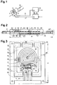
- 1 means a coin channel in a coin validator, 2 a coin, 3 a coil, 4 a detector circuit, 5 a feed device and 6 an evaluation unit.
- the supply device 6 is used for energy supply and is connected to the detector circuit 4 via supply lines 7 and to the evaluation unit 6 via supply lines 8.
- a signal line 9 extends from the detector circuit 4 to the evaluation unit 6 for transmitting measurement signals.
- the evaluation unit 6 analyzes the measurement signals in a predetermined manner and can release a service via a command line 10.
- the coin validator is e.g. B. in a public telephone or in a vending machine installed and enables the service to be triggered by means of coins 2.
- the coin validator comprises at least one inductive coin detector, which is formed from the coil 3 and the detector circuit 4 and as a scanning element on the coin channel 1 for measuring a predetermined size of the coin 2, such as the diameter of the coin 2, the type of coin alloy, etc., or for checking the presence of the Coin 2 in coin channel 1 is used.
- the coil 3 has at least one flat spiral conductor arrangement 11, so that the coil 3 can be arranged on the coin channel 1 in a space-saving manner.
- An alternating current in the conductor arrangement 11 of the coil 3 generates an alternating magnetic field which, in the direction of the coil axis 12 (FIG. 2), penetrates the coin channel 1 perpendicular to a running direction 13 of the coin 2, for example in such a way that the coil axis 12 is also parallel to the axis of the coin coin 2 moving past the coil 3 is aligned.
- the coil 3 (FIG. 1) has two flat spiral conductor arrangements 11 and 11 ′ which are coaxially aligned on both sides on an insulating film 14 and which can be electrically connected to one another by means of a through-connection 16 through the center 15 of the coil 3.
- the coil axis 12 shown in dashed lines is perpendicular to the plane of the conductor arrangement 11 or 11 'and penetrates the center 15.
- the conductor arrangement 11 or 11' winds from the center 15 around the coil axis 12 to the periphery of the conductor arrangement 11 or 11 ' and ends in a coil connection 17 and 18, respectively.
- Any electrical conductor material can be used for the conductor arrangement 11, 11 ', but copper is particularly inexpensive.
- the two conductor arrangements 11 and 11 ' can be connected to a through connection 16 to form a flat two-layer coil 3, the windings of which consist of the conductor arrangements 11 and 11'.
- both conductor arrangements 11 and 11 ' have the same winding sense on.
- the detector circuit 4 is arranged on the insulating film 14 outside the conductor arrangement 11.
- the coil connections 17, 18 of the two-layer coil 3 are connected to the detector circuit 4 via two short bridges 19, 19 ', one bridge 19' leading through the insulating film 14 to the other side to the coil connection 18.
- the detector circuit 4 has connection surfaces for contacting, which are connected via connections 20 to the connection lugs 21 for the feed lines 7 (FIG. 1) and the signal line 9 (FIG. 1).
- the coil 3 can also be made in one layer.
- the insulating film 14 can only carry the conductor arrangement 11 on one side or only the one conductor arrangement 11 or 11 ′ is connected, the through-connection 16 being missing.
- the bridges 19, 19 ′ end on the coil side in the center 15 and on the coil connection 17 or 18.
- the coin detector is advantageously housed in a flat housing 22.
- a stable, flat housing 22 can be produced inexpensively.
- the two flat sides 23, 23 'of the housing 22 are penetrated perpendicularly by the coil axis 12.
- the connection lugs 21 establish the connection to the feed lines 7 (FIG. 1) and the signal line 9 (FIG. 1) through the material of the housing 22. It is also possible to lead the supply lines 7 and the signal line 9 directly to the outside instead of the connection fields 21 as wire ends for direct connection to the supply device 5 (FIG. 1) and the evaluation unit 6 (FIG. 1), since there are already three wires for the necessary ones Lines 7, 9 between the coin detector and the power supply 5 and the evaluation unit 6 are sufficient.
- the detector circuit 4 is glued to a substrate 24 made of conductor material and, as shown in FIG. 3, comprises an oscillator circuit 25 and a measuring circuit 26.
- the oscillator circuit 25 in connection with the coil 3 (FIG. 1) forms an LC oscillator with the Coil 3 as an inductor. Examples of such LC oscillators are described in the book "Semiconductor Circuit Technology" by U. Tietze and Ch. Schenk, Springer-Verlag Berlin, 1978, ISBN 3-540-08628-5, pages 419 to 430, 4th edition.
- the alternating current generated by the oscillator circuit 25 in the coil 3 effects the alternating magnetic field of the coin detector in the coin channel 1 (FIG. 1). Without a coin 2 (FIG.
- the LC oscillator in the alternating magnetic field, the LC oscillator oscillates at a predetermined idle frequency f0. As soon as the material of the coin 2 draws energy from the alternating field, the frequency f of the LC oscillator changes.
- the LC oscillator of the coin detector begins to oscillate, the inductance of the coil 3 and a capacitor of the oscillator circuit 25 connected in parallel with the coil 3 determining the frequency f0. Since the coil 3 and the capacitor in the oscillator circuit 25 can be manufactured with very tight tolerances, the idle frequency f stre scatters in a narrow band, so that tuning of the LC oscillator to the predetermined idle frequency 0 is unnecessary.
- the coil 3 has an inductance of between 0.5 ⁇ H and 50 ⁇ H.
- the two-layer coil 3 with a predetermined diameter of 14 mm of both conductor arrangements 11, 11 ' has an inductance of 2920 nH with a total of 20 turns.
- the single-layer coil 3 has one conductor arrangement 11 of the same diameter and 10 turns only a quarter of the inductance, ie 730 nH.
- the coils 3 have a quality factor Q in the range from 5 to 10.
- the coin detector has the advantage that, because of the short bridges 19, 19 'between the oscillator circuit 25 and the coil 3, the LC oscillator can be constructed with little interference and because of the automatable manufacture, it can also be inexpensively constructed. In spite of the high frequencies f of the LC oscillator, the feed lines 7 and the signal line 9 do not emit any interfering electromagnetic waves which would impair the function of the coin validator and would further burden the LC oscillator.
- the compact coin detector is easy to place in the coin validator on coin channel 1 and is characterized by low power consumption.
- the coin detector can also be used generally as a sensor which detects an approach of a piece of metal with the alternating field of the coil 3.
- the oscillator circuit 25 and the measuring circuit 26 can be implemented on a Si wafer chip in CMOS technology. This measure lowers the current consumption of the detector circuit 4 to less than 30 ⁇ A at a supply voltage of 5 V when the LCO oscillator with the single-layer coil 3 oscillates at the idle frequency f0 of approximately 16 MHz.
- the insulating film 14 has the conductor arrangement 11 or 11 ′, the connecting tabs 21 and the substrate 24 on at least one side.
- These conductor pieces 11, 17, 21 and 24 or 11, 11 ', 17, 18, 21 and 24 made of an electrical conductor material can be applied to the insulating film 14 on one or both sides in a printing process or by vapor deposition or deposition.
- the step-by-step manufacture of the coin detectors is described below by way of example, the conductor pieces 11, 17, 21 and 24 or 11, 11 ', 17, 18, 21 and 24 are etched out of the conductor material laminated onto the insulating film 14 on one or both sides.
- the electrical conductor material has a thickness of 0.01 mm to 0.15 mm or more. The thicker conductor material brings about an advantageous rigidity of the connecting lugs 21.
- a tape 27 of a commercially available KAPTON (R) film 70 ⁇ m thick with a one- or both-sided layer of 17 ⁇ m copper can be used as the flexible insulating film 14.
- the coil 3 is produced as part of the “lead frame” together with the substrate 24 and the connecting tabs 21 from the band 27.
- the advantage of this method is its suitability for the automated manufacture of the coin detector, since all connections 16, 19, 19 ', 20 on the carrier sheet 30 can be carried out inexpensively by bonding thin wires if the detector circuit 4 is integrated on a semiconductor chip and the frequency-determining capacitor the oscillator circuit 25 is arranged as a separate component 25 'on the substrate 24 and is connected directly to the coil connections 17, 18.
- the coin detector can be adjusted between method steps f) and g), the value of the idle frequency f0 measured at the LC oscillator being stored in the measuring circuit 26 for the calculation of the frequency deviation ⁇ f.
- the manufacturing process can be for two-layer coils 3 are modified so that the conductor arrangements 11 are first produced on the belt 27 laminated on one side after the production steps a) to d). Subsequently, the conductor-free sides of two identical strips 27 treated in this way are aligned with the positioning holes 29, 29 'and joined to form a composite strip, the conductor arrangements 11 on both sides of the composite strip also being arranged coaxially and in the same winding direction.
- the composite strip is processed in the following manufacturing steps e) to h) like a double-sided tape 27.
Landscapes
- Physics & Mathematics (AREA)
- General Physics & Mathematics (AREA)
- Testing Of Coins (AREA)
- Pinball Game Machines (AREA)
- Noodles (AREA)
- Eye Examination Apparatus (AREA)
- Measurement Of Length, Angles, Or The Like Using Electric Or Magnetic Means (AREA)
Applications Claiming Priority (2)
| Application Number | Priority Date | Filing Date | Title |
|---|---|---|---|
| CH1782/92 | 1992-06-03 | ||
| CH178292 | 1992-06-03 |
Publications (2)
| Publication Number | Publication Date |
|---|---|
| EP0572847A1 true EP0572847A1 (fr) | 1993-12-08 |
| EP0572847B1 EP0572847B1 (fr) | 1998-08-26 |
Family
ID=4218484
Family Applications (1)
| Application Number | Title | Priority Date | Filing Date |
|---|---|---|---|
| EP93107938A Expired - Lifetime EP0572847B1 (fr) | 1992-06-03 | 1993-05-15 | Détecteur de pièces de monnaie |
Country Status (6)
| Country | Link |
|---|---|
| US (2) | US5411126A (fr) |
| EP (1) | EP0572847B1 (fr) |
| KR (1) | KR0165135B1 (fr) |
| AT (1) | ATE170312T1 (fr) |
| DE (1) | DE59308911D1 (fr) |
| DK (1) | DK0572847T3 (fr) |
Cited By (2)
| Publication number | Priority date | Publication date | Assignee | Title |
|---|---|---|---|---|
| EP0918306A3 (fr) * | 1997-11-19 | 1999-10-06 | Tetrel Limited | Systéme inductif de validation de piéces de monnaie et téléphone à paiement l'utilisant |
| DE10048290A1 (de) * | 2000-09-29 | 2002-05-08 | Balluff Gebhard Feinmech | Induktiver Sensor |
Families Citing this family (8)
| Publication number | Priority date | Publication date | Assignee | Title |
|---|---|---|---|---|
| DE19781532B4 (de) * | 1996-01-11 | 2008-01-17 | De La Rue Cash Systems, Inc., Watertown | Münzhandhabungsmaschine mit kreisförmiger Sortierplatte und Münzerkennung |
| ES2175441T3 (es) | 1996-07-29 | 2002-11-16 | Qvex Inc | Procedimiento y aparato de validacion de monedas. |
| US6896826B2 (en) * | 1997-01-09 | 2005-05-24 | Advanced Technology Materials, Inc. | Aqueous cleaning composition containing copper-specific corrosion inhibitor for cleaning inorganic residues on semiconductor substrate |
| JP2004227133A (ja) * | 2003-01-21 | 2004-08-12 | Internatl Currency Technologies Corp | 硬貨受け取り器の検出装置 |
| TWI227502B (en) | 2003-09-02 | 2005-02-01 | Ind Tech Res Inst | Precise multi-pole magnetic components and manufacturing method thereof |
| JP5924686B2 (ja) * | 2012-09-28 | 2016-05-25 | 株式会社日本コンラックス | 硬貨処理装置 |
| JP6992445B2 (ja) * | 2017-11-27 | 2022-01-13 | 富士電機株式会社 | 硬貨検知用アンテナおよび硬貨処理装置 |
| CN112406318B (zh) * | 2020-11-24 | 2023-07-21 | 武汉先同科技有限公司 | 一种基于电感技术的墨量检测装置、方法及喷墨打印机 |
Citations (5)
| Publication number | Priority date | Publication date | Assignee | Title |
|---|---|---|---|---|
| FR1532020A (fr) * | 1967-07-21 | 1968-07-05 | Scheidt & Bachmann Gmbh | Dispositif de vérification et de comptage de pièces de monnaie dans des distributeurs automatiques |
| US3901368A (en) * | 1974-03-11 | 1975-08-26 | Lance T Klinger | Coin acceptor/rejector |
| US4353453A (en) * | 1980-04-10 | 1982-10-12 | Atn Research & Development Corporation | Valid coin acceptor for coin actuated apparatus |
| US4441602A (en) * | 1981-12-02 | 1984-04-10 | Joseph Ostroski | Electronic coin verification mechanism |
| GB2174227A (en) * | 1985-04-15 | 1986-10-29 | Coin Controls | Apparatus for discriminating between different metallic articles |
Family Cites Families (10)
| Publication number | Priority date | Publication date | Assignee | Title |
|---|---|---|---|---|
| US3185947A (en) * | 1959-11-16 | 1965-05-25 | Arf Products | Inductive module for electronic devices |
| US3576244A (en) * | 1969-01-08 | 1971-04-27 | Vendo Co | Coin acceptor having resistivity and permeability detector |
| US4035695A (en) * | 1974-08-05 | 1977-07-12 | Motorola, Inc. | Microelectronic variable inductor |
| US4494100A (en) * | 1982-07-12 | 1985-01-15 | Motorola, Inc. | Planar inductors |
| US4574936A (en) * | 1983-05-10 | 1986-03-11 | Lance Klinger | Coin accepter/rejector including symmetrical dual feedback oscillator |
| EP0146251B1 (fr) * | 1983-11-04 | 1992-08-12 | Mars Incorporated | Dispositif de contrôle de validité de pièces de monnaie |
| US4678994A (en) * | 1984-06-27 | 1987-07-07 | Digital Products Corporation | Methods and apparatus employing apparent resonant properties of thin conducting materials |
| JPH0744405Y2 (ja) * | 1989-03-07 | 1995-10-11 | ローム株式会社 | プリント基板の切断装置 |
| EP0500367A3 (en) * | 1991-02-20 | 1993-07-21 | Telkor (Proprietary) Limited | Coil arrangement and static measuring device |
| US5133118A (en) * | 1991-08-06 | 1992-07-28 | Sheldahl, Inc. | Surface mounted components on flex circuits |
-
1993
- 1993-05-15 EP EP93107938A patent/EP0572847B1/fr not_active Expired - Lifetime
- 1993-05-15 DK DK93107938T patent/DK0572847T3/da active
- 1993-05-15 AT AT93107938T patent/ATE170312T1/de not_active IP Right Cessation
- 1993-05-15 DE DE59308911T patent/DE59308911D1/de not_active Expired - Fee Related
- 1993-05-17 US US08/072,913 patent/US5411126A/en not_active Expired - Fee Related
- 1993-06-01 KR KR1019930009794A patent/KR0165135B1/ko not_active Expired - Fee Related
-
1995
- 1995-03-24 US US08/410,066 patent/US5575057A/en not_active Expired - Fee Related
Patent Citations (5)
| Publication number | Priority date | Publication date | Assignee | Title |
|---|---|---|---|---|
| FR1532020A (fr) * | 1967-07-21 | 1968-07-05 | Scheidt & Bachmann Gmbh | Dispositif de vérification et de comptage de pièces de monnaie dans des distributeurs automatiques |
| US3901368A (en) * | 1974-03-11 | 1975-08-26 | Lance T Klinger | Coin acceptor/rejector |
| US4353453A (en) * | 1980-04-10 | 1982-10-12 | Atn Research & Development Corporation | Valid coin acceptor for coin actuated apparatus |
| US4441602A (en) * | 1981-12-02 | 1984-04-10 | Joseph Ostroski | Electronic coin verification mechanism |
| GB2174227A (en) * | 1985-04-15 | 1986-10-29 | Coin Controls | Apparatus for discriminating between different metallic articles |
Cited By (6)
| Publication number | Priority date | Publication date | Assignee | Title |
|---|---|---|---|---|
| EP0918306A3 (fr) * | 1997-11-19 | 1999-10-06 | Tetrel Limited | Systéme inductif de validation de piéces de monnaie et téléphone à paiement l'utilisant |
| US6539083B1 (en) | 1997-11-19 | 2003-03-25 | Marconi Communications Limited | Inductive coin validation system and payphone using such system |
| DE10048290A1 (de) * | 2000-09-29 | 2002-05-08 | Balluff Gebhard Feinmech | Induktiver Sensor |
| DE10048290C2 (de) * | 2000-09-29 | 2003-06-12 | Balluff Gmbh | Induktiver Sensor |
| US6734665B2 (en) | 2000-09-29 | 2004-05-11 | Balluff Gmbh | Inductive sensor having a sensor coil in the form of a structured conductive layer |
| DE10048290C5 (de) * | 2000-09-29 | 2005-12-08 | Balluff Gmbh | Induktiver Sensor |
Also Published As
| Publication number | Publication date |
|---|---|
| DK0572847T3 (da) | 1999-05-25 |
| KR940001014A (ko) | 1994-01-10 |
| US5411126A (en) | 1995-05-02 |
| KR0165135B1 (ko) | 1999-03-20 |
| US5575057A (en) | 1996-11-19 |
| EP0572847B1 (fr) | 1998-08-26 |
| DE59308911D1 (de) | 1998-10-01 |
| ATE170312T1 (de) | 1998-09-15 |
Similar Documents
| Publication | Publication Date | Title |
|---|---|---|
| DE60117080T2 (de) | Antenne | |
| DE60313930T2 (de) | Vorrichtung zur kontaktlosen Datenübertragung | |
| DE10220982B4 (de) | Sensor für schwach magnetische Felder unter Verwendung der Herstellungstechnik für gedruckte Leiterplatten und Verfahren zum Herstellen eines solchen Sensors | |
| EP0572847B1 (fr) | Détecteur de pièces de monnaie | |
| DE10330101A1 (de) | Sensor für schwache Magnetfelder, für den die Technologie der gedruckten Leiterplatten verwendet wird, und Verfahren zu seiner Herstellung | |
| DE4134397A1 (de) | Anordnung zum empfang von signalen von einem passiven transponder | |
| DE10325569A1 (de) | IC Karte und Verfahren zu ihrer Herstellung | |
| DE3616723A1 (de) | Mikrowellenbaustein | |
| DE4431604A1 (de) | Schaltungsanordnung mit einem Chipkartenmodul und einer damit verbundenen Spule | |
| DE69616697T2 (de) | Dielektrisches LC-Filter und Frequenzeinstellverfahren dafür | |
| DE19915074A1 (de) | Dielektrischer Resonator und dielektrisches Filter mit einem solchen Resonator | |
| DE10134184A1 (de) | Einheit zur Erfassung einer relativen Versetzung | |
| DE19651923C2 (de) | Sonde zur Erfassung von magnetischen Wechselfeldern | |
| EP0769792B1 (fr) | Bobine et procédé de sa connexion sur un support | |
| US4904973A (en) | Foil-roll electronic part | |
| DE3879518T2 (de) | Elektronisches bauelement mit rollenfolie und sein herstellungsverfahren. | |
| EP0561124B1 (fr) | Dispositif et méthode d'établissement de tentatives de fraudes d'un appareil de lecture et d'écriture d'une carte à puce | |
| DE102018215638B4 (de) | Bondfolie, elektronisches Bauelement und Verfahren zur Herstellung eines elektronischen Bauelements | |
| DE602004008334T2 (de) | Verbessertes resonanz-sicherheitsetikett und verfahren zur herstellung eines solchen etiketts | |
| KR100279729B1 (ko) | 적층형 칩 인덕터 | |
| DE3312680A1 (de) | Spulenanordnung | |
| EP0334988A2 (fr) | Détecteur de vibrations | |
| DE102022110670A1 (de) | Antennenvorrichtung und drahtlose energieübertragungsvorrichtung mit derselben | |
| US4908934A (en) | Process of producing a foil-roll electronic part | |
| DE2329488B2 (de) | Magnetischer Fühler mit einem parametrisch erregten zweiten harmonischen Oszillator |
Legal Events
| Date | Code | Title | Description |
|---|---|---|---|
| PUAI | Public reference made under article 153(3) epc to a published international application that has entered the european phase |
Free format text: ORIGINAL CODE: 0009012 |
|
| AK | Designated contracting states |
Kind code of ref document: A1 Designated state(s): AT CH DE DK FR LI NL SE |
|
| 17P | Request for examination filed |
Effective date: 19940111 |
|
| RAP1 | Party data changed (applicant data changed or rights of an application transferred) |
Owner name: LANDIS & GYR TECHNOLOGY INNOVATION AG |
|
| 17Q | First examination report despatched |
Effective date: 19951206 |
|
| GRAG | Despatch of communication of intention to grant |
Free format text: ORIGINAL CODE: EPIDOS AGRA |
|
| GRAG | Despatch of communication of intention to grant |
Free format text: ORIGINAL CODE: EPIDOS AGRA |
|
| GRAH | Despatch of communication of intention to grant a patent |
Free format text: ORIGINAL CODE: EPIDOS IGRA |
|
| GRAH | Despatch of communication of intention to grant a patent |
Free format text: ORIGINAL CODE: EPIDOS IGRA |
|
| GRAA | (expected) grant |
Free format text: ORIGINAL CODE: 0009210 |
|
| AK | Designated contracting states |
Kind code of ref document: B1 Designated state(s): AT CH DE DK FR LI NL SE |
|
| REF | Corresponds to: |
Ref document number: 170312 Country of ref document: AT Date of ref document: 19980915 Kind code of ref document: T |
|
| REG | Reference to a national code |
Ref country code: CH Ref legal event code: EP |
|
| REF | Corresponds to: |
Ref document number: 59308911 Country of ref document: DE Date of ref document: 19981001 |
|
| ET | Fr: translation filed | ||
| REG | Reference to a national code |
Ref country code: DK Ref legal event code: T3 |
|
| PLBE | No opposition filed within time limit |
Free format text: ORIGINAL CODE: 0009261 |
|
| 26N | No opposition filed | ||
| REG | Reference to a national code |
Ref country code: CH Ref legal event code: PUE Owner name: LANDIS & GYR TECHNOLOGY INNOVATION AG TRANSFER- IP Ref country code: CH Ref legal event code: NV Representative=s name: ELECTROWATT TECHNOLOGY INNOVATION AG C-IPR, 4470 |
|
| NLS | Nl: assignments of ep-patents |
Owner name: IP-TPG HOLDCO S.A.R.L. |
|
| NLT1 | Nl: modifications of names registered in virtue of documents presented to the patent office pursuant to art. 16 a, paragraph 1 |
Owner name: ELECTROWATT TECHNOLOGY INNOVATION AG |
|
| REG | Reference to a national code |
Ref country code: FR Ref legal event code: TP |
|
| REG | Reference to a national code |
Ref country code: CH Ref legal event code: NV Representative=s name: JOEL WENGER |
|
| PGFP | Annual fee paid to national office [announced via postgrant information from national office to epo] |
Ref country code: DK Payment date: 20010503 Year of fee payment: 9 |
|
| PG25 | Lapsed in a contracting state [announced via postgrant information from national office to epo] |
Ref country code: DK Free format text: LAPSE BECAUSE OF NON-PAYMENT OF DUE FEES Effective date: 20020531 |
|
| REG | Reference to a national code |
Ref country code: CH Ref legal event code: PUE Owner name: IP-TPG HOLDCO S.A.R.L. TRANSFER- IPM INTERNATIONAL Ref country code: CH Ref legal event code: NV Representative=s name: LEMAN CONSULTING S.A. |
|
| REG | Reference to a national code |
Ref country code: DK Ref legal event code: EBP |
|
| PGFP | Annual fee paid to national office [announced via postgrant information from national office to epo] |
Ref country code: CH Payment date: 20030422 Year of fee payment: 11 |
|
| PGFP | Annual fee paid to national office [announced via postgrant information from national office to epo] |
Ref country code: SE Payment date: 20030505 Year of fee payment: 11 |
|
| PGFP | Annual fee paid to national office [announced via postgrant information from national office to epo] |
Ref country code: NL Payment date: 20030506 Year of fee payment: 11 Ref country code: AT Payment date: 20030506 Year of fee payment: 11 |
|
| PGFP | Annual fee paid to national office [announced via postgrant information from national office to epo] |
Ref country code: FR Payment date: 20030512 Year of fee payment: 11 |
|
| PGFP | Annual fee paid to national office [announced via postgrant information from national office to epo] |
Ref country code: DE Payment date: 20030514 Year of fee payment: 11 |
|
| REG | Reference to a national code |
Ref country code: FR Ref legal event code: TP |
|
| PG25 | Lapsed in a contracting state [announced via postgrant information from national office to epo] |
Ref country code: AT Free format text: LAPSE BECAUSE OF NON-PAYMENT OF DUE FEES Effective date: 20040515 |
|
| PG25 | Lapsed in a contracting state [announced via postgrant information from national office to epo] |
Ref country code: SE Free format text: LAPSE BECAUSE OF NON-PAYMENT OF DUE FEES Effective date: 20040516 |
|
| PG25 | Lapsed in a contracting state [announced via postgrant information from national office to epo] |
Ref country code: LI Free format text: LAPSE BECAUSE OF NON-PAYMENT OF DUE FEES Effective date: 20040531 Ref country code: CH Free format text: LAPSE BECAUSE OF NON-PAYMENT OF DUE FEES Effective date: 20040531 |
|
| PG25 | Lapsed in a contracting state [announced via postgrant information from national office to epo] |
Ref country code: NL Free format text: LAPSE BECAUSE OF NON-PAYMENT OF DUE FEES Effective date: 20041201 Ref country code: DE Free format text: LAPSE BECAUSE OF NON-PAYMENT OF DUE FEES Effective date: 20041201 |
|
| EUG | Se: european patent has lapsed | ||
| REG | Reference to a national code |
Ref country code: CH Ref legal event code: PL |
|
| PG25 | Lapsed in a contracting state [announced via postgrant information from national office to epo] |
Ref country code: FR Free format text: LAPSE BECAUSE OF NON-PAYMENT OF DUE FEES Effective date: 20050131 |
|
| NLV4 | Nl: lapsed or anulled due to non-payment of the annual fee |
Effective date: 20041201 |
|
| REG | Reference to a national code |
Ref country code: FR Ref legal event code: ST |