EP0573348A1 - Verfahren zur Abscheidung von Kupfer auf ein Substrat und Vorrichtung zur Durchführung des Verfahrens - Google Patents
Verfahren zur Abscheidung von Kupfer auf ein Substrat und Vorrichtung zur Durchführung des Verfahrens Download PDFInfo
- Publication number
- EP0573348A1 EP0573348A1 EP93401398A EP93401398A EP0573348A1 EP 0573348 A1 EP0573348 A1 EP 0573348A1 EP 93401398 A EP93401398 A EP 93401398A EP 93401398 A EP93401398 A EP 93401398A EP 0573348 A1 EP0573348 A1 EP 0573348A1
- Authority
- EP
- European Patent Office
- Prior art keywords
- substrate
- metal
- gaseous
- production
- metal halide
- Prior art date
- Legal status (The legal status is an assumption and is not a legal conclusion. Google has not performed a legal analysis and makes no representation as to the accuracy of the status listed.)
- Granted
Links
- 239000000758 substrate Substances 0.000 title claims abstract description 71
- 238000000034 method Methods 0.000 title claims abstract description 40
- 230000008569 process Effects 0.000 title claims abstract description 9
- 239000010949 copper Substances 0.000 title claims description 45
- 229910052802 copper Inorganic materials 0.000 title claims description 43
- RYGMFSIKBFXOCR-UHFFFAOYSA-N Copper Chemical group [Cu] RYGMFSIKBFXOCR-UHFFFAOYSA-N 0.000 title claims description 42
- 230000008021 deposition Effects 0.000 title description 17
- 229910052751 metal Inorganic materials 0.000 claims abstract description 38
- 239000002184 metal Substances 0.000 claims abstract description 38
- 238000004519 manufacturing process Methods 0.000 claims abstract description 29
- 238000006243 chemical reaction Methods 0.000 claims abstract description 28
- 229910001507 metal halide Inorganic materials 0.000 claims abstract description 23
- 150000005309 metal halides Chemical class 0.000 claims abstract description 23
- 230000001603 reducing effect Effects 0.000 claims abstract description 17
- 239000007787 solid Substances 0.000 claims abstract description 14
- 238000010438 heat treatment Methods 0.000 claims abstract description 13
- 229910052736 halogen Inorganic materials 0.000 claims abstract description 12
- 150000002367 halogens Chemical class 0.000 claims abstract description 12
- 238000011065 in-situ storage Methods 0.000 claims abstract description 12
- 230000001105 regulatory effect Effects 0.000 claims abstract description 7
- 230000009467 reduction Effects 0.000 claims abstract description 6
- 239000007789 gas Substances 0.000 claims description 25
- 238000000151 deposition Methods 0.000 claims description 19
- 229910052710 silicon Inorganic materials 0.000 claims description 15
- 239000010703 silicon Substances 0.000 claims description 15
- 150000004820 halides Chemical class 0.000 claims description 11
- -1 SiHC1 3 Chemical compound 0.000 claims description 10
- 239000012159 carrier gas Substances 0.000 claims description 6
- 239000012808 vapor phase Substances 0.000 claims description 5
- 239000001257 hydrogen Substances 0.000 claims description 4
- 229910052739 hydrogen Inorganic materials 0.000 claims description 4
- 238000002347 injection Methods 0.000 claims description 4
- 239000007924 injection Substances 0.000 claims description 4
- ZOKXTWBITQBERF-UHFFFAOYSA-N Molybdenum Chemical compound [Mo] ZOKXTWBITQBERF-UHFFFAOYSA-N 0.000 claims description 3
- RTAQQCXQSZGOHL-UHFFFAOYSA-N Titanium Chemical compound [Ti] RTAQQCXQSZGOHL-UHFFFAOYSA-N 0.000 claims description 3
- 150000002431 hydrogen Chemical class 0.000 claims description 3
- 229910052750 molybdenum Inorganic materials 0.000 claims description 3
- 239000011733 molybdenum Substances 0.000 claims description 3
- 239000004033 plastic Substances 0.000 claims description 3
- 229920003023 plastic Polymers 0.000 claims description 3
- 229910052715 tantalum Inorganic materials 0.000 claims description 3
- GUVRBAGPIYLISA-UHFFFAOYSA-N tantalum atom Chemical compound [Ta] GUVRBAGPIYLISA-UHFFFAOYSA-N 0.000 claims description 3
- 239000010936 titanium Substances 0.000 claims description 3
- 229910052719 titanium Inorganic materials 0.000 claims description 3
- WFKWXMTUELFFGS-UHFFFAOYSA-N tungsten Chemical compound [W] WFKWXMTUELFFGS-UHFFFAOYSA-N 0.000 claims description 3
- 229910052721 tungsten Inorganic materials 0.000 claims description 3
- 239000010937 tungsten Substances 0.000 claims description 3
- 230000007935 neutral effect Effects 0.000 claims description 2
- 239000004065 semiconductor Substances 0.000 claims description 2
- 230000004907 flux Effects 0.000 abstract description 3
- XUIMIQQOPSSXEZ-UHFFFAOYSA-N Silicon Chemical compound [Si] XUIMIQQOPSSXEZ-UHFFFAOYSA-N 0.000 description 14
- 239000000460 chlorine Substances 0.000 description 8
- ZAMOUSCENKQFHK-UHFFFAOYSA-N Chlorine atom Chemical compound [Cl] ZAMOUSCENKQFHK-UHFFFAOYSA-N 0.000 description 7
- XKRFYHLGVUSROY-UHFFFAOYSA-N Argon Chemical compound [Ar] XKRFYHLGVUSROY-UHFFFAOYSA-N 0.000 description 6
- 238000005755 formation reaction Methods 0.000 description 6
- 238000001465 metallisation Methods 0.000 description 6
- 229910021591 Copper(I) chloride Inorganic materials 0.000 description 5
- 230000015572 biosynthetic process Effects 0.000 description 5
- 229910052801 chlorine Inorganic materials 0.000 description 5
- OXBLHERUFWYNTN-UHFFFAOYSA-M copper(I) chloride Chemical compound [Cu]Cl OXBLHERUFWYNTN-UHFFFAOYSA-M 0.000 description 5
- 238000001704 evaporation Methods 0.000 description 5
- 239000002243 precursor Substances 0.000 description 5
- VYPSYNLAJGMNEJ-UHFFFAOYSA-N Silicium dioxide Chemical compound O=[Si]=O VYPSYNLAJGMNEJ-UHFFFAOYSA-N 0.000 description 4
- 230000008020 evaporation Effects 0.000 description 4
- 230000003647 oxidation Effects 0.000 description 4
- 238000007254 oxidation reaction Methods 0.000 description 4
- 238000006722 reduction reaction Methods 0.000 description 4
- 229910052786 argon Inorganic materials 0.000 description 3
- 229910052799 carbon Inorganic materials 0.000 description 3
- 150000001875 compounds Chemical class 0.000 description 3
- XTVVROIMIGLXTD-UHFFFAOYSA-N copper(II) nitrate Chemical group [Cu+2].[O-][N+]([O-])=O.[O-][N+]([O-])=O XTVVROIMIGLXTD-UHFFFAOYSA-N 0.000 description 3
- 239000012535 impurity Substances 0.000 description 3
- 239000000376 reactant Substances 0.000 description 3
- 239000012265 solid product Substances 0.000 description 3
- 238000000859 sublimation Methods 0.000 description 3
- 230000008022 sublimation Effects 0.000 description 3
- QGZKDVFQNNGYKY-UHFFFAOYSA-N Ammonia Chemical compound N QGZKDVFQNNGYKY-UHFFFAOYSA-N 0.000 description 2
- OKTJSMMVPCPJKN-UHFFFAOYSA-N Carbon Chemical compound [C] OKTJSMMVPCPJKN-UHFFFAOYSA-N 0.000 description 2
- KZBUYRJDOAKODT-UHFFFAOYSA-N Chlorine Chemical compound ClCl KZBUYRJDOAKODT-UHFFFAOYSA-N 0.000 description 2
- VYZAMTAEIAYCRO-UHFFFAOYSA-N Chromium Chemical compound [Cr] VYZAMTAEIAYCRO-UHFFFAOYSA-N 0.000 description 2
- PXHVJJICTQNCMI-UHFFFAOYSA-N Nickel Chemical compound [Ni] PXHVJJICTQNCMI-UHFFFAOYSA-N 0.000 description 2
- QVGXLLKOCUKJST-UHFFFAOYSA-N atomic oxygen Chemical compound [O] QVGXLLKOCUKJST-UHFFFAOYSA-N 0.000 description 2
- 238000005229 chemical vapour deposition Methods 0.000 description 2
- 229910052804 chromium Inorganic materials 0.000 description 2
- 239000011651 chromium Substances 0.000 description 2
- 125000000058 cyclopentadienyl group Chemical group C1(=CC=CC1)* 0.000 description 2
- 238000000354 decomposition reaction Methods 0.000 description 2
- VNWKTOKETHGBQD-UHFFFAOYSA-N methane Chemical compound C VNWKTOKETHGBQD-UHFFFAOYSA-N 0.000 description 2
- 239000000203 mixture Substances 0.000 description 2
- 150000002902 organometallic compounds Chemical class 0.000 description 2
- 125000002524 organometallic group Chemical group 0.000 description 2
- 239000001301 oxygen Substances 0.000 description 2
- 229910052760 oxygen Inorganic materials 0.000 description 2
- 239000012071 phase Substances 0.000 description 2
- 238000005086 pumping Methods 0.000 description 2
- 239000010453 quartz Substances 0.000 description 2
- 229910052814 silicon oxide Inorganic materials 0.000 description 2
- 239000007858 starting material Substances 0.000 description 2
- SHXHPUAKLCCLDV-UHFFFAOYSA-N 1,1,1-trifluoropentane-2,4-dione Chemical compound CC(=O)CC(=O)C(F)(F)F SHXHPUAKLCCLDV-UHFFFAOYSA-N 0.000 description 1
- UGFAIRIUMAVXCW-UHFFFAOYSA-N Carbon monoxide Chemical compound [O+]#[C-] UGFAIRIUMAVXCW-UHFFFAOYSA-N 0.000 description 1
- UFHFLCQGNIYNRP-UHFFFAOYSA-N Hydrogen Chemical compound [H][H] UFHFLCQGNIYNRP-UHFFFAOYSA-N 0.000 description 1
- 229910052774 Proactinium Inorganic materials 0.000 description 1
- BQCADISMDOOEFD-UHFFFAOYSA-N Silver Chemical compound [Ag] BQCADISMDOOEFD-UHFFFAOYSA-N 0.000 description 1
- 241001080024 Telles Species 0.000 description 1
- 229910052782 aluminium Inorganic materials 0.000 description 1
- XAGFODPZIPBFFR-UHFFFAOYSA-N aluminium Chemical compound [Al] XAGFODPZIPBFFR-UHFFFAOYSA-N 0.000 description 1
- 150000001412 amines Chemical class 0.000 description 1
- 229910021529 ammonia Inorganic materials 0.000 description 1
- RBFQJDQYXXHULB-UHFFFAOYSA-N arsane Chemical class [AsH3] RBFQJDQYXXHULB-UHFFFAOYSA-N 0.000 description 1
- 229910002091 carbon monoxide Inorganic materials 0.000 description 1
- 238000004891 communication Methods 0.000 description 1
- 238000006471 dimerization reaction Methods 0.000 description 1
- 235000021183 entrée Nutrition 0.000 description 1
- 238000005530 etching Methods 0.000 description 1
- PCHJSUWPFVWCPO-UHFFFAOYSA-N gold Chemical compound [Au] PCHJSUWPFVWCPO-UHFFFAOYSA-N 0.000 description 1
- 229910052737 gold Inorganic materials 0.000 description 1
- 239000010931 gold Substances 0.000 description 1
- 239000001307 helium Substances 0.000 description 1
- 229910052734 helium Inorganic materials 0.000 description 1
- SWQJXJOGLNCZEY-UHFFFAOYSA-N helium atom Chemical compound [He] SWQJXJOGLNCZEY-UHFFFAOYSA-N 0.000 description 1
- QWPPOHNGKGFGJK-UHFFFAOYSA-N hypochlorous acid Chemical compound ClO QWPPOHNGKGFGJK-UHFFFAOYSA-N 0.000 description 1
- 239000012212 insulator Substances 0.000 description 1
- 239000003446 ligand Substances 0.000 description 1
- 150000002739 metals Chemical class 0.000 description 1
- 229910052759 nickel Inorganic materials 0.000 description 1
- 239000002245 particle Substances 0.000 description 1
- 150000003003 phosphines Chemical class 0.000 description 1
- 238000000206 photolithography Methods 0.000 description 1
- 239000000843 powder Substances 0.000 description 1
- 239000000047 product Substances 0.000 description 1
- 229910052709 silver Inorganic materials 0.000 description 1
- 239000004332 silver Substances 0.000 description 1
- 239000007790 solid phase Substances 0.000 description 1
- 238000004544 sputter deposition Methods 0.000 description 1
- 239000000126 substance Substances 0.000 description 1
- 238000007740 vapor deposition Methods 0.000 description 1
Images
Classifications
-
- C—CHEMISTRY; METALLURGY
- C23—COATING METALLIC MATERIAL; COATING MATERIAL WITH METALLIC MATERIAL; CHEMICAL SURFACE TREATMENT; DIFFUSION TREATMENT OF METALLIC MATERIAL; COATING BY VACUUM EVAPORATION, BY SPUTTERING, BY ION IMPLANTATION OR BY CHEMICAL VAPOUR DEPOSITION, IN GENERAL; INHIBITING CORROSION OF METALLIC MATERIAL OR INCRUSTATION IN GENERAL
- C23C—COATING METALLIC MATERIAL; COATING MATERIAL WITH METALLIC MATERIAL; SURFACE TREATMENT OF METALLIC MATERIAL BY DIFFUSION INTO THE SURFACE, BY CHEMICAL CONVERSION OR SUBSTITUTION; COATING BY VACUUM EVAPORATION, BY SPUTTERING, BY ION IMPLANTATION OR BY CHEMICAL VAPOUR DEPOSITION, IN GENERAL
- C23C16/00—Chemical coating by decomposition of gaseous compounds, without leaving reaction products of surface material in the coating, i.e. chemical vapour deposition [CVD] processes
- C23C16/06—Chemical coating by decomposition of gaseous compounds, without leaving reaction products of surface material in the coating, i.e. chemical vapour deposition [CVD] processes characterised by the deposition of metallic material
- C23C16/08—Chemical coating by decomposition of gaseous compounds, without leaving reaction products of surface material in the coating, i.e. chemical vapour deposition [CVD] processes characterised by the deposition of metallic material from metal halides
- C23C16/14—Deposition of only one other metal element
-
- C—CHEMISTRY; METALLURGY
- C23—COATING METALLIC MATERIAL; COATING MATERIAL WITH METALLIC MATERIAL; CHEMICAL SURFACE TREATMENT; DIFFUSION TREATMENT OF METALLIC MATERIAL; COATING BY VACUUM EVAPORATION, BY SPUTTERING, BY ION IMPLANTATION OR BY CHEMICAL VAPOUR DEPOSITION, IN GENERAL; INHIBITING CORROSION OF METALLIC MATERIAL OR INCRUSTATION IN GENERAL
- C23C—COATING METALLIC MATERIAL; COATING MATERIAL WITH METALLIC MATERIAL; SURFACE TREATMENT OF METALLIC MATERIAL BY DIFFUSION INTO THE SURFACE, BY CHEMICAL CONVERSION OR SUBSTITUTION; COATING BY VACUUM EVAPORATION, BY SPUTTERING, BY ION IMPLANTATION OR BY CHEMICAL VAPOUR DEPOSITION, IN GENERAL
- C23C16/00—Chemical coating by decomposition of gaseous compounds, without leaving reaction products of surface material in the coating, i.e. chemical vapour deposition [CVD] processes
- C23C16/44—Chemical coating by decomposition of gaseous compounds, without leaving reaction products of surface material in the coating, i.e. chemical vapour deposition [CVD] processes characterised by the method of coating
- C23C16/448—Chemical coating by decomposition of gaseous compounds, without leaving reaction products of surface material in the coating, i.e. chemical vapour deposition [CVD] processes characterised by the method of coating characterised by the method used for generating reactive gas streams, e.g. by evaporation or sublimation of precursor materials
- C23C16/4488—Chemical coating by decomposition of gaseous compounds, without leaving reaction products of surface material in the coating, i.e. chemical vapour deposition [CVD] processes characterised by the method of coating characterised by the method used for generating reactive gas streams, e.g. by evaporation or sublimation of precursor materials by in situ generation of reactive gas by chemical or electrochemical reaction
Definitions
- the present invention relates to a method of vapor deposition of a metal (such as copper, tungsten, titanium, tantalum, molybdenum) on a substrate, as well as to a device for carrying out this method.
- a metal such as copper, tungsten, titanium, tantalum, molybdenum
- the chemical vapor metal deposition (CVD) method is widely used to produce thin layers of good quality metal; this method has found application in many industries, especially in the electronics industry.
- these layers are usually produced under vacuum, by thermo-evaporation or else by sputtering; the deposit can be made either on the entire surface of the substrate, then engraved, or through a mask, so as to directly obtain the desired design.
- European Patent Application EP 297 348 in the name of IBM, describes a method of chemical vapor deposition of copper (CVD technique), using as starting material or precursor, an organometallic complex of the cyclopentadienylmetal type, in gaseous form and comprising a cyclopentadienyl nucleus, a donor ligand of two electrons (trivalent phosphines, amines and arsines) and a metal from group IB in an oxidation state +1.
- CVD technique chemical vapor deposition of copper (CVD technique)
- an organometallic complex of the cyclopentadienylmetal type in gaseous form and comprising a cyclopentadienyl nucleus, a donor ligand of two electrons (trivalent phosphines, amines and arsines) and a metal from group IB in an oxidation state +1.
- the substrate on which the deposit is to be made is heated, so that the reaction of decomposition of the vapors of the precursor complex takes place at said substrate and leads to the deposition of the metal (group IB) at said substrate.
- organometallic precursors such as compounds of the trifluoroacetylacetone or hexafluoroacetylacetonate type.
- US Patent 4,842,891 in the name of HITACHI LTD, describes a method of forming a copper layer by CVD, in which the starting product is copper nitrate.
- the copper nitrate vapor is reduced with a low molecular weight reducing gas such as carbon monoxide, hydrogen, methane, ammonia, so that metallic copper is precipitated on the surface of the substrate, maintained at a temperature of 200-650 ° C.
- the reaction conditions are more particularly described: the pressure in the reaction chamber must be between 0.1 and 3 torr and the copper nitrate / reducing gas ratio is greater than a stoichiometric ratio.
- the first CVD techniques described used CuCI 2 (oxidation state +2) at temperatures between 400 and 1200 ° C and had the disadvantage of having excessive reaction temperatures.
- the CuCI was evaporated at a temperature between 300 and 350 ° C and the deposition temperatures were between 350 and 500 ° C.
- Copper deposits on a Si0 2 substrate (evaporation temperature: 350 ° C; deformation temperature pot: 500 ° C; partial pressure of CuCI: 1.2 Pa, in the presence of hydrogen as reducing gas), with an average thickness of 1.5 ⁇ m, are deposited in 5 h, which corresponds to a deposition rate of approximately 0.3 wm / h.
- the method exposed in this article has the disadvantage of causing a deposit of poor quality (impurities), at too low a speed (0.3 ⁇ m / h) for an industrial application.
- the present invention has therefore set itself the aim of providing a CVD metal deposition process, which better meets the needs of the practice than the methods currently used, by enabling a deposition rate of a few to be obtained. micrometers per minute, under conditions of pressure and temperature particularly well suited to the substrates to be treated and allowing the homogeneous or selective deposition of a layer of good quality metal.
- the metal is chosen from copper, tungsten, titanium, tantalum and molybdenum.
- the reducing gas is chosen from the group comprising hydrogen, SiH 4 , Si 2 H s , Si 3 H 8 , SiH 2 CI 2 , SiHC1 3 , SiH 3 Cl.
- the substrate is chosen from the group which comprises semiconductor substrates, in particular based on silicon and plastic substrates.
- the deposit can be homogeneous or selective.
- a deposit in a homogeneous layer is obtained on the order of ⁇ m / min.
- said layer of metal is deposited selectively at certain zones , silicon or metal, only.
- a deposit of metal (copper in particular) is observed, only in the areas of bare silicon while the metal does not deposit in the areas of oxidized silicon.
- selectivity is also observed with substrates where part of the surface is oxidized, the rest of the surface being covered with a metal, copper or chromium, for example.
- Such a method is particularly advantageous in the metallization of the last interconnection levels of integrated circuits, in the production of interconnection networks for hybrid circuits, as well as in the metallization of plastics.
- the reactive gases are associated with a neutral carrier gas.
- this carrier gas which can advantageously be argon, ensures the transport of the reactive gases and avoids a reaction in homogeneous phase; its partial pressure advantageously represents approximately 80% of the total pressure.
- the regulation of gas flows is ensured by mass flow meters.
- said means for producing gaseous metal halide surrounds said substrate and allows uniform radial injection of the halide on the substrate.
- said means for producing gaseous metal halide further comprises a source of carrier gas.
- such a device makes it possible to produce, in the case of copper, for example, a source of gaseous CuCl with an adjustable flow rate, cardan the temperature and pressure conditions as defined in the process according to the invention, the kinetics of CuCI formation, from C1 2 gas and solid copper, is defined and controllable; indeed, such a device, allowing a radial and therefore uniform injection of the copper halide, results in a concentration in the vapor phase which is sufficiently large to obtain metal deposition rates of the order of a micrometer per minute.
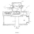
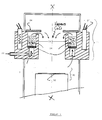
- FIG. 1 represents a device according to the invention, in longitudinal section, which advantageously comprises a reaction chamber 10, including both a means for producing gaseous copper halide 11 and a zone for depositing copper 12 on a substrate 30.
- This means for producing gaseous copper halide 11 allows said halide to be injected into the actual reaction chamber, in its central part X-X, also maintained at a temperature of approximately 250 ° C.
- the flow rate of gaseous CuCI is controlled by the flow rate of chlorine sent into the means 11.
- the CuCi formed is located in the vicinity of the substrate 30 and is brought into contact with a reducing gas or a mixture of reducing gases, sent to the reaction chamber 10, via the conduit 23, which opens from the outside of said reaction chamber 10, just above the substrate 30; the inlet flow rates of said reducing gases are regulated using mass flowmeters.
- the device according to the invention has the advantage of providing a source of halide produced in situ, integral with the reaction chamber.
- the regulation of the flow of chlorine injected into said means allows, for temperatures above 350 ° C. , precise control of the flow rate of Cu 3 Cl 3 brought into contact with the substrate and therefore a concentration of the latter in the vapor phase sufficiently large to obtain copper deposition rates of the order of a micrometer per minute.
- the injection of the reactant (CuCI) at the level of the copper deposition zone 12 is carried out through a series of orifices, uniformly distributed over the perimeter surrounding the substrate 30 (not shown in FIGS. 1 and 2), ensuring communication between the halide production means 11 and the deposition zone 12.
- EXAMPLE 1 Implementation of the method: deposition of copper on a substrate with heterogeneous zones, in a device as described in FIGS. 1 and 2.
- a substrate having zones of silicon and zones of silicon oxide makes it possible, under the conditions defined below, to selectively obtain a deposit of copper on the silicon only.
- the resistivity value measured is approximately 2 ⁇ ohms cm-1, a value close to that of solid copper. This is in particular due to the absence of solid reactants which can become trapped in the copper as well as to the high vapor pressure of the gaseous reactants eliminated by pumping.
- EXAMPLE 2 Deposition of copper on a homogeneous substrate.
Landscapes
- Chemical & Material Sciences (AREA)
- General Chemical & Material Sciences (AREA)
- Chemical Kinetics & Catalysis (AREA)
- Engineering & Computer Science (AREA)
- Materials Engineering (AREA)
- Mechanical Engineering (AREA)
- Metallurgy (AREA)
- Organic Chemistry (AREA)
- Electrochemistry (AREA)
- Chemical Vapour Deposition (AREA)
- Electrodes Of Semiconductors (AREA)
Applications Claiming Priority (2)
| Application Number | Priority Date | Filing Date | Title |
|---|---|---|---|
| FR9206706A FR2691984B1 (fr) | 1992-06-03 | 1992-06-03 | Procédé de dépôt de métal sur un substrat et dispositif pour sa mise en Óoeuvre. |
| FR9206706 | 1992-06-03 |
Publications (2)
| Publication Number | Publication Date |
|---|---|
| EP0573348A1 true EP0573348A1 (de) | 1993-12-08 |
| EP0573348B1 EP0573348B1 (de) | 1997-03-26 |
Family
ID=9430386
Family Applications (1)
| Application Number | Title | Priority Date | Filing Date |
|---|---|---|---|
| EP19930401398 Expired - Lifetime EP0573348B1 (de) | 1992-06-03 | 1993-06-02 | Verfahren zur Abscheidung von Kupfer auf ein Substrat und Vorrichtung zur Durchführung des Verfahrens |
Country Status (3)
| Country | Link |
|---|---|
| EP (1) | EP0573348B1 (de) |
| DE (1) | DE69309154T2 (de) |
| FR (1) | FR2691984B1 (de) |
Cited By (7)
| Publication number | Priority date | Publication date | Assignee | Title |
|---|---|---|---|---|
| WO2001077407A1 (en) * | 2000-04-05 | 2001-10-18 | Tokyo Electron Limited | In-situ generation of precursors for cvd |
| US6656540B2 (en) * | 2000-03-27 | 2003-12-02 | Mitsubishi Heavy Industries, Ltd. | Method for forming metallic film and apparatus for forming the same |
| EP1284305A3 (de) * | 2001-08-08 | 2004-01-07 | Mitsubishi Heavy Industries, Ltd. | Verfahren und Vorrichtung zur Dampfabscheidung eines Kupferfilms |
| EP1312696A3 (de) * | 2001-11-14 | 2004-01-07 | Mitsubishi Heavy Industries, Ltd. | Vorrichtung und Methode zur Herstellung von Barriereschichten für Metalle sowie Vorrichtung und Methode zur Herstellung von Metallschichten |
| US7279201B2 (en) * | 2001-04-07 | 2007-10-09 | Aviza Europe Limited | Methods and apparatus for forming precursors |
| US7659209B2 (en) | 2001-11-14 | 2010-02-09 | Canon Anelva Corporation | Barrier metal film production method |
| CN117684151A (zh) * | 2023-12-27 | 2024-03-12 | 电子科技大学中山学院 | 一种化学气相沉积装置以及方法 |
Citations (5)
| Publication number | Priority date | Publication date | Assignee | Title |
|---|---|---|---|---|
| US3787236A (en) * | 1971-11-11 | 1974-01-22 | United Aircraft Corp | Tungsten coated glass fiber |
| US4239819A (en) * | 1978-12-11 | 1980-12-16 | Chemetal Corporation | Deposition method and products |
| GB2057018A (en) * | 1979-07-26 | 1981-03-25 | Us Energy | Refractory metal coated multi-filament yarn |
| JPS63250463A (ja) * | 1987-04-08 | 1988-10-18 | Ulvac Corp | 金属薄膜形成方法 |
| EP0482265A1 (de) * | 1989-10-12 | 1992-04-29 | L'air Liquide, Societe Anonyme Pour L'etude Et L'exploitation Des Procedes Georges Claude | Verfahren zum Herstellen einer Kupfer-Dünnschicht mittels chemischer Gasphasenabscheidung bei Niedrigtemperatur |
-
1992
- 1992-06-03 FR FR9206706A patent/FR2691984B1/fr not_active Expired - Fee Related
-
1993
- 1993-06-02 EP EP19930401398 patent/EP0573348B1/de not_active Expired - Lifetime
- 1993-06-02 DE DE1993609154 patent/DE69309154T2/de not_active Expired - Fee Related
Patent Citations (5)
| Publication number | Priority date | Publication date | Assignee | Title |
|---|---|---|---|---|
| US3787236A (en) * | 1971-11-11 | 1974-01-22 | United Aircraft Corp | Tungsten coated glass fiber |
| US4239819A (en) * | 1978-12-11 | 1980-12-16 | Chemetal Corporation | Deposition method and products |
| GB2057018A (en) * | 1979-07-26 | 1981-03-25 | Us Energy | Refractory metal coated multi-filament yarn |
| JPS63250463A (ja) * | 1987-04-08 | 1988-10-18 | Ulvac Corp | 金属薄膜形成方法 |
| EP0482265A1 (de) * | 1989-10-12 | 1992-04-29 | L'air Liquide, Societe Anonyme Pour L'etude Et L'exploitation Des Procedes Georges Claude | Verfahren zum Herstellen einer Kupfer-Dünnschicht mittels chemischer Gasphasenabscheidung bei Niedrigtemperatur |
Non-Patent Citations (1)
| Title |
|---|
| PATENT ABSTRACTS OF JAPAN vol. 13, no. 61 (C - 567)<3409> 10 February 1989 (1989-02-10) * |
Cited By (11)
| Publication number | Priority date | Publication date | Assignee | Title |
|---|---|---|---|---|
| US6656540B2 (en) * | 2000-03-27 | 2003-12-02 | Mitsubishi Heavy Industries, Ltd. | Method for forming metallic film and apparatus for forming the same |
| EP1199378A4 (de) * | 2000-03-27 | 2006-09-20 | Mitsubishi Heavy Ind Ltd | Verfahren und vorrichtung zur herstellung eines metallfilms |
| WO2001077407A1 (en) * | 2000-04-05 | 2001-10-18 | Tokyo Electron Limited | In-situ generation of precursors for cvd |
| US6440494B1 (en) | 2000-04-05 | 2002-08-27 | Tokyo Electron Limited | In-situ source synthesis for metal CVD |
| US7279201B2 (en) * | 2001-04-07 | 2007-10-09 | Aviza Europe Limited | Methods and apparatus for forming precursors |
| EP1284305A3 (de) * | 2001-08-08 | 2004-01-07 | Mitsubishi Heavy Industries, Ltd. | Verfahren und Vorrichtung zur Dampfabscheidung eines Kupferfilms |
| US7048973B2 (en) | 2001-08-08 | 2006-05-23 | Mitsubishi Heavy Industries, Ltd. | Metal film vapor phase deposition method and vapor phase deposition apparatus |
| EP1312696A3 (de) * | 2001-11-14 | 2004-01-07 | Mitsubishi Heavy Industries, Ltd. | Vorrichtung und Methode zur Herstellung von Barriereschichten für Metalle sowie Vorrichtung und Methode zur Herstellung von Metallschichten |
| US7659209B2 (en) | 2001-11-14 | 2010-02-09 | Canon Anelva Corporation | Barrier metal film production method |
| US7977243B2 (en) | 2001-11-14 | 2011-07-12 | Canon Anelva Corporation | Barrier metal film production apparatus, barrier metal film production method, metal film production method, and metal film production apparatus |
| CN117684151A (zh) * | 2023-12-27 | 2024-03-12 | 电子科技大学中山学院 | 一种化学气相沉积装置以及方法 |
Also Published As
| Publication number | Publication date |
|---|---|
| FR2691984A1 (fr) | 1993-12-10 |
| EP0573348B1 (de) | 1997-03-26 |
| DE69309154T2 (de) | 1997-07-10 |
| FR2691984B1 (fr) | 1995-03-24 |
| DE69309154D1 (de) | 1997-04-30 |
Similar Documents
| Publication | Publication Date | Title |
|---|---|---|
| TW309628B (de) | ||
| US5273775A (en) | Process for selectively depositing copper aluminum alloy onto a substrate | |
| EP3068725B1 (de) | Verfahren zur kontinuierlichen herstellung von auf einem substrat ausgerichteten nanostrukturen und zugehörige vorrichtung | |
| FR2554132A1 (fr) | Procede de depot de siliciure metallique par depot de vapeur chimique, exalte par du plasma | |
| FR1467105A (fr) | Procédé de fabrication d'une couche monocristalline de carbure de silicium | |
| US20060264038A1 (en) | Method for forming barrier film and method for forming electrode film | |
| EP0573348B1 (de) | Verfahren zur Abscheidung von Kupfer auf ein Substrat und Vorrichtung zur Durchführung des Verfahrens | |
| US20060225162A1 (en) | Method of making a substrate structure with enhanced surface area | |
| EP0001373A1 (de) | Verfahren zur Erzeugung von glatten und fehlerfreien dünnen Siliciumcarbidschichten auf einem Siliciumsubstrat | |
| EP0143701A1 (de) | Verfahren zur Abscheidung von amorphem Silizium durch thermische Zersetzung bei niedriger Temperatur und Vorrichtung zur Durchführung des Verfahrens | |
| FR2995618A1 (fr) | Procede de traitement de surface de monocristaux de materiaux | |
| EP3763846A1 (de) | Verfahren zur herstellung eines vanadiumdisulfid-films und anhand dieses verfahrens erhältlicher film | |
| EP1606429B1 (de) | Verfahren zur cvd-abscheidung eines silberfilms auf einem substrat | |
| FR2573917A1 (fr) | Appareil et procede de depot a la vapeur pour la realisation de semi-conducteurs | |
| CH678176A5 (de) | ||
| CN113699503B (zh) | 金属表面具有多相复合碳源的石墨烯制备方法及装置 | |
| JP2000511705A (ja) | 半導体デバイスの製造方法及びこの方法を実施する装置 | |
| EP0386190A1 (de) | Elementare quecksilberquelle für metall-organische chemische abscheidung aus der gasphase. | |
| JP2887240B2 (ja) | 薄膜成長方法および装置 | |
| EP0538143B1 (de) | Anorganische Filtrationsmembrane mit im wesentlichen sauerstoffreier keramischer Trennschicht | |
| EP1411143A1 (de) | Verfahren zum Herstellung von rohrförmigen Hohlkörpern mit innenseitiger Diamantbeschichtung | |
| JP2649693B2 (ja) | 気相成長装置 | |
| EP3632845A1 (de) | Mehrschichtstapelung für das schichtwachstum durch chemische gasphasenabscheidung von kohlenstoffnanoröhren | |
| WO2005009900A2 (fr) | Procede de fabrication de nanocomposes de carbone graphitique et en particulier de nanoperles, en vrac ou de façon individualisee | |
| FR2738017A1 (fr) | Procede de revetement d'un carbure ou d'un carbonitrure mixte de ti et de zr par depot chimique en phase vapeur (cvd) et dispositif destine a former un revetement ceramique a partir d'au moins deux precurseurs metalliques |
Legal Events
| Date | Code | Title | Description |
|---|---|---|---|
| PUAI | Public reference made under article 153(3) epc to a published international application that has entered the european phase |
Free format text: ORIGINAL CODE: 0009012 |
|
| AK | Designated contracting states |
Kind code of ref document: A1 Designated state(s): DE GB |
|
| 17P | Request for examination filed |
Effective date: 19940525 |
|
| 17Q | First examination report despatched |
Effective date: 19940228 |
|
| RAP1 | Party data changed (applicant data changed or rights of an application transferred) |
Owner name: CENTRE NATIONAL DE LA RECHERCHE SCIENTIFIQUE (CNR Owner name: FRANCE TELECOM |
|
| GRAG | Despatch of communication of intention to grant |
Free format text: ORIGINAL CODE: EPIDOS AGRA |
|
| GRAH | Despatch of communication of intention to grant a patent |
Free format text: ORIGINAL CODE: EPIDOS IGRA |
|
| GRAH | Despatch of communication of intention to grant a patent |
Free format text: ORIGINAL CODE: EPIDOS IGRA |
|
| GRAA | (expected) grant |
Free format text: ORIGINAL CODE: 0009210 |
|
| AK | Designated contracting states |
Kind code of ref document: B1 Designated state(s): DE GB |
|
| REF | Corresponds to: |
Ref document number: 69309154 Country of ref document: DE Date of ref document: 19970430 |
|
| GBT | Gb: translation of ep patent filed (gb section 77(6)(a)/1977) |
Effective date: 19970421 |
|
| PLBE | No opposition filed within time limit |
Free format text: ORIGINAL CODE: 0009261 |
|
| STAA | Information on the status of an ep patent application or granted ep patent |
Free format text: STATUS: NO OPPOSITION FILED WITHIN TIME LIMIT |
|
| 26N | No opposition filed | ||
| REG | Reference to a national code |
Ref country code: GB Ref legal event code: IF02 |
|
| PGFP | Annual fee paid to national office [announced via postgrant information from national office to epo] |
Ref country code: DE Payment date: 20040526 Year of fee payment: 12 |
|
| PGFP | Annual fee paid to national office [announced via postgrant information from national office to epo] |
Ref country code: GB Payment date: 20040602 Year of fee payment: 12 |
|
| PG25 | Lapsed in a contracting state [announced via postgrant information from national office to epo] |
Ref country code: GB Free format text: LAPSE BECAUSE OF NON-PAYMENT OF DUE FEES Effective date: 20050602 |
|
| PG25 | Lapsed in a contracting state [announced via postgrant information from national office to epo] |
Ref country code: DE Free format text: LAPSE BECAUSE OF NON-PAYMENT OF DUE FEES Effective date: 20060103 |
|
| GBPC | Gb: european patent ceased through non-payment of renewal fee |
Effective date: 20050602 |