EP0573370A1 - Système d'imprimante des points à densité variable avec utilisation des matrices de sous-micropoint et d'un objectif zoom - Google Patents
Système d'imprimante des points à densité variable avec utilisation des matrices de sous-micropoint et d'un objectif zoom Download PDFInfo
- Publication number
- EP0573370A1 EP0573370A1 EP93420218A EP93420218A EP0573370A1 EP 0573370 A1 EP0573370 A1 EP 0573370A1 EP 93420218 A EP93420218 A EP 93420218A EP 93420218 A EP93420218 A EP 93420218A EP 0573370 A1 EP0573370 A1 EP 0573370A1
- Authority
- EP
- European Patent Office
- Prior art keywords
- laser
- microdot
- predetermined
- lasers
- address
- Prior art date
- Legal status (The legal status is an assumption and is not a legal conclusion. Google has not performed a legal analysis and makes no representation as to the accuracy of the status listed.)
- Granted
Links
Images


Classifications
-
- H—ELECTRICITY
- H04—ELECTRIC COMMUNICATION TECHNIQUE
- H04N—PICTORIAL COMMUNICATION, e.g. TELEVISION
- H04N1/00—Scanning, transmission or reproduction of documents or the like, e.g. facsimile transmission; Details thereof
- H04N1/04—Scanning arrangements, i.e. arrangements for the displacement of active reading or reproducing elements relative to the original or reproducing medium, or vice versa
- H04N1/19—Scanning arrangements, i.e. arrangements for the displacement of active reading or reproducing elements relative to the original or reproducing medium, or vice versa using multi-element arrays
- H04N1/191—Scanning arrangements, i.e. arrangements for the displacement of active reading or reproducing elements relative to the original or reproducing medium, or vice versa using multi-element arrays the array comprising a one-dimensional [1D] array
- H04N1/1911—Simultaneously or substantially simultaneously scanning picture elements on more than one main scanning line, e.g. scanning in swaths
-
- H—ELECTRICITY
- H04—ELECTRIC COMMUNICATION TECHNIQUE
- H04N—PICTORIAL COMMUNICATION, e.g. TELEVISION
- H04N1/00—Scanning, transmission or reproduction of documents or the like, e.g. facsimile transmission; Details thereof
- H04N1/04—Scanning arrangements, i.e. arrangements for the displacement of active reading or reproducing elements relative to the original or reproducing medium, or vice versa
- H04N1/0402—Scanning different formats; Scanning with different densities of dots per unit length, e.g. different numbers of dots per inch (dpi); Conversion of scanning standards
- H04N1/0408—Different densities of dots per unit length
- H04N1/0411—Different densities of dots per unit length in the main scanning direction
-
- H—ELECTRICITY
- H04—ELECTRIC COMMUNICATION TECHNIQUE
- H04N—PICTORIAL COMMUNICATION, e.g. TELEVISION
- H04N1/00—Scanning, transmission or reproduction of documents or the like, e.g. facsimile transmission; Details thereof
- H04N1/04—Scanning arrangements, i.e. arrangements for the displacement of active reading or reproducing elements relative to the original or reproducing medium, or vice versa
- H04N1/0402—Scanning different formats; Scanning with different densities of dots per unit length, e.g. different numbers of dots per inch (dpi); Conversion of scanning standards
- H04N1/042—Details of the method used
- H04N1/0432—Varying the magnification of a single lens group
-
- H—ELECTRICITY
- H04—ELECTRIC COMMUNICATION TECHNIQUE
- H04N—PICTORIAL COMMUNICATION, e.g. TELEVISION
- H04N1/00—Scanning, transmission or reproduction of documents or the like, e.g. facsimile transmission; Details thereof
- H04N1/04—Scanning arrangements, i.e. arrangements for the displacement of active reading or reproducing elements relative to the original or reproducing medium, or vice versa
- H04N1/06—Scanning arrangements, i.e. arrangements for the displacement of active reading or reproducing elements relative to the original or reproducing medium, or vice versa using cylindrical picture-bearing surfaces, i.e. scanning a main-scanning line substantially perpendicular to the axis and lying in a curved cylindrical surface
- H04N1/0671—Scanning arrangements, i.e. arrangements for the displacement of active reading or reproducing elements relative to the original or reproducing medium, or vice versa using cylindrical picture-bearing surfaces, i.e. scanning a main-scanning line substantially perpendicular to the axis and lying in a curved cylindrical surface with sub-scanning by translational movement of the main-scanning components
- H04N1/0678—Scanning arrangements, i.e. arrangements for the displacement of active reading or reproducing elements relative to the original or reproducing medium, or vice versa using cylindrical picture-bearing surfaces, i.e. scanning a main-scanning line substantially perpendicular to the axis and lying in a curved cylindrical surface with sub-scanning by translational movement of the main-scanning components using a lead-screw or worm
-
- H—ELECTRICITY
- H04—ELECTRIC COMMUNICATION TECHNIQUE
- H04N—PICTORIAL COMMUNICATION, e.g. TELEVISION
- H04N1/00—Scanning, transmission or reproduction of documents or the like, e.g. facsimile transmission; Details thereof
- H04N1/04—Scanning arrangements, i.e. arrangements for the displacement of active reading or reproducing elements relative to the original or reproducing medium, or vice versa
- H04N1/19—Scanning arrangements, i.e. arrangements for the displacement of active reading or reproducing elements relative to the original or reproducing medium, or vice versa using multi-element arrays
- H04N1/191—Scanning arrangements, i.e. arrangements for the displacement of active reading or reproducing elements relative to the original or reproducing medium, or vice versa using multi-element arrays the array comprising a one-dimensional [1D] array
- H04N1/1911—Simultaneously or substantially simultaneously scanning picture elements on more than one main scanning line, e.g. scanning in swaths
- H04N1/1916—Simultaneously or substantially simultaneously scanning picture elements on more than one main scanning line, e.g. scanning in swaths using an array of elements displaced from one another in the main scan direction, e.g. a diagonally arranged array
-
- H—ELECTRICITY
- H04—ELECTRIC COMMUNICATION TECHNIQUE
- H04N—PICTORIAL COMMUNICATION, e.g. TELEVISION
- H04N1/00—Scanning, transmission or reproduction of documents or the like, e.g. facsimile transmission; Details thereof
- H04N1/40—Picture signal circuits
- H04N1/405—Halftoning, i.e. converting the picture signal of a continuous-tone original into a corresponding signal showing only two levels
- H04N1/4055—Halftoning, i.e. converting the picture signal of a continuous-tone original into a corresponding signal showing only two levels producing a clustered dots or a size modulated halftone pattern
-
- H—ELECTRICITY
- H04—ELECTRIC COMMUNICATION TECHNIQUE
- H04N—PICTORIAL COMMUNICATION, e.g. TELEVISION
- H04N1/00—Scanning, transmission or reproduction of documents or the like, e.g. facsimile transmission; Details thereof
- H04N1/04—Scanning arrangements, i.e. arrangements for the displacement of active reading or reproducing elements relative to the original or reproducing medium, or vice versa
- H04N1/06—Scanning arrangements, i.e. arrangements for the displacement of active reading or reproducing elements relative to the original or reproducing medium, or vice versa using cylindrical picture-bearing surfaces, i.e. scanning a main-scanning line substantially perpendicular to the axis and lying in a curved cylindrical surface
Definitions
- the present invention relates to a technique for providing variable dot densities and dot sizes in a multi-beam or multi-channel printing system.
- Halftone printing techniques are well known in the prior art and use different screen ruling ranging from, for example, 75 screen dots per inch (SDPI) to 300 SDPI depending on the image quality and application desired.
- the lesser screen rulings e.g., 75 SDPI
- a few screen rulings which are commonly used in the printing industry are 75, 120, 150, 200, 240, and 300 SDPI.
- a halftone scanning printer preferably has a capability of changing the screen ruling as well as the printing dot density. In such prior art halftone scanning printers, the screen rulings are changed by software associated with a Raster Image Processor (RIP), whereas the dot density is changed by changes in the printer hardware.
- RIP Raster Image Processor
- U.S. Patent No. 4,296,197 (R. Stevie), issued on October 20, 1981, discloses a halftone printing system where halftone positive prints are made directly from gray scale photographic negatives by an enlarger apparatus.
- the enlarger apparatus projects an image of the gray scale negative on a sheet of high contrast positive photographic printing paper through a halftone screen.
- An auxiliary light source is provided, preferably inside a cone of the enlarger, in order to achieve proper dot size so as to correctly represent the different shades of gray in the resulting halftone positive print.
- the high contrast photographic paper is required to allegedly produce excellent halftone positive prints in which the dots are completely black throughout on a clean white background.
- U.S. Patent No. 4,617,578 (Y. Nezu et al.), issued on October 14, 1986, discloses a multi-beam zoom and focusing lens scan pitch-adjusting recorder for recording reproduction picture images.
- multiple laser beams are modulated by an acoustic-optical modulator in accordance with picture signals obtained by scanning an original picture.
- parallel laser beams are converted to laser beams with reduced pitches therebetween by an optical system comprising two lenses which hold a common convergent point of the laser beams.
- the parallel laser beams are projected through a focusing lens onto a surface of a photographic film in the vicinity of the focusing plane of the lens.
- U.S. Patent No. 4,740,844 (T. Yoshimura), issued on April 26, 1988, discloses a technique which applies a magnification changing process to an image in a digital copier or the like.
- An image of a document is scanned by a scanner to read the image on a pixel basis, and the obtained digital video data is quantized by a space filter process with respect to multiple levels. While the scanner reads the image, operating optics of the scanner varies the instant magnification accordingly. More particularly, a zoom lens, or a pair of movable mirrors, are used in the optical path between the image and an image sensor to change the optical path and the magnification.
- U.S. Patent No. 4,780,768 discloses a halftone image recording method and apparatus.
- the apparatus comprises memory means for storing first halftone pattern data, interpolation means, comparator means, and exposure means.
- the interpolation means reads the data of the first halftone pattern to produce data for a second halftone pattern by an interpolation in the main scanning direction.
- the comparator means sequentially compares input image signals and the second halftone pattern data on a per pixel basis. Such comparison is performed at a timing which is responsive to a rate of increase in pixel density in the main scanning direction in order to generate halftone dot recording output signals corresponding to the results of the comparison.
- the exposure means scans and exposes a photo-sensitive material in response to the halftone dot recording output signals from the comparison means. This creates a halftone plate in which the recording density is increased in response to a rate of increase in pixel density through the interpolation.
- the present invention is directed to a variable dot density and dot size multi-beam or multi-channel printing system.
- the present invention is directed to a laser printer for printing an image on a receiver member mounted on a rotatable drum from received image data.
- the printer comprises a printer controller, a printhead, and a variable magnifying means.
- the printer controller is responsive to the received image data for processing and distributing the image data for each line of an image to separate one of a plurality of N laser data channels based on a selected one of a predetermined set microdot matrix values and a related predetermined separate sub-microdot matrix value which is assigned to each microdot matrix value representing a predetermined image resolution on the receiver member.
- the printhead comprises a plurality of N lasers disposed in a predetermined array. Each laser receives image data from a separate laser data channel of the printer controller for generating light rays associated with a separate row or column of the image being printed on the receiver member.
- the variable magnifying means is used for demagnifying of magnifying a selected microdot matrix value to a predetermined microdot matrix value that is equal to or between the selected microdot matrix value and a next higher microdot matrix value of the predetermined set microdot matrix values.
- the variable magnifying means is a fixed conjugate focal point zoom lens.
- the present invention is directed to a method of printing an image on a receiver member mounted on a rotatable drum of a laser printer from received image data.
- the received image data for each line of an image is processed and distributed to separate one of a plurality of N laser data channels based on a selected one of a predetermined set microdot matrix values and a related predetermined separate sub-microdot matrix value which is assigned to each microdot matrix value representing a predetermined image resolution on the receiver member.
- a second step of the method light rays of each of a plurality of N lasers associated with a separate row or column of the image being printed on the receiver member are modulated using processed image data from a separate one of the plurality of N laser data channels.
- a selected microdot matrix value is magnified or demagnified to a predetermined microdot matrix value that is equal to or between the selected microdot matrix value and a next higher microdot matrix value of the predetermined set microdot matrix values using a variable magnifying means.
- the present invention is directed to a variable dot density laser printer using sub-microdot matrixing and groupings to form halftone dots of a predetermined set of halftone dot densities, and a zoom lens to provide a wide range of halftone dot densities between the predetermined set of halftone dot densities.
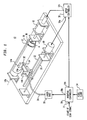
- the printer 10 comprises a drum 12 having a longitudinal axis 12a, a printhead 14 comprising first and second end flanges 14a and 14b, respectively, a drum motor 16, a translator motor 18, a lead screw translator 20, a support rail 22 for the printhead 14, a bundle 24 of optical fibers, a laser unit 26, a printer controller 28, a motor controller 30, a variable magnifying means 32 which preferably is a fixed conjugate focal point zoom lens mounted in the first flange 14a of the printhead 14, and a pixel clock 34.
- the drum 12 supports a receiver member 36 such as a sheet of paper onto which an image is transferred from each one of a set of dye donor members 38 on the receiver member 36. More particularly, each of the dye donors members 38 of the set of dye donor members is formed with a different dye or ink thereon such as yellow, magenta, or cyan.
- the dye donor members 38 of the set of dye donor members are sequentially placed in contact with the receiver member 36 to print a separate superimposed dye frame on the receiver member 36. When all of the dye donor members 38 of the set are used in sequential printing the superimposed dye frames, a complete image is formed on the receiver member 36.
- the printhead 14 is arranged to align the bundle 24 of optical fibers coming from the laser unit 26 into a predetermined array 24a of optical fibers disposed between the first and second flanges 14a and 14b, respectively.
- the fixed conjugate focal point zoom lens 32 is mounted in the first flange 14a between an end of the predetermined array 24a of optical fibers and the dye donor member 38 mounted on the receiver member 36 on the drum 12.
- the fixed conjugate focal point zoom lens 32 functions to provide an image of an instantaneous light pattern produced at the end of the predetermined array 24a of optical fibers onto the dye donor member 38 with a selective amount of magnification.
- Image information or data is brought to the printhead 14 from the laser unit 26 via the bundle 24 of optical fibers and the predetermined array 24a of optical fibers.
- the printer controller 28 is coupled at first and second outputs 28a and 28b to inputs of the laser unit 26 and the motor controller 30, respectively.
- the motor controller 30 is coupled at first and second outputs 30a and 30b to the drum motor
- the printhead 14 is moved parallel to the longitudinal axis 12a of the drum 12 by a lead screw translator 20 which is rotated by the translator motor 18 as the images are formed on the dye donor member 38. Concurrent therewith, the drum 12 is rotated in the direction designated by the arrow "A" by the drum motor 16.
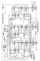
- the laser unit 26 comprises a plurality of N lasers 401 to 40 N , and a corresponding plurality of N laser drivers 421 to 42 N .
- Each of the N lasers 401 to 40 N is coupled to a separate corresponding one of the N laser drivers 421 to 42 N .
- only laser drivers 421, 422 and 42 N and the associated lasers 401, 402, and 40 N are shown.
- Each of the lasers drivers 421 to 42 N receive separately processed image data from the printer controller 28, and uses such data to modulate the light from the associated laser 40 as is well known in the art.
- the modulated light from the array of diode lasers 401 to 40 N is delivered via the bundle 24 and the predetermined array 24a of optical fibers, and the zoom lens 32 onto the dye donor member 38 (shown in FIG. 1) in order to print the image represented by the data on the receiver member 36 (shown in FIG. 1).
- the printer controller 28 comprises a Raster Image Source (RIS) 50, a parser 52, a plurality of N Laser Data Channel circuits 541 to 54 N (each Channel circuit being shown within a dashed line rectangle with only Channel Circuits 541, 542, and 54 N being shown), a first and a second bus 56 and 58, an address lead 60, a Start of Scan signal lead 77, and a Controlling Central Processing Unit (CPU) 79.
- RIS Raster Image Source
- the RIS 50 can be disposed remote from the printer controller 28 for supplying image data to the parser 52.
- the parser 52 comprises first and second inputs for receiving image data from the RIS 50 and each of the N Laser Data Channel Circuits 54 via second bus 58, respectively, and first and second outputs that provide image data and addresses, respectively, to each of the N Laser Data Channel Circuits 541 to 54 N via the respective first bus 56 and address lead 60.
- Each of the N Laser Data Channel Circuits 541 to 54 N comprises address compare means (ADDR. COMPARE) 70, first switching means (switch) 71, First-In-First-Out (FIFO) means 72, second switching means (SWITCH) 73, a Lookup Table 74, delay means (DELAY) 75, and an output circuit 76.
- the address compare means 70 receives addresses from the parser 52 via the address lead 60, outputs a first selective enabling signal to the first switching means 71 via a first output, and outputs a second selective enabling signal to the second switching means 73 via a second output.
- the first switching means 71 is responsive to the first selective enabling signal from the first output of the address compare means 70 to pass image data currently received on the first bus 56 to the FIFO 72.
- the FIFO 72 stores a plurality of bits of image data forming at least one line of image data, and outputs the oldest received bit of data stored therein to the Lookup table 74 when requested from the output circuit 76.
- a second output from the FIFO 72 provides an output signal indicating whether the FIFO 72 is full of data or not to the second switching means 73 for transmission via the second bus 58 to the second input of the parser 52 when enabled by an enabling signal from the second output of the address compare means 70.
- the Lookup Table 74 receives each bit of data outputted by the FIFO 72, and generates an output signal to the output circuit 76 based on such received data bit.
- Each of the Lookup Tables 74 in the plurality of N Laser Data Channel Circuits 541 to 54 N function to balance differences between the lasers 401 to 40 N in the laser unit 26. More particularly, it is expected that all pixels of the image data having the same data value will produce a same density of a printed pixel on the receiver member 36 (not shown) mounted on the drum 12 (shown in FIG. 1), and that there is some relationship (usually linear) between the possible data values.
- each of the lasers 401 to 40 N are capable of receiving each of the possible data values from the associated one of the Laser Data Channel Circuits 541 to 54 N , and are expected to mark the associated dot on the receiver member 36 with the correct density value for each of the possible data values.
- a first problem is that not all of the diode lasers 401 to 40 N have precisely the same characteristics as all of the other lasers. As a result, all of the diode lasers 401 to 40 N will not mark a dot on the receiver member 36 on the drum 12 with a same density value for a given input data value.
- the lasers 401 to 40 N are equalized by the use of the Lookup Tables 74 in the Laser Data Channel Circuits 541 to 54 N , respectively.
- a second problem is that there can be a nonlinear relationship between the input data values and the density values printed by such data values. This is caused by a plurality of different factors such as the characteristics of the lasers 401 to 40 N , the media (the dye donor member 38 and the receiver member 36), the optics, etc.
- each Lookup Table 74 maps out and linearizes such nonlinear relationships.
- the delay means 75 and the output circuit 76 are driven by a synchronous pixel clock 34 (shown in FIG. 1) that is phase-locked to the rotation of the drum 12 (shown in FIG. 1). This ensures a good swath-to-swath alignment in a fast scan direction corresponding to the rotation of the drum 12 as shown by the arrow designated "A" in FIG. 1. More particularly, it is to be understood that with a linear array of N diode lasers 401 to 40 N , all of the channels (pixels from the lasers 401 to 40 N ) may not be on a same perpendicular line in a slow scan direction parallel to the longitudinal axis 12a the drum 12. To compensate for this, the delay means 75 counts a programmed number of pixel clock cycles (pulses) after a start of scan signal is received on lead 77 as is explained hereinafter.
- a simple and easy technique is provided for changing dot density in dot per inch (DPI) and dot size in a multi-beam or multi-channel printing system (such as a multi-fiber array printing system).
- DPI dot per inch
- a screen dot is divided into a matrix of smaller microdots to achieve a gray scale in halftone printing.
- a screen dot is composed of an n-by-n (nxn) microdot matrix for providing n2 steps of gray levels.
- nxn n-by-n
- an 1800 microdot per inch (DPI) printer can be produced using 150 screen dots with each dot having a 12x12 microdot matrix, or 300 screen dots with each dot having a 6x6 microdot matrix.
- each microdot is further subdivided into an mxm matrix.
- the nxn microdot matrix for each screen dot becomes an (nxn) (mxm) sub-microdot matrix.
- the printing pixel density becomes (n) (m) (S), where S is the screen ruling density [e.g., having a range between 75 and 300 screen dots per inch (SDPI)].
- SDPI screen dots per inch
- 1 is capable of printing, for example, a set of eight distinctive microdot densities of 3600, 1800, 1200, 900, 720, 600, 450, and 300 microdots per inch (MDPI) using 1x1, 2x2, 3x3, 4x4, 5x5, 6x6, 8x8, and 12x12 sub-microdot matrixing, respectively.
- MDPI microdots per inch
- other printing microdot densities between the above-mentioned 3600, 1800, 1200, 900, 720, 600, 450, and 300 MDPI microdot densities are achieved using the fixed conjugate focal point zoom lens 32 (shown in FIGS. 1, 4 and 5).
- the fixed conjugate focal point zoom lens 32 is adjusted to magnify an 3600 MDPI printer 10 set-up to produce the desired 2400 MDPI dot density.
- the combination of sub-microdot matrixing and optical magnification or demagnification using a fixed conjugate focal point zoom lens 32 permits the printer 10 to cover a large number of dot and microdot sizes and screen dot densities in accordance with the present invention.
- the line spacing or written dot size has to be able to be changed.
- the optical magnification has to be changed in order to change the dot size or density. This requires a complicated optical system or the zoom lens 32 which are each generally found to have a limitation on the range of optical magnification change. Additionally, it is very difficult to cover a dot density ranging from 300 MDPI to over 3600 MDPI.
- the use of sub-microdot matrixing, as described hereinbefore overcomes this difficulty. More particularly, to change the dot density, the data is altered accordingly for each of the lines of the image.
- the image data has to repeat itself in both the slow and fast scan directions.
- the input data has to be rerouted to the grouping of sub-microdot matrixing.
- sub-microdot matrixing For example, if 2x2 sub-microdot matrixing is used, two adjacent lines are fed the same image data in the slow scan direction (along a longitudinal axis 12a of the drum 12), and the pixel clock 34 is halved so that each dot is twice as long in the fast scan direction (direction of rotation of the drum 12 in FIG. 1). If 3x3 sub-microdot matrixing is used, 3 adjacent lines are fed the same image data in the slow scan direction. In other words, the sub-microdot matrixing technique requires stretching (in the fast scan direction) and duplicating (in the slow scan direction) the data in two dimensions.
- the image data is supplied by the Raster Image Source (RIS) 50 as a serial stream, one line after another.
- the line direction of the image data supplied by the RIS 50 is aligned with the fast scan direction (arrow A in FIG. 1) of printer 10.
- the data stream from the RIS 50 is parsed by the parser 52 so that, as a general concept, one line of image data goes to one print channel (e.g., Laser Data Channel Circuit the next line of data to the next print channel (e.g., Laser Data Channel Circuit 542), etc.
- the FIFO 72 therein holds the data for a present line while other elements (not shown) in the parser 52 are being loaded with an additional line of data.
- the parser 52 is reprogrammed so that it sends the data to multiple print channels at the same time. More particularly, if the printer 10 is writing at it's maximum resolution (e.g., 3600 MDPI using 1x1 sub-microdot matrixing), then the parser 52 acts normally to send a first line of data to Laser Data Channel Circuit 541, a next line of data to the next subsequent Laser Data Channel Circuit 542, etc.
- maximum resolution e.g., 3600 MDPI using 1x1 sub-microdot matrixing
- the parser 52 sends a first line of data to the first and second Laser Data Channel Circuits 541and 542, respectively, a second line of data to the third and fourth Laser Data Channel Circuits 543 and 544, respectively, etc.
- the parser 52 still only sends each line of data once.
- the address compare means 70 of the first and second Laser Data Channel Circuits 541 and 542 are loaded with the same value (address) so that when the parser 52 transmits this address on line 60, both Channel Circuits 541 and 542 enable their first and second switching means 71 and 73.
- both Laser Data Channel Circuits 541 and 542 receive the data sent by the parser 52 on line 56, and both Laser Data Channel Circuits 541 and 542 send full flag signals to the parser 52 via bus 58 to throttle the transfer. If the resolution is set to 1200 MDPI (using 3x3 sub-microdot matrixing), then a first line of data is sent to the first, second, and third Laser Data Channel Circuits 541, 542, and 543, respectively, the second line of data is sent to the fourth, fifth, and sixth Laser Data Channel Circuits 544, 545, and 546, respectively, etc.
- the data is shifted out in the fast scan direction with reference to the pixel clock 34 which is phase-locked to the rotation of drum 12, or with reference to an open loop clock (not shown).
- the pixel clock 34 or the open loop clock
- the pixel clock 34 has a frequency of f0 when writing at a maximum resolution (e.g., 3600 MDPI).
- a maximum resolution e.g. 3600 MDPI.
- the Controlling CPU 79 functions to inform (a) the parser 52 of the number of effective channels to be used based on a selected matrix (e.g., 1x1, 2x2, etc.) via lead 79a, (b) the address compare means 70 of the channel address for each of the Laser Data Channel Circuits 541 to 54 N based on the selected matrix via bus 79b, and (c) the delay means 75 of the delay to be used for each of the Laser Data Channel Circuits 541 to 54 N based on the magnification of the zoom lens 32 via bus 79c.
- a selected matrix e.g., 1x1, 2x2, etc.
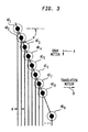
- FIG. 3 there is shown an arrangement of a plurality of N lasers 401 to 40 N , of which lasers 401, 402, 403, 404, 405, 406, 407, 408, and 40 N are shown, for purposes of explanation of the delay circuits 75 and output circuits 76 of FIG. 2.
- the arrangement of present FIG. 3 and its description are extensively disclosed in copending U.S. Patent Application Serial No. 749,037 (T. A. Mackin et al), filed on August 23, 1991, where the present FIG. 3 is shown in the copending patent application as FIG. 4.
- the following description of present FIG. 3 is taken from a pertinent portion of the description provided in the copending application.
- the plurality of lasers 401 to 40 N are aligned and equally spaced to produce a correspondingly aligned and predetermined spaced set of laser light beams on the dye donor member 38 (shown in FIG. 1).
- the line of lasers 401 to 40 N are oriented at a predetermined acute angle ⁇ to the width of the receiver member 36 mounted on drum 12 in FIG. 1 corresponding to a line perpendicular to the direction of rotation A of the drum 12. More particularly, due to the smallness of the micropixels that are being written at 1800 MDPI (0.000556 inch/micropixel), a conventional printhead that provides light beams oriented parallel to the width of the receiver member 36 on the drum 12 cannot be built to provide the close micropixel spacing needed for printing.
- the horizontal distance "d" between lasers 401 to 40 N along the direction of translation motion shown by the arrow B can be made as small as necessary.
- the horizontal spacing "d" between adjacent lasers 40 represents the micropixel density of the image being printed on the receiver member 36 mounted on the drum 12.
- the number "N" of lasers 40 that are used in the laser unit 26 is determined by economies of scale only.
- the laser printer 10 will work whether there are two or two hundred lasers 40 for any size image. The trade off is the cost of the extra elements versus the speed at which the thermal printer 10 can print. Factors which make such determination are, for example, the micropixel size, the diameter of the drum 12, and the ability of the lasers 40 to focus their light beams onto the dye donor member 38 on the drum 12 (shown in FIG. 1).
- the laser printer 10 In order to print dots (micropixels) at, for example, 1800 MDPI, to create 4-color images on a receiver member 36, the laser printer 10 must maintain, for example, a ⁇ 1/8 micropixel resolution. By providing a ⁇ 1/8 micropixel resolution (R) in a 4-color image, the error cannot be detected by the human eye or by magnifications normally used in the graphic arts field (e.g., magnifications of 7x-20x). The laser printer 10 controls micropixel resolution to this tolerance by close synchronization of the position of the drum 16 and the pixel timing pulses from the pixel clock 30.
- the drum 12 is rotated at a continuous speed in the direction of the arrow A shown in FIGS. 1 and 3. Simultaneously therewith, the printhead 14 including the light beams from the plurality of lasers 400 to 40 N is translated at a slower speed across the drum 12 in the direction shown by arrow B of FIG. 3.
- Each of the plurality of laser 401 to 40 N associated with the laser printhead 14 writes a separate column of micropixels during each revolution of the drum 12.
- the image is written in a helical form because the printhead 14 is continuously translating (moving) in the direction of the arrow B as the drum 12 rotates in the direction of arrow A. Therefore, by aligning the plurality of lasers 401 to 40 N (and their light beams) at an acute angle ⁇ as shown in FIG. 3, N columns of the dye frame image are concurrently written during each revolution of the drum 12.
- the lasers 401 to 40 N are timed in a sequence that causes corresponding micropixels of each column to be substantially aligned across the width of the receiver member 36 on the drum 12. In this manner, N micropixels of each line of a dye frame image are written onto the receiver member 36 during each rotation of the drum 12. More particularly, in FIG. 3, when the first row of a dye frame image is started, the first laser 401 is energized (fired), and the drum 12 is moved a predetermined distance in direction of arrow A before the second laser 402 is fired to place the two micropixels next to each other with the proper spacing.
- the delay between the firing of the first laser 401 and the second laser 402 takes a predetermined plurality of pulses of the pixel clock 34.
- Such delay can be determined by those skilled in the art knowing various laser printer 10 factors such as the circumference of the drum 12, the rotational speed of the drum 12, the spacing of the light beams from the lasers 401 to 40 N from the printhead 14, and the angle ⁇ at which the light beams from the printhead 14 are disposed relative to a line perpendicular to the direction of rotation of the drum 12.
- the number (N) of lasers 40 does not effect the delay values.
- the laser 401 is fired sequentially at predetermined intervals synchronized to the rotational speed of the drum 12. More particularly, the laser 401 is fired every time the drum 12 moves a predetermined distance corresponding to the distance between each of the rows of the dye frame image. After the first laser 401 is fired for each row of the dye frame image, the remaining lasers 402 to 40 N are fired in the same timed sequence as described above for printing the first row of the dye frame image. In this manner, the lasers 401 to 40 N are energized for printing the N columns of the rows of a dye frame image during each rotation of the drum 12.
- next sequential plurality of N columns of the rows of the dye frame image, in the direction of translation motion of the printhead 14, are printed. These next sequential plurality of N columns are timed to be printed next to the corresponding rows printed during the prior revolutions of the drum 12, until the entire dye frame image is completed.
- the delay circuit 75 in each of the plurality of N Laser Data Channel Circuits 541 to 54 N is provided to compensate for such off-perpendicular alignment. More particularly, the delay circuit 75 counts a programmed number of cycles from the pixel clock 34 after a start of scan signal is received on the lead 77 before enabling the output circuit 76 to start shifting out data from the FIFO 72 via the lookup table 74.
- each channel has a unique value programmed into its delay circuit 75.
- Synchronous output enable pulses from the delay circuit 75 are usually some multiple of the clock rate of the pixel clock 34. This allows the delay circuit 75 to better align the output signals to the laser unit 26 from the Laser Data Channel Circuits 541 to 54 N .
- N channels 54 decreases the resolution in the line scan direction (slow scan perpendicular to the rotation of drum 12). A corresponding change is required in the pixel scan direction (fast scan direction in the rotational direction of drum 12) as well. This is accomplished by changing the number of synchronous clock pulses per revolution of the drum 12, and is accomplished by altering parameters in phase-lock circuitry (not shown) within the pixel clock 34.
- FIG. 2 An exemplary arrangement for the pixel clock 34 is shown in FIG. 2 of the hereinabove mentioned copending U.S. Patent application Serial No. 749,037 which is incorporated herein by reference.
- the phase-lock circuitry of the pixel clock 34 is designed to give "m" synchronous clock pulses per revolution of the drum 12 when printing at a maximum resolution (e.g., 3600 MDPI) to provide a predetermined pixel size. If the parameters of the phase-lock circuitry are changed to obtain only m/2 clock pulses per revolution, then each pixel is twice as long in the fast scan direction. This is a desired result for printing at one-half of the maximum resolution. The same logic applies for printing at all other resolutions. Therefore, the duplication in the fast scan direction does not require a creation of more data. Rather, duplication in the fast scan direction is accomplished by making the available data last longer.
- a maximum resolution e.g. 3600 MDPI
- the zoom lens 32 comprises a first set of lenses (shown under the bracket 80), a second set of lenses (shown within a dashed line rectangle 81), a third set of lenses (shown under the bracket 82), a first end 84 for receiving light rays from a first conjugate plane 85, a second end 86 for focusing the light rays passing through the zoom lens 32 onto a second conjugate plane 87, and a longitudinal axis 88.
- the first set of lenses 80 comprises a planar/convex lens 90 disposed adjacent the first end 84 of the zoom lens 32, and a concave/convex lens 91 for receiving light rays refracted by the lens 90.
- the concave/convex lens 91 is formed of a first concave/planar lens 91a and a second planar/convex lens 91b which have their planar ends abutting each other.
- the concave end of the lens 91a is disposed in a fixed relationship to the convex end of the lens 90.
- the first set of lenses 80 are disposed in a fixed relationship to the first end 84 of the zoom lens 32.
- the second set of lenses 81 is movable along the longitudinal axis 88 of the zoom lens 32 between the first set of lenses 80 and the third set of lenses 82.
- the second set of lenses 81 comprises a concave/convex lens 92 for receiving the light rays refracted by the first set of lenses 80 at its concave surface, and a concave/planar lens 93 which is disposed to receive the light refracted by the lens 93 at its concave surface and has a fixed relationship to the lens 93.
- the second set of lenses 81 is positioned near the first set of lenses 80 to provide a predetermined magnification (e.g., a magnification of 1) for the zoom lens 32.
- a predetermined magnification e.g., a magnification of 1
- the third set of lenses 82 comprises a convex/convex lens 94 for receiving light rays from the second set of lenses 81, a convex/concave lens 95 for receiving the light rays refracted by the lens 94, and a convex/concave lens 96 for receiving the light rays refracted by the lens 95 and focussing the light rays leaving the lens 96 onto the second conjugate plane 87.
- the convex/concave lens 95 comprises a first convex/convex lens 95a which abuts a second concave/concave lens 95b.
- the third set of lenses 82 is disposed in a fixed relationship to the second end 86 of the zoom lens 32, and each of the lenses 94, 95, and 96 are disposed in a fixed relationship to each other.
- first conjugate plane 85 represents the end of the optical fiber array 24a in the printhead 14 of FIG. 1 adjacent the first flange 14a
- second conjugate plane 87 represent the dye donor member 38 on the drum 12.
- FIG. 5 there is shown a side view of the lenses of the exemplary zoom lens 32 of FIG. 4 used in the laser printer of FIG. 1 to provide a second predetermined magnification.
- the lens 32 shown in FIG. 5 has the same internal lens configuration and number designations as shown for the zoom lens 32 in FIG. 4.
- the second section 81 is moved along the longitudinal axis 88 to adjacent the third set of lenses 82.
- the magnification of the zoom lens 32 from a minimum magnification of, for example, 1 times (shown in FIG. 4) to a maximum magnification of, for example, 2 times (shown in FIG.
- the dot spacing (density in microdots per inch) is varied at the second conjugate plane 87. Therefore, if the zoom lens 32 has a maximum power (magnification) of 2, any dot density from 300 MDPI to 3600 MDPI can be achieved using the combination of sub-microdot matrixing and variable zoom lens 32 magnifications.
- a dot density of 2400 MDPI microdot matrixing is achieved in accordance with the present invention by setting the printer controller 28 to provide 3600 MDPI microdot matrixing and magnifying the 3600 MDPI to 2400 MDPI using the zoom lens set at a magnification of 1.5.
- FIGS. 6A and 6B there are shown images 1001 to 1008 of only the lasers 401 to 408, respectively, of FIG. 3 at the dye donor member 38 of the exemplary laser printer 10 of FIG. 1 for magnifications of 1 and 1.5, respectively, provided by the zoom lens 32.
- a line spacing P and a radius R are changed to a line spacing of P' and a radius of R' (shown in FIG. 6B) by a factor of 1.5.
- the printer 10 can print halftone images which require very high pixel density from 1000 to 3600 DPI and continuous tone images which require a relatively low pixel density typically from 150 to 600 DPI. It is to be understood that the magnification setting of the zoom lens 32 is preferably performed automatically when a printer operator inputs a MDPI value between 300 and 3600 MDPI.
- the laser unit and the optical fiber cable and array can be formed on as part of the printhead 14, with the printer controller 28 supplying the processed image data to the laser unit via an electrical cable (not shown).
Landscapes
- Engineering & Computer Science (AREA)
- Multimedia (AREA)
- Signal Processing (AREA)
- Fax Reproducing Arrangements (AREA)
- Laser Beam Printer (AREA)
- Dot-Matrix Printers And Others (AREA)
- Electronic Switches (AREA)
- Image Processing (AREA)
- Facsimile Image Signal Circuits (AREA)
Applications Claiming Priority (2)
| Application Number | Priority Date | Filing Date | Title |
|---|---|---|---|
| US07/892,884 US5754218A (en) | 1992-06-03 | 1992-06-03 | Variable dot density printing system using sub-microdot matrixing and a zoom lens |
| US892884 | 1997-07-15 |
Publications (2)
| Publication Number | Publication Date |
|---|---|
| EP0573370A1 true EP0573370A1 (fr) | 1993-12-08 |
| EP0573370B1 EP0573370B1 (fr) | 2000-01-12 |
Family
ID=25400661
Family Applications (1)
| Application Number | Title | Priority Date | Filing Date |
|---|---|---|---|
| EP93420218A Expired - Lifetime EP0573370B1 (fr) | 1992-06-03 | 1993-05-28 | Système d'imprimante des points à densité variable avec utilisation des matrices de sous-micropoint et d'un objectif zoom |
Country Status (4)
| Country | Link |
|---|---|
| US (1) | US5754218A (fr) |
| EP (1) | EP0573370B1 (fr) |
| JP (1) | JP3725905B2 (fr) |
| DE (1) | DE69327549T2 (fr) |
Families Citing this family (15)
| Publication number | Priority date | Publication date | Assignee | Title |
|---|---|---|---|---|
| JPH10123413A (ja) * | 1996-10-21 | 1998-05-15 | Dainippon Screen Mfg Co Ltd | 画像記録用レンズ及び結像装置 |
| JPH10119348A (ja) * | 1996-10-22 | 1998-05-12 | Fuji Photo Film Co Ltd | 画像記録装置 |
| EP1552943B1 (fr) | 1997-03-26 | 2012-06-06 | Toray Industries, Inc. | Dispositif d'imagerie, procédé d'imagerie et dispositif d'impression |
| JP3889484B2 (ja) * | 1997-07-23 | 2007-03-07 | 株式会社沖データ | プリンタ装置 |
| US5949523A (en) * | 1997-09-16 | 1999-09-07 | Lifetouch Portrait Studios, Inc. | High speed package printer |
| US6185313B1 (en) * | 1998-07-30 | 2001-02-06 | Eastman Kodak Company | Method and apparatus for printing copy restrictive documents having individual keycodes |
| US6604806B1 (en) | 1999-10-20 | 2003-08-12 | Canon Kabushiki Kaisha | High resolution printing |
| US6352330B1 (en) | 2000-03-01 | 2002-03-05 | Eastman Kodak Company | Ink jet plate maker and proofer apparatus and method |
| US6313433B1 (en) | 2000-04-03 | 2001-11-06 | Universal Laser Systems, Inc | Laser material processing system with multiple laser sources apparatus and method |
| US6816183B2 (en) * | 2000-11-04 | 2004-11-09 | Fuji Photo Film Co., Ltd. | Recording medium package, feed cassette and recording apparatus using the same |
| US6753898B2 (en) | 2001-03-29 | 2004-06-22 | Masanori Kubota | Method and apparatus for high speed digitized exposure |
| US7804607B2 (en) * | 2001-09-14 | 2010-09-28 | Canon Kabushiki Kaisha | Group printer for multiple member printers |
| JP4373731B2 (ja) * | 2003-07-22 | 2009-11-25 | 富士フイルム株式会社 | 描画装置及び描画方法 |
| US7852510B2 (en) * | 2005-04-28 | 2010-12-14 | Xerox Corporation | Systems and methods for setting configuring rendering parameters for high-speed rendering devices |
| US20220258510A1 (en) * | 2021-02-16 | 2022-08-18 | Primera Technology, Inc. | Laser imaging printer and die cutter assembly |
Citations (4)
| Publication number | Priority date | Publication date | Assignee | Title |
|---|---|---|---|---|
| GB2156624A (en) * | 1984-02-15 | 1985-10-09 | Dainippon Screen Mfg | A scanning image reproduction system including a plurality of modulated laser beams |
| US4740844A (en) * | 1985-04-19 | 1988-04-26 | Ricoh Company, Ltd. | Method of changing magnification of image |
| US4780768A (en) * | 1985-09-06 | 1988-10-25 | Dainippon Screen Mfg. Co., Ltd. | Halftone image recording method and apparatus |
| EP0529539A2 (fr) * | 1991-08-23 | 1993-03-03 | Eastman Kodak Company | Imprimante thermique à haute résolution |
Family Cites Families (12)
| Publication number | Priority date | Publication date | Assignee | Title |
|---|---|---|---|---|
| US3983319A (en) * | 1973-11-12 | 1976-09-28 | Printing Developments, Inc. | Electronic screening for image reproduction |
| US4189752A (en) * | 1973-11-12 | 1980-02-19 | Printing Developments, Inc. | Electronic screening with galvanometer recorders |
| US3988742A (en) * | 1975-04-28 | 1976-10-26 | Mcdonnell Douglas Corporation | Recorder using light emitting diodes |
| US4296197A (en) * | 1977-06-03 | 1981-10-20 | Innovative Photograhic Enterprises, Inc. | Halftone printing system |
| JPS5714058A (en) * | 1980-06-28 | 1982-01-25 | Ricoh Co Ltd | Printer |
| JPS5978353A (ja) * | 1982-10-28 | 1984-05-07 | Dainippon Screen Mfg Co Ltd | 網目版画像記録装置における網点形成方法 |
| ATE19451T1 (de) * | 1982-11-06 | 1986-05-15 | Hell Rudolf Dr Ing Gmbh | Verfahren zur einstellung und ueberwachung eines belichtungsflecks. |
| US4547814A (en) * | 1982-12-06 | 1985-10-15 | Dainippon Screen Seizo Kabushiki Kaisha | Method of recording a halftone picture electronically |
| US4651287A (en) * | 1984-06-14 | 1987-03-17 | Tsao Sherman H | Digital image processing algorithm for output devices with discrete halftone gray scale capability |
| FR2587572B1 (fr) * | 1985-03-20 | 1994-02-18 | Canon Kk | Appareil et procede de traitement d'images |
| US4949105A (en) * | 1989-08-16 | 1990-08-14 | Eastman Kodak Company | Process control patch generator |
| US5164742A (en) * | 1989-12-18 | 1992-11-17 | Eastman Kodak Company | Thermal printer |
-
1992
- 1992-06-03 US US07/892,884 patent/US5754218A/en not_active Expired - Fee Related
-
1993
- 1993-05-28 EP EP93420218A patent/EP0573370B1/fr not_active Expired - Lifetime
- 1993-05-28 DE DE69327549T patent/DE69327549T2/de not_active Expired - Fee Related
- 1993-06-03 JP JP13309293A patent/JP3725905B2/ja not_active Expired - Fee Related
Patent Citations (4)
| Publication number | Priority date | Publication date | Assignee | Title |
|---|---|---|---|---|
| GB2156624A (en) * | 1984-02-15 | 1985-10-09 | Dainippon Screen Mfg | A scanning image reproduction system including a plurality of modulated laser beams |
| US4740844A (en) * | 1985-04-19 | 1988-04-26 | Ricoh Company, Ltd. | Method of changing magnification of image |
| US4780768A (en) * | 1985-09-06 | 1988-10-25 | Dainippon Screen Mfg. Co., Ltd. | Halftone image recording method and apparatus |
| EP0529539A2 (fr) * | 1991-08-23 | 1993-03-03 | Eastman Kodak Company | Imprimante thermique à haute résolution |
Also Published As
| Publication number | Publication date |
|---|---|
| JPH06152939A (ja) | 1994-05-31 |
| EP0573370B1 (fr) | 2000-01-12 |
| DE69327549D1 (de) | 2000-02-17 |
| US5754218A (en) | 1998-05-19 |
| DE69327549T2 (de) | 2000-07-27 |
| JP3725905B2 (ja) | 2005-12-14 |
Similar Documents
| Publication | Publication Date | Title |
|---|---|---|
| EP0573370B1 (fr) | Système d'imprimante des points à densité variable avec utilisation des matrices de sous-micropoint et d'un objectif zoom | |
| US7206099B2 (en) | Media/screen look-up-table for color consistency | |
| US4626901A (en) | Image processing apparatus using multiple dither matrices | |
| JPH0463584B2 (fr) | ||
| EP0605131B1 (fr) | Méthode et appareil pour éliminer la distortion par illumination surbalayée pour imprimantes optiques ou similaires ayant des milieux d'enregistrement photosensibles à grand contraste et à haute adressabilité | |
| US7231096B2 (en) | Screening method for overlapping sub-images | |
| US5767887A (en) | System for plotting graphic Images | |
| US4920502A (en) | Image processing apparatus which selectably outputs image information | |
| US4893195A (en) | Image processing apparatus capable of eliminating moire pattern | |
| US4713701A (en) | Picture producing apparatus using multiple dot forming units and recording materials of different concentrations | |
| US6816269B1 (en) | Method and apparatus for electronic registration in a binary image path | |
| US4905095A (en) | Image processing apparatus | |
| GB2215554A (en) | Image reader and printer | |
| JPH05300348A (ja) | 校正印刷機 | |
| US6268929B1 (en) | Data processing device for simultaneously reading out plural lines of image and a method therefor | |
| EP0879147A1 (fr) | Systeme d'imagerie a haute resolution et procede d'imagerie utilisant ce systeme | |
| EP0947950B1 (fr) | Procédé et appareil pour entrelacer des lignes de balayage à trame dans un dispositif d'imagerie laser à faisceaux multiples | |
| JP3620580B2 (ja) | ライン露光式画像形成装置 | |
| US4521814A (en) | Method and apparatus for simultaneously outputting a graphic signal and an alphanumeric signal by using an image reproducing system | |
| US4958239A (en) | Method of gradation and selection of micro picture elements therefor in a picture display | |
| US6101018A (en) | Light beam scanning optical apparatus | |
| EP0664522B1 (fr) | Contrôle d'exposition xérographique à plusieurs niveaux par balayage à faisceaux multiples | |
| EP0999694B1 (fr) | Procédé et système de tramage pour sous-images chevauchantes | |
| JP2516460B2 (ja) | カラ―画像記録装置 | |
| JPH0568911B2 (fr) |
Legal Events
| Date | Code | Title | Description |
|---|---|---|---|
| PUAI | Public reference made under article 153(3) epc to a published international application that has entered the european phase |
Free format text: ORIGINAL CODE: 0009012 |
|
| AK | Designated contracting states |
Kind code of ref document: A1 Designated state(s): DE FR GB |
|
| 17P | Request for examination filed |
Effective date: 19940519 |
|
| 17Q | First examination report despatched |
Effective date: 19960320 |
|
| GRAG | Despatch of communication of intention to grant |
Free format text: ORIGINAL CODE: EPIDOS AGRA |
|
| GRAG | Despatch of communication of intention to grant |
Free format text: ORIGINAL CODE: EPIDOS AGRA |
|
| GRAH | Despatch of communication of intention to grant a patent |
Free format text: ORIGINAL CODE: EPIDOS IGRA |
|
| GRAH | Despatch of communication of intention to grant a patent |
Free format text: ORIGINAL CODE: EPIDOS IGRA |
|
| GRAA | (expected) grant |
Free format text: ORIGINAL CODE: 0009210 |
|
| AK | Designated contracting states |
Kind code of ref document: B1 Designated state(s): DE FR GB |
|
| REF | Corresponds to: |
Ref document number: 69327549 Country of ref document: DE Date of ref document: 20000217 |
|
| PGFP | Annual fee paid to national office [announced via postgrant information from national office to epo] |
Ref country code: GB Payment date: 20000404 Year of fee payment: 8 |
|
| PGFP | Annual fee paid to national office [announced via postgrant information from national office to epo] |
Ref country code: FR Payment date: 20000504 Year of fee payment: 8 |
|
| ET | Fr: translation filed | ||
| PGFP | Annual fee paid to national office [announced via postgrant information from national office to epo] |
Ref country code: DE Payment date: 20000531 Year of fee payment: 8 |
|
| PLBE | No opposition filed within time limit |
Free format text: ORIGINAL CODE: 0009261 |
|
| STAA | Information on the status of an ep patent application or granted ep patent |
Free format text: STATUS: NO OPPOSITION FILED WITHIN TIME LIMIT |
|
| 26N | No opposition filed | ||
| PG25 | Lapsed in a contracting state [announced via postgrant information from national office to epo] |
Ref country code: GB Free format text: LAPSE BECAUSE OF NON-PAYMENT OF DUE FEES Effective date: 20010528 |
|
| GBPC | Gb: european patent ceased through non-payment of renewal fee |
Effective date: 20010528 |
|
| PG25 | Lapsed in a contracting state [announced via postgrant information from national office to epo] |
Ref country code: FR Free format text: LAPSE BECAUSE OF NON-PAYMENT OF DUE FEES Effective date: 20020131 |
|
| PG25 | Lapsed in a contracting state [announced via postgrant information from national office to epo] |
Ref country code: DE Free format text: LAPSE BECAUSE OF NON-PAYMENT OF DUE FEES Effective date: 20020301 |