EP0573520B1 - Composant optoelectronique - Google Patents
Composant optoelectronique Download PDFInfo
- Publication number
- EP0573520B1 EP0573520B1 EP92905858A EP92905858A EP0573520B1 EP 0573520 B1 EP0573520 B1 EP 0573520B1 EP 92905858 A EP92905858 A EP 92905858A EP 92905858 A EP92905858 A EP 92905858A EP 0573520 B1 EP0573520 B1 EP 0573520B1
- Authority
- EP
- European Patent Office
- Prior art keywords
- light
- optoelectronic component
- building block
- component according
- housing
- Prior art date
- Legal status (The legal status is an assumption and is not a legal conclusion. Google has not performed a legal analysis and makes no representation as to the accuracy of the status listed.)
- Expired - Lifetime
Links
Images
Classifications
-
- H—ELECTRICITY
- H10—SEMICONDUCTOR DEVICES; ELECTRIC SOLID-STATE DEVICES NOT OTHERWISE PROVIDED FOR
- H10W—GENERIC PACKAGES, INTERCONNECTIONS, CONNECTORS OR OTHER CONSTRUCTIONAL DETAILS OF DEVICES COVERED BY CLASS H10
- H10W90/00—Package configurations
-
- H—ELECTRICITY
- H10—SEMICONDUCTOR DEVICES; ELECTRIC SOLID-STATE DEVICES NOT OTHERWISE PROVIDED FOR
- H10F—INORGANIC SEMICONDUCTOR DEVICES SENSITIVE TO INFRARED RADIATION, LIGHT, ELECTROMAGNETIC RADIATION OF SHORTER WAVELENGTH OR CORPUSCULAR RADIATION
- H10F55/00—Radiation-sensitive semiconductor devices covered by groups H10F10/00, H10F19/00 or H10F30/00 being structurally associated with electric light sources and electrically or optically coupled thereto
- H10F55/20—Radiation-sensitive semiconductor devices covered by groups H10F10/00, H10F19/00 or H10F30/00 being structurally associated with electric light sources and electrically or optically coupled thereto wherein the electric light source controls the radiation-sensitive semiconductor devices, e.g. optocouplers
- H10F55/25—Radiation-sensitive semiconductor devices covered by groups H10F10/00, H10F19/00 or H10F30/00 being structurally associated with electric light sources and electrically or optically coupled thereto wherein the electric light source controls the radiation-sensitive semiconductor devices, e.g. optocouplers wherein the radiation-sensitive devices and the electric light source are all semiconductor devices
-
- H—ELECTRICITY
- H10—SEMICONDUCTOR DEVICES; ELECTRIC SOLID-STATE DEVICES NOT OTHERWISE PROVIDED FOR
- H10F—INORGANIC SEMICONDUCTOR DEVICES SENSITIVE TO INFRARED RADIATION, LIGHT, ELECTROMAGNETIC RADIATION OF SHORTER WAVELENGTH OR CORPUSCULAR RADIATION
- H10F77/00—Constructional details of devices covered by this subclass
- H10F77/40—Optical elements or arrangements
- H10F77/407—Optical elements or arrangements indirectly associated with the devices
-
- H—ELECTRICITY
- H10—SEMICONDUCTOR DEVICES; ELECTRIC SOLID-STATE DEVICES NOT OTHERWISE PROVIDED FOR
- H10F—INORGANIC SEMICONDUCTOR DEVICES SENSITIVE TO INFRARED RADIATION, LIGHT, ELECTROMAGNETIC RADIATION OF SHORTER WAVELENGTH OR CORPUSCULAR RADIATION
- H10F77/00—Constructional details of devices covered by this subclass
- H10F77/50—Encapsulations or containers
-
- H—ELECTRICITY
- H10—SEMICONDUCTOR DEVICES; ELECTRIC SOLID-STATE DEVICES NOT OTHERWISE PROVIDED FOR
- H10H—INORGANIC LIGHT-EMITTING SEMICONDUCTOR DEVICES HAVING POTENTIAL BARRIERS
- H10H20/00—Individual inorganic light-emitting semiconductor devices having potential barriers, e.g. light-emitting diodes [LED]
- H10H20/80—Constructional details
- H10H20/85—Packages
- H10H20/8506—Containers
-
- H—ELECTRICITY
- H10—SEMICONDUCTOR DEVICES; ELECTRIC SOLID-STATE DEVICES NOT OTHERWISE PROVIDED FOR
- H10H—INORGANIC LIGHT-EMITTING SEMICONDUCTOR DEVICES HAVING POTENTIAL BARRIERS
- H10H20/00—Individual inorganic light-emitting semiconductor devices having potential barriers, e.g. light-emitting diodes [LED]
- H10H20/80—Constructional details
- H10H20/85—Packages
- H10H20/855—Optical field-shaping means, e.g. lenses
-
- H—ELECTRICITY
- H10—SEMICONDUCTOR DEVICES; ELECTRIC SOLID-STATE DEVICES NOT OTHERWISE PROVIDED FOR
- H10H—INORGANIC LIGHT-EMITTING SEMICONDUCTOR DEVICES HAVING POTENTIAL BARRIERS
- H10H20/00—Individual inorganic light-emitting semiconductor devices having potential barriers, e.g. light-emitting diodes [LED]
- H10H20/80—Constructional details
- H10H20/85—Packages
- H10H20/855—Optical field-shaping means, e.g. lenses
- H10H20/856—Reflecting means
Definitions
- the present invention relates to an optoelectronic component comprising a number of light-emitting and/or light-receiving semiconductor elements which are arranged on a base, as well as a housing which surrounds the base and together with this forms a closed casing for the semiconductor elements.
- a commonly used such casing comprises a round base, on one plane surface of which one or several optoelectronic semiconductor elements is or are arranged. After mounting of the semiconductor element or the semiconductor elements on the base, a similarly round housing is fitted over the base and connected thereto, for example by welding the joint. In connection with casings of this kind, there must be a certain play between the housing and the base. This makes it possible for the position of the housing relative to the base to be changed in an uncontrolled manner between the fitting of the housing on the base and the subsequent welding of the housing to the base.
- a rotation of the housing relative to the base after the fitting of the housing in the desired position, means that the function of the component is reduced or that the component is rendered incapable of functioning.
- components which, in principle, are rotationally symmetrical with one single centrally arranged semiconductor element and with one centrally arranged light opening or lens in the housing an accurate centering of the housing in relation to the base is often required. Because of a play between the housing and the base, a displacement of the position of the housing relative to the base may easily occur between the fitting of the housing and the subsequent welding to the base. This makes it impossible to attain the desired accurate centering.
- the manufacture of components of the kind described above has either required extra time- and cost-demanding manufacturing stages to ensure the desired relative position between the housing and the base, or the manufacture has resulted in a high percentage of defective components.
- Certain optoelectronic components comprise a light-emitting semiconductor element for emitting light to the surroundings as well as a light-receiving element for receiving light from the surroundings.
- a light-emitting semiconductor element for emitting light to the surroundings
- a light-receiving element for receiving light from the surroundings.
- optocouplers comprise a light-emitting and a light-receiving semiconductor element, between which signals are transmitted optically to avoid a galvanic connection between the circuits to which the two semiconductor elements are connected.
- a light-emitting and a light-receiving semiconductor element between which signals are transmitted optically to avoid a galvanic connection between the circuits to which the two semiconductor elements are connected.
- such members tend to increase the complexity and the manufacturing cost of a component, and it is desirable that the desired control of the radiation can be made in the simplest and economically most favourable way.
- Certain other types of optoelectronic components are intended for bidirectional signal transmission, for example through an optical fibre.
- a typical such component comprises a light-emitting semiconductor element and a light-receiving semiconductor element, which respectively emit and receive optical radiation through a common opening or lens in the housing.
- this type of components there are problems in obtaining the required screening of direct radiation between the semiconductor elements as well as in causing emitted light from the light-emitting semiconductor element to be passed out through the common opening or lens in the desired direction and with a high efficiency while at the same time light falling against the component is passed with good efficiency to the light-receiving semiconductor element. Attaining these objectives at the same time has proved to be difficult and to give rise to complicated and hence uneconomical solutions.
- the invention aims to provide a component of the kind described in the introduction, in which, in a simple manner, an efficient locking of the housing in the desired position between the fitting of the housing onto the base and the welding of the housing to the base, performed in a subsequent manufacturing stage, is obtained.
- the invention also aims to provide a component in which the desired screening or control of the radiation between semiconductor elements present in the housing can be achieved in a simple manner.
- the invention aims to provide a component in which the control of the light flow between one or more openings or lenses in the housing and the semiconductor elements arranged in the housing can be achieved in a simple manner.
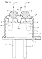
- Figure 1a shows a section through a so-called reflection detector according to the invention.
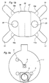
- Figure 1b shows the shape of the building block which is included in the component according to Figure 1a
- Figure 1c shows a side view of the building block
- figure 1d shows the building block seen in a direction which coincides with the symmetry axis of the component.
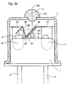
- Figure 2 shows a component for bidirectional (duplex) signal transmission
- Figure 2a showing the surface of the base with the semiconductor elements placed thereon
- Figure 2b showing a section through the component.
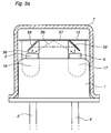
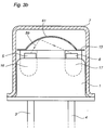
- Figure 3a and Figure 3b show two alternative embodiments of an optocoupler according to the invention.
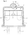
- Figure 4 shows a component according to the invention, which comprises a light emitting diode (LED).
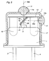
- Figure 5 shows a component according to the invention with an LED adapted to emit light through two separate exit openings in the housing.
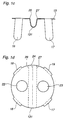
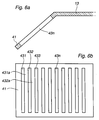
- Figure 6 shows how the partially reflecting members, used in Figure 2b and Figure 5, can be achieved in an alternative way by openings in the building block included in the component.
- LED light emitting diode
- Figure 1a shows a so-called reflection detector according to the invention. It comprises a light-emitting semiconductor 5, for example an LED or a laser diode, as well as a light-detecting member 6, for example a photodiode or a phototransistor, for detection of such emitted radiation which is reflected from an object located outside the component.
- the semiconductor elements are mounted on the plane surface of a rotationally symmetrical base 1, which is provided with a flange 2 and leads 3 and 4.
- a housing 7, also of rotationally symmetrical shape, is fitted on the base and forms together with this a closed casing for the semiconductor elements. The housing is welded to the flange 2 of the base.
- the housing is provided with openings 11a, 12a, which are provided with lenses 11, 12 for focussing the radiation.
- a central light ray from the element 5 is designated 9 in the figure and a central light ray received by the element 6 is designated 10.
- light in this application is meant optical radiation, both within and outside the visible wavelength band.
- a building block 13 is arranged in the component.
- the building block has four legs, of which the legs 16 and 17 are shown in Figure la, as well as a screen portion 131 for screening the direct radiation.
- the building block 13 is made of a thin metal plate, for example a copper beryllium alloy, and has the thickness 50 »m.
- the plate is etched out with the shape shown in Figure 1b.
- the building block has the four. legs 16, 17, 18, 19 and two openings 22, 23 to let through light to and from the two semiconductor elements, respectively.
- 24 designates the symmetry line of the building block, which will coincide with the centre of the screen portion 131.
- 26 and 27 designate the edges of the prospective screen portion.
- the plate shown in Figure 1b After manufacture of the plate shown in Figure 1b, this is pressed into the desired shape in a suitable fixture (Figs. 1c and 1d).
- the pressing is performed such that the four legs of the element are folded down into a right angle, or to a near right angle in relation to the plane main portion of the element (at the dashed lines 16a, 17a, 18a, 19a in Fig. 1b), and further such that the central part of the plate is bent down and forms the screen portion 131.
- the building block may suitably be hardened and then becomes resilient.
- the semiconductor elements 5, 6 When mounting the optoelectronic component according to the invention, the semiconductor elements 5, 6 are first applied to the base 1, whereafter the building block 13 is fitted on the base so far that the screen portion 131 will make contact with the base.
- the housing 7 is applied on the base and adjusted such that the lenses 11, 12 assume the desired position in relation to the semiconductor elements 5, 6.
- the four legs 16-19 of the building block 13 are squeezed in between the housing and the base and, because of the resilience in the legs, lock the housing in the desired position in relation to the base up to the point when the final welding of the housing to the base takes place.
- the legs also provide a centering of the housing relative to the base and efficiently prevent the symmetry axes of these two units from being displaced relative to each other because of a play between the housing and the base.
- the screen portion 131 of the building block provides a complete optical screening of the two semiconductor elements from each other, that is, prevents radiation from the element 5 from reaching element 6.
- the building block may suitably be provided with a suitable light-absorbing coating or surface treatment, for example by means of black chromium plating.
- the building block 13 can be pressed into the housing 7 prior to the fitting of the housing on the base.
- Figure 2a and Figure 2b show a component according to the invention intended for bidirectional optical signal transmission, for example through an optical fibre (a light guide).
- Figure 2a shows the plane surface of the base 1 with the leads 3 and 4.
- an LED or a laser diode 5 is arranged, and displaced towards the edge of the base a photodiode or a phototransistor 6 is arranged.
- the housing 7 has an opening 11a common to the two components, the opening being provided with a lens 11, for example for optical coupling between the component and a light guide.
- the component shown in Figure 2 has a building block 13 with legs 16, 17 etc. for locking the housing to the base during the mounting.
- the building block has a bent-down portion which is arranged between the two semiconductor elements and which makes contact with the base 1.
- This portion has plane side walls 41 and 42.
- an opening 43 is provided for letting through light from the element 5 in a direction towards the lens 11.
- the opening is covered with a partially reflecting (semi-transparent) member, for example a glass plate 44 provided with a layer which provides the desired reflection/transmission. Radiation 51 emitted from the element 5 passes the opening 43 and partially the glass plate 44 and exits through the lens 11 (only a central ray 50 is shown).
- Light 50 falling against the component is partially reflected in the glass plate 44 (the ray 52) and passes through an opening 45 in the second side wall 42 of the screen portion. After passage through the opening, the light is reflected in a bent-down part 47 of the building block 13 towards the light-receiving semiconductor element 6.
- the reflecting surface of the portion 47 may suitably be provided with a highly reflecting coating, for example of gold, to increase the reflective power.
- the walls 41 and 42 of the screen portion can in a simple manner be given such a shape that they efficiently prevent direct radiation from the element 5 from reaching the element 6.
- the entire building block 13 (except the reflecting part of portion 47) is suitably coated with a suitable light-absorbing coating, for example achieved by means of black chromium plating.
- Figure 3a shows an optocoupler for galvanically separated signal transmission between two electric circuits.
- One of the circuits is connected to a light-emitting semiconductor element 5 and the other circuit to a light-receiving semiconductor element 6.
- the building block 13 is provided with bent-down portions 55, 56, the surfaces of which facing the semiconductor elements are coated with a reflective coating, for example gold, as is that surface of the central part 57 of the building block which faces the semiconductor elements. Ligh rays 58, 59 emitted from the element 5 will be reflected in the building block and with high efficiency reach the light-receiving element 6.
- Figure 3b shows an alternative embodiment of the building block 13 in an optocoupler.
- the building block is here provided with a central dome-shaped part 61, produced, for example, by pressing. That part of the dome-shaped part which faces the semiconductor elements is coated with a reflective coating and reflects emitted light with high efficiency. This results in a very good optical coupling between the two semiconductor elements of the component.
- Figure 4 shows a component according to the invention with a light-emitting semiconductor element 5.
- the building block 13 is provided with a central opening 65 to admit radiation 58 from the element 5 towards the lens 11.
- the building block 13 has no function other than the one mentioned in the introductory part, that is, the function of providing a mechanical locking and centering of the housing to the base during the manufacture.
- the light-emitting semiconductor element 5 may consist of a light-receiving semiconductor element.
- Figure 5 shows a component according to the invention with one single light-emitting element 5 adapted simultaneously to emit light in two different directions through different openings in the housings.
- the housing has the openings 11a and 12a, in which the lenses 11 and 12 are arranged.
- the building block 13 has a bent-down portion 41 with an opening 43 and a semi-transparent mirror 44, for example a thin glass plate. Radiation 58 emitted from the element 5 is partially reflected by the glass plate 44 to the right in the figure out through the lens 12 (ray 58a) and is partially transmitted by the glass plate 44 in a direction towards the lens 11 (ray 58b).
- the light-emitting element 5 may be replaced by a light-receiving element, in which case the component can be used for receiving radiation from two different directions.
- Figure 2b and Figure 5 show partially reflecting members, which consist of a thin glass plate 44.
- Figure 6 shows how the corresponding function can be obtained in an alternative way.
- Figure 6a shows a section through the deflected portion 41 of the building block 13 in the same plane as the sections shown in Figure 2b and Figure 5.
- Figure 6b shows the deflected portion 41 seen from the left in Figure 2b and Figure 5.
- the deflected portion 41 is provided with a number of parallel longitudinal slits 431, 432, 433, etc. Through these slits light can be transmitted straight through the portion 41 without changing direction. Part of the light falling against the portion 41 hits the portions 431a, 432a etc. between the slits and is reflected.
- the reflecting surface may suitably be coated, for example with a thin gold layer.
- the slits may, for example, be produced simultaneously with the cutting of the metal plate which constitutes the base for the building block 13. In this way, the desired partially reflecting (semi-transparent) function of the building block can be obtained in a very simple way.
- the portion 41 may be provided with a number of openings of another shape, for example circular holes.
- the building block 13 is metallically connected to the base 1 and the housing 7, also an improved electrical screening between the two elements is obtained in those embodiments (e.g. the one shown in Fig. 1) which have a screen portion (131) arranged between two semiconductor elements.
Landscapes
- Light Receiving Elements (AREA)
- Led Device Packages (AREA)
- Photo Coupler, Interrupter, Optical-To-Optical Conversion Devices (AREA)
- Optical Communication System (AREA)
- Electronic Switches (AREA)
Abstract
Claims (16)
- Composant optoélectronique comprenant un certain nombre d'éléments semi-conducteurs photoémetteurs et/ou photorécepteurs (5, 6), qui sont disposés sur un socle (1), ainsi qu'un boîtier (7) entourant le socle et ajusté sur celui-ci et en association avec ce dernier, formant une enceinte fermée pour les éléments semi-conducteurs, caractérisé en ce que le composant comprend un bloc constitutif (13) ayant un certain nombre de pattes (16, 17, 18, 19) qui ont des formes telles que les pattes sont bloquées entre le socle et le boîtier pour centrer et verrouiller le boîtier par rapport au socle.
- Composant optoélectronique selon la revendication 1, caractérisé en ce que le bloc constitutif est constitué d'une plaque métallique.
- Composant optoélectronique selon la revendication 2, caractérisé en ce que les pattes sont constituées de parties repliées vers le bas de la plaque métallique.
- Composant optoélectronique selon l'une quelconque des revendications précédentes, dans lequel deux éléments semi-conducteurs (5, 6) sont agencés sur le socle, caractérisé en ce que le bloc constitutif comporte une partie formant écran (131; 41, 42), disposée entre les éléments semi-conducteurs, qui est conçue de façon à empêcher la transmission directe de lumière entre les éléments.
- Composant optoélectronique selon les revendications 2 et 4, caractérisé en ce que la partie formant écran est constituée d'une partie recourbée vers le bas de la plaque métallique.
- Composant optoélectronique selon l'une quelconque des revendications précédentes, caractérisé en ce que le bloc constitutif est muni intégralement ou partiellement de zones réfléchissantes (44, 47; 55, 56, 57; 61) pour guider la direction de la lumière émise par un élément semi-conducteur ou incidente sur un élément semi-conducteur.
- Composant optoélectronique selon la revendication 6, caractérisé en ce que les zones entièrement ou partiellement réfléchissantes sont constituées d'un miroir (44) monté sur le bloc constitutif.
- Composant optoélectronique selon la revendication 6, caractérisé en ce que les zones réfléchissantes sont constituées d'une ou plusieurs surfaces réfléchissantes (47; 55, 56; 57; 61) du bloc constitutif.
- Composant optoélectronique selon l'une quelconque des revendications 6 à 8, comprenant un premier élément semi-conducteur photoémetteur (5) et un second composant semi-conducteur photorécepteur (6) pour la transmission optique de signaux du premier vers le second éléments semi-conducteurs, caractérisé en ce que les zones réfléchissantes (55, 56; 57; 61) du bloc constitutif sont conçues pour réfléchir la lumière (58, 59) émise par le premier élément semi-conducteur vers le second élément semi-conducteur.
- Composant optoélectronique selon l'une quelconque des revendications 6 à 8, dans lequel le boîtier a au moins une première ouverture (11a, 12a) pour la transmission de lumière entre un élément semi-conducteur et le milieu ambiant, caractérisé en ce que des zones entièrement ou partiellement réfléchissantes du bloc constitutif sont conçues pour guider le trajet de la lumière entre l'élément semi-conducteur et l'ouverture.
- Composant optoélectronique selon l'une quelconque des revendications 1 à 8 ou selon la revendication 10, comportant des éléments semi-conducteurs photoémetteurs (5) et photorécepteurs (6) qui sont conçus pour transmettre de la lumière entre les éléments et le milieu ambiant par l'intermédiaire d'une ouverture commune (11a) pratiquée dans le boîtier, caractérisé en ce que le bloc constitutif comporte des éléments partiellement réfléchissants (44), agencés sur le trajet de transmission entre les éléments semi-conducteurs et l'ouverture, pour guider le trajet de la lumière entre les deux éléments semi-conducteurs et l'ouverture.
- Composant optoélectronique selon la revendication 11, caractérisé en ce que l'élément partiellement réfléchissant est agencé dans le trajet lumineux direct (51 - 50) entre l'un des éléments semiconducteurs (5) et l'ouverture de façon à former un certain angle avec ce trajet lumineux, et en ce que le bloc constitutif a un élément réfléchissant (47) disposé dans le trajet lumineux entre l'autre élément semi-conducteur (6) et l'élément partiellement réfléchissant.
- Composant optoélectronique selon l'une quelconque des revendications 1 à 8 ou selon la revendication 10, dans lequel un élément semi-conducteur (5) est conçu pour émettre ou recevoir de la lumière par l'intermédiaire d'au moins deux ouvertures différentes (11a, 12a) pratiquées dans le boîtier, caractérisé en ce que le bloc constitutif est muni d'éléments partiellement réfléchissants (44) pour guider le trajet de la lumière entre l'élément semi-conducteur et les ouvertures.
- Composant optoélectronique selon l'une quelconque des revendications 11 à 13, caractérisé en ce que l'élément partiellement réfléchissant est constitué d'un miroir partiellement réfléchissant (44).
- Composant optoélectronique selon la revendication 14, caractérisé en ce que le miroir (44) est constitué d'une lame de verre.
- Composant optoélectronique selon l'une quelconque des revendications 11 à 13, caractérisé en ce que l'élément partiellement réfléchissant est constitué d'une partie réfléchissante (41) de l'élément constitutif, munie de plusieurs ouvertures (431, 432, 433).
Applications Claiming Priority (3)
| Application Number | Priority Date | Filing Date | Title |
|---|---|---|---|
| SE9100560A SE468027B (sv) | 1991-02-27 | 1991-02-27 | Optoelektronisk komponent med halvledarelement innefattade i sluten kapsel, vilken kapsel bestaar av en kaapa som centreras och laases relativt en sockel medelst ett byggelement |
| SE9100560 | 1991-02-27 | ||
| PCT/SE1992/000064 WO1992016021A1 (fr) | 1991-02-27 | 1992-02-04 | Composant optoelectronique |
Publications (2)
| Publication Number | Publication Date |
|---|---|
| EP0573520A1 EP0573520A1 (fr) | 1993-12-15 |
| EP0573520B1 true EP0573520B1 (fr) | 1995-12-27 |
Family
ID=20381992
Family Applications (1)
| Application Number | Title | Priority Date | Filing Date |
|---|---|---|---|
| EP92905858A Expired - Lifetime EP0573520B1 (fr) | 1991-02-27 | 1992-02-04 | Composant optoelectronique |
Country Status (6)
| Country | Link |
|---|---|
| US (1) | US5382810A (fr) |
| EP (1) | EP0573520B1 (fr) |
| JP (1) | JPH06505367A (fr) |
| DE (1) | DE69207179T2 (fr) |
| SE (1) | SE468027B (fr) |
| WO (1) | WO1992016021A1 (fr) |
Families Citing this family (40)
| Publication number | Priority date | Publication date | Assignee | Title |
|---|---|---|---|---|
| JPH06224406A (ja) * | 1993-01-27 | 1994-08-12 | Mitsubishi Electric Corp | 光集積回路 |
| DE19535777A1 (de) * | 1995-09-26 | 1997-03-27 | Siemens Ag | Optoelektronisches Halbleiter-Bauelement und Verfahren zur Herstellung |
| DE19653054A1 (de) * | 1996-12-19 | 1998-07-02 | Telefunken Microelectron | Optoelektronisches Bauelement zur Datenübertragung |
| US6169295B1 (en) * | 1998-05-29 | 2001-01-02 | Maxim Integrated Products, Inc. | Infrared transceiver module and method for making same |
| US6281999B1 (en) | 1998-07-09 | 2001-08-28 | Zilog, Inc. | Optics system for infrared signal transceivers |
| US7181144B1 (en) | 1998-07-09 | 2007-02-20 | Zilog, Inc. | Circuit design and optics system for infrared signal transceivers |
| CN100426050C (zh) * | 1999-07-26 | 2008-10-15 | 拉博斯费尔株式会社 | 体积型透镜、发光体、照明器具及光信息系统 |
| DE10003087A1 (de) * | 2000-01-25 | 2001-09-13 | Infineon Technologies Ag | Anordnung für ein optoelektronisches Sende- und Empfangsmodul |
| EP1275300A4 (fr) * | 2000-04-21 | 2004-07-28 | Labosphere Inst | Dispositif mena ant |
| JP4640539B2 (ja) * | 2000-08-01 | 2011-03-02 | 株式会社オプトテクノ | 受発光装置 |
| JP4714335B2 (ja) * | 2000-12-20 | 2011-06-29 | 株式会社オーディオテクニカ | 赤外線受発光装置 |
| US6740862B2 (en) * | 2002-03-13 | 2004-05-25 | Phone-Or Ltd. | Optical transducers and methods of making same |
| EP1383175A1 (fr) * | 2002-07-16 | 2004-01-21 | Abb Research Ltd. | Module de puce opto-électronique |
| US7072534B2 (en) * | 2002-07-22 | 2006-07-04 | Applied Materials, Inc. | Optical ready substrates |
| US7043106B2 (en) * | 2002-07-22 | 2006-05-09 | Applied Materials, Inc. | Optical ready wafers |
| US7110629B2 (en) * | 2002-07-22 | 2006-09-19 | Applied Materials, Inc. | Optical ready substrates |
| US7179396B2 (en) * | 2003-03-25 | 2007-02-20 | Molecular Imprints, Inc. | Positive tone bi-layer imprint lithography method |
| WO2005001520A2 (fr) * | 2003-05-29 | 2005-01-06 | Applied Materials, Inc. | Acheminement en serie de signaux optiques |
| EP1649566A4 (fr) * | 2003-06-27 | 2007-08-15 | Applied Materials Inc | Systeme laser a points quantiques pulses presentant faible une instabilite |
| US20050016446A1 (en) | 2003-07-23 | 2005-01-27 | Abbott John S. | CaF2 lenses with reduced birefringence |
| JP4641762B2 (ja) * | 2003-10-16 | 2011-03-02 | シャープ株式会社 | 光半導体装置 |
| JP2005322380A (ja) * | 2004-04-09 | 2005-11-17 | Toshiba Corp | 半導体記憶装置 |
| US20060222024A1 (en) * | 2005-03-15 | 2006-10-05 | Gray Allen L | Mode-locked semiconductor lasers with quantum-confined active region |
| US20060227825A1 (en) * | 2005-04-07 | 2006-10-12 | Nl-Nanosemiconductor Gmbh | Mode-locked quantum dot laser with controllable gain properties by multiple stacking |
| WO2007027615A1 (fr) * | 2005-09-01 | 2007-03-08 | Applied Materials, Inc. | Technique d'arete pour la fabrication d'un capteur optique et d'un guide d'ondes optique |
| US20070102718A1 (en) * | 2005-11-07 | 2007-05-10 | Akira Takekuma | Lens in light emitting device |
| US7561607B2 (en) * | 2005-12-07 | 2009-07-14 | Innolume Gmbh | Laser source with broadband spectrum emission |
| WO2007065614A2 (fr) * | 2005-12-07 | 2007-06-14 | Innolume Gmbh | Source laser avec emission a spectre a large bande |
| US7835408B2 (en) * | 2005-12-07 | 2010-11-16 | Innolume Gmbh | Optical transmission system |
| KR100854328B1 (ko) * | 2006-07-07 | 2008-08-28 | 엘지전자 주식회사 | 발광 소자 패키지 및 그 제조방법 |
| DE102008024787A1 (de) * | 2008-05-23 | 2009-12-10 | Converteam Technology Ltd., Rugby | Elektrische Schaltung zur Ansteuerung eines Leistungshalbleiterschaltelements |
| WO2010065731A2 (fr) * | 2008-12-03 | 2010-06-10 | Innolume Gmbh | Laser à semi-conducteurs à faible intensité relative de bruit de modes longitudinaux individuels et système de transmission optique incorporant le laser |
| DE102010012712A1 (de) * | 2010-03-25 | 2011-09-29 | Osram Opto Semiconductors Gmbh | Licht emittierendes Halbleiterbauteil |
| GB201020024D0 (en) | 2010-11-25 | 2011-01-12 | St Microelectronics Ltd | Radiation sensor |
| GB201020023D0 (en) | 2010-11-25 | 2011-01-12 | St Microelectronics Ltd | Radiation sensor |
| GB2486000A (en) * | 2010-11-30 | 2012-06-06 | St Microelectronics Res & Dev | Optical proximity detectors with arrangements for reducing internal light propagation from emitter to detector |
| GB2485996A (en) | 2010-11-30 | 2012-06-06 | St Microelectronics Res & Dev | A combined proximity and ambient light sensor |
| GB2485998A (en) | 2010-11-30 | 2012-06-06 | St Microelectronics Res & Dev | A single-package optical proximity detector with an internal light baffle |
| CN105789197B (zh) * | 2014-12-25 | 2019-03-15 | 日月光半导体制造股份有限公司 | 光学模块、其制造方法以及具有光学模块的电子装置 |
| US11069667B2 (en) | 2016-03-31 | 2021-07-20 | Stmicroelectronics Pte Ltd | Wafer level proximity sensor |
Family Cites Families (6)
| Publication number | Priority date | Publication date | Assignee | Title |
|---|---|---|---|---|
| JPS5422115B2 (fr) * | 1972-05-19 | 1979-08-04 | ||
| US3914786A (en) * | 1974-04-19 | 1975-10-21 | Hewlett Packard Co | In-line reflective lead-pair for light-emitting diodes |
| JPS58119681A (ja) * | 1982-01-09 | 1983-07-16 | Nippon Denyo Kk | ランプ |
| JPS61263268A (ja) * | 1985-05-17 | 1986-11-21 | Nec Corp | 半導体集積回路 |
| JPS6273785A (ja) * | 1985-09-27 | 1987-04-04 | Hitachi Ltd | 発光素子 |
| JPH0783143B2 (ja) * | 1989-02-02 | 1995-09-06 | 富士電機株式会社 | Ledランプ |
-
1991
- 1991-02-27 SE SE9100560A patent/SE468027B/sv not_active IP Right Cessation
-
1992
- 1992-02-04 US US08/104,127 patent/US5382810A/en not_active Expired - Fee Related
- 1992-02-04 WO PCT/SE1992/000064 patent/WO1992016021A1/fr not_active Ceased
- 1992-02-04 DE DE69207179T patent/DE69207179T2/de not_active Expired - Fee Related
- 1992-02-04 JP JP4506097A patent/JPH06505367A/ja active Pending
- 1992-02-04 EP EP92905858A patent/EP0573520B1/fr not_active Expired - Lifetime
Also Published As
| Publication number | Publication date |
|---|---|
| JPH06505367A (ja) | 1994-06-16 |
| EP0573520A1 (fr) | 1993-12-15 |
| SE468027B (sv) | 1992-10-19 |
| DE69207179T2 (de) | 1996-09-05 |
| SE9100560L (sv) | 1992-08-28 |
| US5382810A (en) | 1995-01-17 |
| WO1992016021A1 (fr) | 1992-09-17 |
| SE9100560D0 (sv) | 1991-02-27 |
| DE69207179D1 (de) | 1996-02-08 |
Similar Documents
| Publication | Publication Date | Title |
|---|---|---|
| EP0573520B1 (fr) | Composant optoelectronique | |
| US7438480B2 (en) | Optical module, optical transceiver, and optical joint sleeve | |
| JPH06507733A (ja) | 光電子成分 | |
| JP2006508514A (ja) | 複数の光源を用いる照明システム | |
| EP1565771A2 (fr) | Boitier optique a lentille integree et ensembles optiques comprenant le boitier | |
| JP2004177985A (ja) | 反射面を有する光電子インターフェース装置およびその製造方法 | |
| US6408121B1 (en) | Optical communication module | |
| US6873799B2 (en) | Optical subassembly for optical communications | |
| US5675143A (en) | Proximity switch | |
| US6674941B2 (en) | Optical coupling for optical fibers | |
| US6402394B1 (en) | Optical transmitting/receiving module | |
| JP6928992B1 (ja) | 光給電コンバータ | |
| KR100677086B1 (ko) | 광커넥터 모듈 | |
| US7373050B2 (en) | Optical communication module and connector | |
| KR100553877B1 (ko) | 광소자모듈 | |
| US7099536B1 (en) | Single lens system integrating both transmissive and reflective surfaces for light focusing to an optical fiber and light reflection back to a monitor photodetector | |
| US6827506B2 (en) | Duplex focusing device | |
| JP2003107302A (ja) | 光送受信器 | |
| US10739537B2 (en) | Optical receptacle and optical module | |
| US7324575B2 (en) | Lens with reflective surface | |
| US5721426A (en) | Optical transmitting/receiving module having communication lines coupled by a single lens | |
| JP2668615B2 (ja) | 光学反射素子 | |
| JP3295327B2 (ja) | 双方向光モジュール | |
| EP1026496A1 (fr) | Coupleur optique pour un detecteur d'humidité | |
| US20030223705A1 (en) | Method for terminating an optical waveguide into an optical component |
Legal Events
| Date | Code | Title | Description |
|---|---|---|---|
| PUAI | Public reference made under article 153(3) epc to a published international application that has entered the european phase |
Free format text: ORIGINAL CODE: 0009012 |
|
| 17P | Request for examination filed |
Effective date: 19930826 |
|
| AK | Designated contracting states |
Kind code of ref document: A1 Designated state(s): DE FR GB |
|
| 17Q | First examination report despatched |
Effective date: 19950224 |
|
| GRAA | (expected) grant |
Free format text: ORIGINAL CODE: 0009210 |
|
| AK | Designated contracting states |
Kind code of ref document: B1 Designated state(s): DE FR GB |
|
| REF | Corresponds to: |
Ref document number: 69207179 Country of ref document: DE Date of ref document: 19960208 |
|
| ET | Fr: translation filed | ||
| PLBE | No opposition filed within time limit |
Free format text: ORIGINAL CODE: 0009261 |
|
| STAA | Information on the status of an ep patent application or granted ep patent |
Free format text: STATUS: NO OPPOSITION FILED WITHIN TIME LIMIT |
|
| 26N | No opposition filed | ||
| REG | Reference to a national code |
Ref country code: GB Ref legal event code: IF02 |
|
| PGFP | Annual fee paid to national office [announced via postgrant information from national office to epo] |
Ref country code: GB Payment date: 20020206 Year of fee payment: 11 |
|
| PGFP | Annual fee paid to national office [announced via postgrant information from national office to epo] |
Ref country code: FR Payment date: 20020212 Year of fee payment: 11 |
|
| PGFP | Annual fee paid to national office [announced via postgrant information from national office to epo] |
Ref country code: DE Payment date: 20020227 Year of fee payment: 11 |
|
| PG25 | Lapsed in a contracting state [announced via postgrant information from national office to epo] |
Ref country code: GB Free format text: LAPSE BECAUSE OF NON-PAYMENT OF DUE FEES Effective date: 20030204 |
|
| PG25 | Lapsed in a contracting state [announced via postgrant information from national office to epo] |
Ref country code: DE Free format text: LAPSE BECAUSE OF NON-PAYMENT OF DUE FEES Effective date: 20030902 |
|
| GBPC | Gb: european patent ceased through non-payment of renewal fee | ||
| PG25 | Lapsed in a contracting state [announced via postgrant information from national office to epo] |
Ref country code: FR Free format text: LAPSE BECAUSE OF NON-PAYMENT OF DUE FEES Effective date: 20031031 |
|
| REG | Reference to a national code |
Ref country code: FR Ref legal event code: ST |