EP0573785A1 - Circuit d'alimentation en courant électrique pour un appareil radio - Google Patents
Circuit d'alimentation en courant électrique pour un appareil radio Download PDFInfo
- Publication number
- EP0573785A1 EP0573785A1 EP93107399A EP93107399A EP0573785A1 EP 0573785 A1 EP0573785 A1 EP 0573785A1 EP 93107399 A EP93107399 A EP 93107399A EP 93107399 A EP93107399 A EP 93107399A EP 0573785 A1 EP0573785 A1 EP 0573785A1
- Authority
- EP
- European Patent Office
- Prior art keywords
- supply circuit
- power supply
- switch
- voltage
- voltage converter
- Prior art date
- Legal status (The legal status is an assumption and is not a legal conclusion. Google has not performed a legal analysis and makes no representation as to the accuracy of the status listed.)
- Granted
Links
Images


Classifications
-
- H—ELECTRICITY
- H04—ELECTRIC COMMUNICATION TECHNIQUE
- H04B—TRANSMISSION
- H04B15/00—Suppression or limitation of noise or interference
- H04B15/02—Reducing interference from electric apparatus by means located at or near the interfering apparatus
-
- H—ELECTRICITY
- H02—GENERATION; CONVERSION OR DISTRIBUTION OF ELECTRIC POWER
- H02J—ELECTRIC POWER NETWORKS; CIRCUIT ARRANGEMENTS OR SYSTEMS FOR SUPPLYING OR DISTRIBUTING ELECTRIC POWER; SYSTEMS FOR STORING ELECTRIC ENERGY
- H02J9/00—Circuit arrangements for emergency or stand-by power supply, e.g. for emergency lighting
- H02J9/04—Circuit arrangements for emergency or stand-by power supply, e.g. for emergency lighting in which the distribution system is disconnected from the normal source and connected to a standby source
- H02J9/06—Circuit arrangements for emergency or stand-by power supply, e.g. for emergency lighting in which the distribution system is disconnected from the normal source and connected to a standby source with automatic change-over, e.g. UPS systems
- H02J9/061—Circuit arrangements for emergency or stand-by power supply, e.g. for emergency lighting in which the distribution system is disconnected from the normal source and connected to a standby source with automatic change-over, e.g. UPS systems for DC powered loads
-
- H—ELECTRICITY
- H02—GENERATION; CONVERSION OR DISTRIBUTION OF ELECTRIC POWER
- H02M—APPARATUS FOR CONVERSION BETWEEN AC AND AC, BETWEEN AC AND DC, OR BETWEEN DC AND DC, AND FOR USE WITH MAINS OR SIMILAR POWER SUPPLY SYSTEMS; CONVERSION OF DC OR AC INPUT POWER INTO SURGE OUTPUT POWER; CONTROL OR REGULATION THEREOF
- H02M3/00—Conversion of DC power input into DC power output
- H02M3/02—Conversion of DC power input into DC power output without intermediate conversion into AC
- H02M3/04—Conversion of DC power input into DC power output without intermediate conversion into AC by static converters
- H02M3/10—Conversion of DC power input into DC power output without intermediate conversion into AC by static converters using discharge tubes with control electrode or semiconductor devices with control electrode
- H02M3/145—Conversion of DC power input into DC power output without intermediate conversion into AC by static converters using discharge tubes with control electrode or semiconductor devices with control electrode using devices of a triode or transistor type requiring continuous application of a control signal
- H02M3/155—Conversion of DC power input into DC power output without intermediate conversion into AC by static converters using discharge tubes with control electrode or semiconductor devices with control electrode using devices of a triode or transistor type requiring continuous application of a control signal using semiconductor devices only
- H02M3/156—Conversion of DC power input into DC power output without intermediate conversion into AC by static converters using discharge tubes with control electrode or semiconductor devices with control electrode using devices of a triode or transistor type requiring continuous application of a control signal using semiconductor devices only with automatic control of output voltage or current, e.g. switching regulators
- H02M3/158—Conversion of DC power input into DC power output without intermediate conversion into AC by static converters using discharge tubes with control electrode or semiconductor devices with control electrode using devices of a triode or transistor type requiring continuous application of a control signal using semiconductor devices only with automatic control of output voltage or current, e.g. switching regulators including plural semiconductor devices as final control devices for a single load
- H02M3/1582—Buck-boost converters
Definitions
- the invention is based on a power supply circuit according to the preamble of claim 1.
- a power supply circuit for a radio device to be fed from an internal or an external rechargeable current source is known. Although this circuit corresponds to the usual technical requirements, it is complex in terms of the circuit structure and unfavorable in terms of power consumption.
- the invention has for its object to develop a power supply circuit according to the preamble of claim 1 such that it ensures optimal use of the internal and external battery with the least possible technical and economic effort.
- ST denotes a power supply circuit for a radio that can be used either in a vehicle or as a portable device.
- a vehicle battery AF whose voltage U AF is, for example, 12 V, is connected via a fuse Si and a ⁇ element comprising a series inductor L1 and two transverse capacitors C1 and C2 to a first switch SCH1, to which a voltage converter SW is connected.
- the first switch SCH1 is preferably a semiconductor switch which serves simultaneously as a main radio switch and as an active element for the voltage converter SW.
- An L element consisting of a second series inductor L2 and a third capacitor C3 connected to ground is connected to the voltage converter SW.
- a second switch SCH2 branches off from the L element L2, C3, which is preferably also a semiconductor switch, which is connected to ground via the radio-internal accumulator AI of the voltage U AI , secondly a stabilizing circuit SS with a first output 01 and thirdly a second exit 02.
- the fuse Si is preferably a fuse, which forms the main fuse for the power supply circuit ST or for the radio device connected to it.
- the ⁇ element L1, C1, C2 preferably acts as an intermediate electrical energy store, but at the same time also as a filter against interference voltages originating from the voltage converter.
- the diode D1 serves as overvoltage protection.
- the L element L2, C3 is provided as a sieve element to suppress the switching frequency of the voltage converter SW designed as a switched converter.
- the radio-internal battery AI is charged or recharged via the second switch SCH2 when the voltage present is greater than the voltage of the battery AI. This performs a support function when the battery voltage U AF of the vehicle battery AF is too low.
- the voltage at the input of the stabilization circuit SS is stabilized by the latter, so that a stabilized DC voltage U ST is present at the first output 01 of the power supply circuit ST ; at the second output 02 there is an unstabilized DC voltage U LV , which is used to feed an RF power amplifier and possibly other consumers of the radio connected to the outputs 01 and 02.
- the diode D1 according to FIG. 1, which only provides overvoltage protection, is replaced by a series diode D2 and a voltage-dependent resistor R V (varistor) located in the transverse branch.
- the first switch SCH1 in the form of a semiconductor switch according to FIG. 1 can be realized by one of the variants according to FIGS. 3A to 3D.
- 3 A and 3 B each show a Darlington circuit with two bipolar transistors T1, T2 and T3, T4, respectively.
- the control current or base current I B for controlling the Darlington circuits can be less than one hundredth of the collector current I C.
- Simple pnp power transistors would allow a lower collector-emitter residual voltage, but require a much higher base current.
- a power MOSFET T5 is provided as the series transistor of the voltage converter SW.
- the inevitable substrate diode D3 forms an undesired discharge path for the radio-internal battery AI when the available voltage U AF falls below the voltage U AI of the radio-internal battery AI, especially when the vehicle battery is at Starting the vehicle engine drops anyway.
- the channel resistance is usually smaller, but the substrate diode problem is not avoided;
- a switch-on voltage is required that is greater than the voltage U AF ; one can do with a small voltage conversion, which does not convert a lot of energy, but has to be realized additionally; unless you can use a self-locking MOSFET. If the combination with a series diode is considered, a total voltage drop of about 1 V easily results even with smaller saturation voltages, which means that the use of an erasable thyristor (D4, Fig. 3 D) can also be considered.
- a switched voltage converter SW1 shown in FIG. 4A is a step-up voltage converter which has a series inductor L3 and a diode D5 which is connected in series therewith and to which a fourth capacitor C4, which is connected to ground, is connected.
- the fourth capacitor C4 is preferably an electrolytic capacitor.
- a periodically operated switch S for the voltage converter lies between a circuit point and ground common to the third inductor L3 and the diode D6.
- the switch S in FIG. 4 A is preferably formed by a semiconductor switch.
- FIG. 4B shows how the same components can be used for the construction of a step-down voltage converter SW2.
- FIG. 5 shows a switched up-down voltage converter SW3 formed from a combination of the circuits according to FIGS. 4 A and 4 B.
- This has a series transistor T6 on the input side.
- the series transistor T6 is followed by a diode D6 located in the transverse branch, a third series inductance L3 which is bridged by a fifth capacitor C5, a transverse transistor T7 connected to this and a series diode D7, which is preferably an erasable thyristor or triac.
- a sixth capacitor C6 which is preferably an electrolytic capacitor.
- the voltage converter SW3 works either as an up converter or as a down converter.
- the control is carried out by an electronic control circuit ST, which is connected to control inputs SE1, SE2, SE3 of the circuit elements T6, T7 and D7.
- a Schottky diode can also be used, which guarantees the necessary short switching time with a low threshold voltage. 5 is possible if the series transistor T6 is replaced by a line section and the diode D6 is omitted, provided that the step-down function of the step-up voltage converter SW3 is not required. In this case, diode D7 must be an erasable, fast thyristor or other electronic switch with similar properties. If, on the other hand, only the downward function is required, the transistor T7 and the diode D7 are omitted.
- the series transistor T6 or an erasable thyristor or triac can also serve as the main device switch.
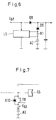
- FIG. 6 shows an example of a coupling circuit for the accumulator AI according to FIG. 1, which has a series diode D8 and a series circuit in the branch from a diode D9 and a resistor R1, with which the accumulator AI is in series.
- LS is a charging circuit that controls the coupling.
- the function of the diode D8 can optionally be taken over by one of the other components already present there. Due to the voltage drop across the resistor R1, the charge and discharge current of the accumulator AI can be controlled or monitored.
- the second switch SCH2 according to FIG. 1 is a transverse transistor T8, which is bridged by a diode D10, which is preferably its substrate diode.
- a MOSFET is suitable as transistor T8.
Landscapes
- Engineering & Computer Science (AREA)
- Power Engineering (AREA)
- Business, Economics & Management (AREA)
- Emergency Management (AREA)
- Computer Networks & Wireless Communication (AREA)
- Signal Processing (AREA)
- Charge And Discharge Circuits For Batteries Or The Like (AREA)
- Dc-Dc Converters (AREA)
- Direct Current Feeding And Distribution (AREA)
Applications Claiming Priority (2)
| Application Number | Priority Date | Filing Date | Title |
|---|---|---|---|
| DE4218852 | 1992-06-09 | ||
| DE4218852A DE4218852A1 (de) | 1992-06-09 | 1992-06-09 | Stromversorgungsschaltung für ein Funkgerät |
Publications (2)
| Publication Number | Publication Date |
|---|---|
| EP0573785A1 true EP0573785A1 (fr) | 1993-12-15 |
| EP0573785B1 EP0573785B1 (fr) | 1997-08-06 |
Family
ID=6460636
Family Applications (1)
| Application Number | Title | Priority Date | Filing Date |
|---|---|---|---|
| EP93107399A Expired - Lifetime EP0573785B1 (fr) | 1992-06-09 | 1993-05-07 | Circuit d'alimentation en courant électrique pour un appareil radio |
Country Status (3)
| Country | Link |
|---|---|
| US (1) | US5402056A (fr) |
| EP (1) | EP0573785B1 (fr) |
| DE (2) | DE4218852A1 (fr) |
Cited By (3)
| Publication number | Priority date | Publication date | Assignee | Title |
|---|---|---|---|---|
| EP0789947B1 (fr) * | 1994-10-31 | 2000-08-30 | Motorola, Inc. | Interrupteur de securite pour dispositif alimente par batterie |
| EP1145913A3 (fr) * | 2000-04-13 | 2004-12-01 | Volkswagen AG | Réseau de bord d'une automobile avèc stabilisateur de tension |
| CN110100363A (zh) * | 2017-03-17 | 2019-08-06 | 株式会社京滨 | 电路保护装置以及电压检测装置 |
Families Citing this family (11)
| Publication number | Priority date | Publication date | Assignee | Title |
|---|---|---|---|---|
| DE4340991A1 (de) * | 1993-12-01 | 1995-06-08 | Bosch Gmbh Robert | Spannungswandler |
| JP3661725B2 (ja) * | 1996-12-20 | 2005-06-22 | 旭硝子株式会社 | 電源装置 |
| US6097973A (en) * | 1997-12-19 | 2000-08-01 | Motorola, Inc. | Electronic circuit for a portable electronic device |
| DE19757362A1 (de) * | 1997-12-22 | 1999-06-24 | Nokia Mobile Phones Ltd | Spannungsversorgungsvorrichtung, insbesondere für ein Funktelefon in einem Kraftfahrzeug |
| DE19961435A1 (de) * | 1999-12-20 | 2001-06-21 | Volkswagen Ag | Verfahren und Vorrichtung zum Überspannungsschutz in Zweispannungsbordnetzen |
| FR2833113B1 (fr) * | 2001-11-30 | 2004-07-09 | Valeo Equip Electr Moteur | Convertisseur de courant electrique continu en courant continu reversible pour reseau bitension et reseau bitension equipe d'un tel convertisseur |
| US20040012368A1 (en) * | 2002-07-17 | 2004-01-22 | Massey Paul G. | Method and apparatus for charging a rechargeable cell |
| EP1532726B1 (fr) * | 2003-08-27 | 2006-10-11 | Fraunhofer-Gesellschaft zur Förderung der angewandten Forschung e.V. | Regulateur a decoupage |
| CN104167768B (zh) * | 2013-05-16 | 2018-05-15 | 中兴通讯股份有限公司 | 一种充电装置及充电方法 |
| WO2021156522A1 (fr) * | 2020-02-06 | 2021-08-12 | Diseño Y Construccion De Maquinaria Automatizada, S.L. | Station automatisée pour le salage de morceaux de viande et procédé de fonctionnement de celle-ci |
| CN114268146B (zh) * | 2021-12-07 | 2024-02-13 | 成都长城开发科技股份有限公司 | 低温环境下电子仪表的供电装置、方法 |
Citations (5)
| Publication number | Priority date | Publication date | Assignee | Title |
|---|---|---|---|---|
| GB2143094A (en) * | 1983-06-01 | 1985-01-30 | Epson Corp | Circuit for charging a secondary cell |
| DE3410719A1 (de) * | 1984-03-23 | 1985-10-03 | Ruhrkohle Ag, 4300 Essen | Tragbares stromversorgungsgeraet fuer grubenbaue |
| US4893348A (en) * | 1987-09-09 | 1990-01-09 | Mitsubishi Denki Kabushiki Kaisha | Power source control device in car telephone mobile station system |
| DE3923919A1 (de) * | 1988-07-19 | 1990-01-25 | Asahi Optical Co Ltd | Elektrische versorgungsquelle zum laden einer sekundaerversorgungsquelle |
| GB2249677A (en) * | 1990-10-19 | 1992-05-13 | Mitsubishi Electric Corp | Battery charger for mobile apparatus |
Family Cites Families (10)
| Publication number | Priority date | Publication date | Assignee | Title |
|---|---|---|---|---|
| US3821626A (en) * | 1973-06-18 | 1974-06-28 | United Aircraft Corp | Battery peaking unit for fuel cell power plants |
| US4056764A (en) * | 1974-06-03 | 1977-11-01 | Nissan Motor Company, Limited | Power supply system having two different types of batteries and current-limiting circuit for lower output battery |
| JPS5344386B2 (fr) * | 1974-06-10 | 1978-11-28 | ||
| US3900784A (en) * | 1974-07-10 | 1975-08-19 | Eltra Corp | Converter for battery charger |
| US4207511A (en) * | 1978-09-15 | 1980-06-10 | Ford Motor Company | Circuit for constant voltage power source |
| US4612492A (en) * | 1984-12-24 | 1986-09-16 | Burk Leslie L | Constant voltage power circuit for a remotely controlled device |
| JPS6217958A (ja) * | 1985-07-16 | 1987-01-26 | Sanyo Electric Co Ltd | 燃料電池発電システムの制御装置 |
| US4667142A (en) * | 1985-09-09 | 1987-05-19 | Tie/Communications, Inc. | Three-way power source circuit |
| JPH0217834A (ja) * | 1988-07-01 | 1990-01-22 | Matsushita Electric Works Ltd | 補助電池付電気機器 |
| US5218284A (en) * | 1990-12-31 | 1993-06-08 | Motorola, Inc. | Integral battery charging and supply regulation circuit |
-
1992
- 1992-06-09 DE DE4218852A patent/DE4218852A1/de not_active Withdrawn
-
1993
- 1993-05-07 US US08/058,093 patent/US5402056A/en not_active Expired - Fee Related
- 1993-05-07 DE DE59307051T patent/DE59307051D1/de not_active Expired - Fee Related
- 1993-05-07 EP EP93107399A patent/EP0573785B1/fr not_active Expired - Lifetime
Patent Citations (5)
| Publication number | Priority date | Publication date | Assignee | Title |
|---|---|---|---|---|
| GB2143094A (en) * | 1983-06-01 | 1985-01-30 | Epson Corp | Circuit for charging a secondary cell |
| DE3410719A1 (de) * | 1984-03-23 | 1985-10-03 | Ruhrkohle Ag, 4300 Essen | Tragbares stromversorgungsgeraet fuer grubenbaue |
| US4893348A (en) * | 1987-09-09 | 1990-01-09 | Mitsubishi Denki Kabushiki Kaisha | Power source control device in car telephone mobile station system |
| DE3923919A1 (de) * | 1988-07-19 | 1990-01-25 | Asahi Optical Co Ltd | Elektrische versorgungsquelle zum laden einer sekundaerversorgungsquelle |
| GB2249677A (en) * | 1990-10-19 | 1992-05-13 | Mitsubishi Electric Corp | Battery charger for mobile apparatus |
Cited By (5)
| Publication number | Priority date | Publication date | Assignee | Title |
|---|---|---|---|---|
| EP0789947B1 (fr) * | 1994-10-31 | 2000-08-30 | Motorola, Inc. | Interrupteur de securite pour dispositif alimente par batterie |
| EP1145913A3 (fr) * | 2000-04-13 | 2004-12-01 | Volkswagen AG | Réseau de bord d'une automobile avèc stabilisateur de tension |
| CN110100363A (zh) * | 2017-03-17 | 2019-08-06 | 株式会社京滨 | 电路保护装置以及电压检测装置 |
| CN110100363B (zh) * | 2017-03-17 | 2021-07-27 | 株式会社京滨 | 电路保护装置以及电压检测装置 |
| US11223193B2 (en) | 2017-03-17 | 2022-01-11 | Hitachi Astemo, Ltd. | Circuit protection device and voltage detection device |
Also Published As
| Publication number | Publication date |
|---|---|
| DE4218852A1 (de) | 1993-12-16 |
| EP0573785B1 (fr) | 1997-08-06 |
| US5402056A (en) | 1995-03-28 |
| DE59307051D1 (de) | 1997-09-11 |
Similar Documents
| Publication | Publication Date | Title |
|---|---|---|
| EP0573785B1 (fr) | Circuit d'alimentation en courant électrique pour un appareil radio | |
| DE2937995A1 (de) | Brueckenmischschaltung und verfahren zu deren betrieb | |
| DE102018126780A1 (de) | Schaltungsanordnung von Gate-Treiber-Schaltungen und Leistungsschaltern mit negativer Sperrspannung | |
| DE102014107815A1 (de) | System und Verfahren zum Ansteuern von Transistoren | |
| EP0326220B1 (fr) | Disposition de circuit pour alimenter une charge | |
| EP0982862B1 (fr) | Circuit bipolaire en pont sans résistances | |
| DE10144591C2 (de) | Schaltungsanordnung zur Spannungsregelung | |
| DE2223376A1 (de) | Schutzschaltung fuer einen schalttransistor im induktiven lastkreis | |
| DE3741221C1 (de) | Anordnung zum Befreien eines Halbleiterschalters vor hoher Sperrspannungsbeanspruchung sowie Anwendung hierzu | |
| EP0057910B1 (fr) | Circuit pour l'alimentation régulée d'un utilisateur | |
| EP1249066B1 (fr) | Appareil électrique comportant un motoeur électrique et un convertisseur à inductance | |
| DE3221404A1 (de) | Stromversorgungsschaltung | |
| DE10041475C2 (de) | Schaltnetzteil | |
| WO2004045250A1 (fr) | Circuit permettant de faire fonctionner au moins une diode electroluminescente | |
| DE102004012310A1 (de) | Tief-Hochsetzsteller | |
| DE102011117387B4 (de) | Spannungsversorgung | |
| EP0811529B1 (fr) | Dispositif de commutation avec faible tolérance de rayonnement électro-magnétique | |
| DE10257908A1 (de) | Getaktete Leistungsversorgung | |
| EP0798840B1 (fr) | Dispositif de batterie comme source d'alimentation | |
| EP0806827B1 (fr) | Circuit de protection contre l'inversion des bornes de la batterie | |
| DE4105942C2 (de) | Anlaufschaltung fuer eine steuerschaltung | |
| EP0234413B1 (fr) | Disposition de circuit pour alimentation de courant | |
| DE102014106578A1 (de) | Schaltung mit leistungsfaktorkorrekturfilter und gleichrichter oder inverter | |
| WO2025093206A1 (fr) | Dispositif de commutation pour un module électronique de puissance avec fonction d'amortissement pour transitoires de tension provoqués par une vitesse de mise en circuit | |
| DE102022103824A1 (de) | Bereitstellen von zwei voneinander unterschiedlichen elektrischen Gleichspannungen mittels eines Energiewandlers |
Legal Events
| Date | Code | Title | Description |
|---|---|---|---|
| PUAI | Public reference made under article 153(3) epc to a published international application that has entered the european phase |
Free format text: ORIGINAL CODE: 0009012 |
|
| AK | Designated contracting states |
Kind code of ref document: A1 Designated state(s): DE FR GB IT SE |
|
| 17P | Request for examination filed |
Effective date: 19940513 |
|
| 17Q | First examination report despatched |
Effective date: 19951124 |
|
| GRAG | Despatch of communication of intention to grant |
Free format text: ORIGINAL CODE: EPIDOS AGRA |
|
| GRAH | Despatch of communication of intention to grant a patent |
Free format text: ORIGINAL CODE: EPIDOS IGRA |
|
| GRAH | Despatch of communication of intention to grant a patent |
Free format text: ORIGINAL CODE: EPIDOS IGRA |
|
| GRAA | (expected) grant |
Free format text: ORIGINAL CODE: 0009210 |
|
| AK | Designated contracting states |
Kind code of ref document: B1 Designated state(s): DE FR GB IT SE |
|
| ET | Fr: translation filed | ||
| REF | Corresponds to: |
Ref document number: 59307051 Country of ref document: DE Date of ref document: 19970911 |
|
| ITF | It: translation for a ep patent filed | ||
| GBT | Gb: translation of ep patent filed (gb section 77(6)(a)/1977) |
Effective date: 19971023 |
|
| PGFP | Annual fee paid to national office [announced via postgrant information from national office to epo] |
Ref country code: GB Payment date: 19980428 Year of fee payment: 6 |
|
| RAP2 | Party data changed (patent owner data changed or rights of a patent transferred) |
Owner name: MOTOROLA, INC. |
|
| PGFP | Annual fee paid to national office [announced via postgrant information from national office to epo] |
Ref country code: SE Payment date: 19980527 Year of fee payment: 6 Ref country code: FR Payment date: 19980527 Year of fee payment: 6 |
|
| PLBE | No opposition filed within time limit |
Free format text: ORIGINAL CODE: 0009261 |
|
| PGFP | Annual fee paid to national office [announced via postgrant information from national office to epo] |
Ref country code: DE Payment date: 19980722 Year of fee payment: 6 |
|
| 26N | No opposition filed | ||
| PG25 | Lapsed in a contracting state [announced via postgrant information from national office to epo] |
Ref country code: GB Free format text: LAPSE BECAUSE OF NON-PAYMENT OF DUE FEES Effective date: 19990507 |
|
| PG25 | Lapsed in a contracting state [announced via postgrant information from national office to epo] |
Ref country code: SE Free format text: LAPSE BECAUSE OF NON-PAYMENT OF DUE FEES Effective date: 19990508 |
|
| GBPC | Gb: european patent ceased through non-payment of renewal fee |
Effective date: 19990507 |
|
| EUG | Se: european patent has lapsed |
Ref document number: 93107399.3 |
|
| PG25 | Lapsed in a contracting state [announced via postgrant information from national office to epo] |
Ref country code: FR Free format text: LAPSE BECAUSE OF NON-PAYMENT OF DUE FEES Effective date: 20000131 |
|
| PG25 | Lapsed in a contracting state [announced via postgrant information from national office to epo] |
Ref country code: DE Free format text: LAPSE BECAUSE OF NON-PAYMENT OF DUE FEES Effective date: 20000301 |
|
| REG | Reference to a national code |
Ref country code: FR Ref legal event code: ST |
|
| PG25 | Lapsed in a contracting state [announced via postgrant information from national office to epo] |
Ref country code: IT Free format text: LAPSE BECAUSE OF NON-PAYMENT OF DUE FEES;WARNING: LAPSES OF ITALIAN PATENTS WITH EFFECTIVE DATE BEFORE 2007 MAY HAVE OCCURRED AT ANY TIME BEFORE 2007. THE CORRECT EFFECTIVE DATE MAY BE DIFFERENT FROM THE ONE RECORDED. Effective date: 20050507 |