EP0573861A2 - SDH Funkkommunikationssystem und Sende-/Empfangseinrichtung hierzu - Google Patents
SDH Funkkommunikationssystem und Sende-/Empfangseinrichtung hierzu Download PDFInfo
- Publication number
- EP0573861A2 EP0573861A2 EP93108675A EP93108675A EP0573861A2 EP 0573861 A2 EP0573861 A2 EP 0573861A2 EP 93108675 A EP93108675 A EP 93108675A EP 93108675 A EP93108675 A EP 93108675A EP 0573861 A2 EP0573861 A2 EP 0573861A2
- Authority
- EP
- European Patent Office
- Prior art keywords
- frame
- radio
- stm
- radio communication
- timing
- Prior art date
- Legal status (The legal status is an assumption and is not a legal conclusion. Google has not performed a legal analysis and makes no representation as to the accuracy of the status listed.)
- Granted
Links
Images



Classifications
-
- H—ELECTRICITY
- H04—ELECTRIC COMMUNICATION TECHNIQUE
- H04J—MULTIPLEX COMMUNICATION
- H04J3/00—Time-division multiplex systems
- H04J3/16—Time-division multiplex systems in which the time allocation to individual channels within a transmission cycle is variable, e.g. to accommodate varying complexity of signals, to vary number of channels transmitted
- H04J3/1605—Fixed allocated frame structures
- H04J3/1611—Synchronous digital hierarchy [SDH] or SONET
-
- H—ELECTRICITY
- H04—ELECTRIC COMMUNICATION TECHNIQUE
- H04J—MULTIPLEX COMMUNICATION
- H04J2203/00—Aspects of optical multiplex systems other than those covered by H04J14/05 and H04J14/07
- H04J2203/0001—Provisions for broadband connections in integrated services digital network using frames of the Optical Transport Network [OTN] or using synchronous transfer mode [STM], e.g. SONET, SDH
- H04J2203/0028—Local loop
- H04J2203/003—Medium of transmission, e.g. fibre, cable, radio
- H04J2203/0035—Radio
Definitions
- the present invention relates to an SDH (Synchronous Digital Hierarchy) radio communication system and a transmitter/receiver equipment therefor.
- SDH Serial Digital Hierarchy
- CCITT International Telegraph and Telephone Consultative Committee
- STM Session Initiation Protocol
- CCITT recommends the use of three kinds of STMs: STM-1 (Synchronous Transport Module Level 1 with a bit rate of 155520 kb/s), STM-4 (Synchronous Transport Module level 4 with a bit rate of 622080 kb/s), and STM-16 (Synchronous Transport Module level 16 with a bit rate of 2488320 kb/s).
- TTC Transmission Control Committee
- STM-0 Session Telephone Committee
- STM-4 or STM-16 is expressed as STM-N
- a frame of STM-N is expressed as STM frame.
- the STM includes information called SOH (Section Overhead) in addition to data to be communicated.
- SOH Section Overhead
- the SOH is comprised of an STM frame synchronizing byte for synchronization between STM frames on the sides of transmission and reception, and of a OW (Order Wire) for delivery of information among nodes.
- prior art radio communication with use of SDH is adapted such that an STM frame is divided into subframes of a predetermined size, to each of which subframes there is added an RFCOH(Radio Frame Complementary Overhead) composed of a radio frame synchronizing bits for synchronization of a radio frame on the sides of transmission and reception and an error control bits for correcting transmission error, and each of which subframes serves as a radio frame for communication.
- RFCOH Radio Frame Complementary Overhead
- the prior art communication system includes as described above synchronizing bytes (STM frame synchronizing byte and radio frame synchronizing byte) each for synchronization of the STM frame and of the radio frame, those bytes having no relation to the sizes of the STM frame and the radio frame.
- STM frame synchronizing byte and radio frame synchronizing byte each for synchronization of the STM frame and of the radio frame, those bytes having no relation to the sizes of the STM frame and the radio frame.
- FIG.1 there is illusrated a block diagram of a transmitter/receiver apparatus for use in a prior art SDH radio communication system.
- a transmitting station serves as follows.
- An STM frame synchronization circuit 2A detects STM frame synchronizing byte in an SOH of an STM frame 101A as inputted and issues an STM frame pulse 102A at a timing when the afore-mentioned STM frame synchronizing byte is detected.
- An STM signal processing circuit 1A extracts the SOH from the STM frame 101A at a timing of the STM frame pulse 102A, and again inserts the SOH into the STM frame 101 A after the SOH is subject to a required processing by another circuit not illustrated and issues it as an STM frame 101 B.
- a radio frame pulse generating circuit 4A frequency-divides a rate converting clock 104A supplied from a rate converting circuit 3A, and issues a radio frame pulse 106A.
- the rate converting circuit 3A forms in the STM frame 101 B empty time slots for the RFCOH on the basis of the radio frame pulse 106A together with rate conversion of the same STM frame 101 B, and inserts a predetermined RFCOH into the empty time slots so formed and issues it as a radio frame 107.
- a receiving station serves as follows.
- a radio frame synchronization circuit 5B detects the radio frame synchronizing bits in the RFCOH of the received radio frame 107, and issues a radio frame pulse 106B at a timing when the radio frame synchronizing bits is detected.
- a rate converting circuit 3B extracts the RFCOH from the radio frame 107 at a timing of the radio frame pulse 106B, together with the elimination of the time slot for the RFCOH and the rate conversion of the same to issue it as an STM frame 101 C.
- An STM frame synchronous circuit 2B detects the STM frame synchronizing byte in the SOH of the STM frame 101C, and issues an STM frame pulse 102B at a timing when the STM frame synchronizing byte is detected.
- a STM signal processing circuit 1B extracts the SOH from the STM frame 101 C at the timing of the STM frame pulse 102B, and again inserts the SOH into the STM frame 101 C after processing as required the SOH with use of another circuit (not shown) and issues the same as an STM frame 101D.
- the present invention In view of the drawbacks with the prior art, it is an object of the present invention to simplify the circuit construction of a transmitter/receiver equipment to reduce power consumption.
- the present invention In the case where an intermediate radio station is installed, the present invention has another object to simplify the circuit construction of the intermediate station to reduce power consumption.
- An SHD radio commuincation system of the present invention is adapted in another aspect such that said overhead bits for radio communication includes no radio communication frame synchronizing bits.
- An SDH radio communication transmitter equipment is adapted in one aspect such that it comprises an STM frame synchronization circuit wherein frames of synchronous transport modules in synchronous digital hierarchy are inputted, and an STM frame synchronizing byte in a section overhead of a frame of said synchronous transport module is detected, and further an STM frame pulse is issued at a timing when said STM frame synchronizing byte is detected, an STM signal processing circuit for extracting the section overhead from the frame of said synchronous transport module based upon the timing of said STM frame pulse and inserting the section overead into the frame of said synchronous transport module, a radio frame multiplying circuit for multiplying the frequency of said STM frame pulse by K (a natural number other than 0) and issuing a radio frame pulse at a timing K times the timing of the STM frame pulse, and a rate converting circuit for inserting the radio communication overhead bits into the frame of said synchronous transport module to alter it to a radio frame and performing rate conversion of the just-mentioned radio frame.
- K a natural number other
- An SDH radio communication receiver equipment is adapted in one aspect such that it comprises an STM frame synchronization circuit for receiving radio frames of SDH radio communication, and detecting an STM frame synchronizing byte in a section overhead of each frame of a synchronous transport module in synchronous digital hierarchy in said radio frame, a radio frame multiplying circuit or multiplying the frequency of said STM frame pulse by (a natural number other than 0) to issue a radio frame pulse at a timing K times the timing of said STM frame pulse, a rate converting circuit for extracting the radio commuincation secion overhead having no radio comunication frame synchronizing bits from said radio frame based upon the timing of said radio frame pulse as a frame of the synchronous transport module and performing rate conversion of the frame of said synchronous transport module, and an STM signal processing circuit for extracting the section overhead from said synchronous tarn- sport module based upon the timing of said STM frame pulse and inserting the section overhead of said synchronous transport module.
- An SDH radio cmmunication receiver equipment of the present invention is adapted in another aspect such that it further comprises the SDH radio communication transmitter equipment as recited in the foregoing and the SDH radio communication receiver equipment recited in the foregoing.
- the SDH radio communication transmitter equipment of the present invention recited in the foregoing is adapted in another aspect such that the radio comunication overhead bits which is inserted into the frame of the synchronous transport module in said rate converting circuit has no radio communication frame synchronizing bits.
- the SDH radio receiver equipment of the present invention recited in the foregoing is adapted in another aspect such that the radio frame inputted in said STM frame synchronization circuit has no radio communication frame synchronizing bits in the radio communication overhead bits of said radio frame.
- An SDH radio communication transmitter/receiver equipment of the present invention comprises the SDH radio communication transmitter apparatus recited in the foregoing and the SDH radio communication receiver equipment recited in the foregoing.
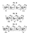
- FIGs.2A to 2C there are illustrated in block diagrams a transmitting terminal station, an intermediate station, and a receiving terminal station in a first embodiment with use of an SDH radio communication system according to the present invention.
- the transmitting terminal station will first be described.
- an STM frame terminating circuit 301 detects a STM frame synchronizing byte in SOH of an STM frame 31 as inputted, and extracts the SOH from the STM frame 31 in the timing of the detection, and further again inserts the SOH into the STM fram 31 after processing the SOH as required with another circuit not illustrated and outputs it as an STM frame 32.
- a row converting circuit 302 converts the STM frame 32 to an "n" row signal of a 2" modulation system for radio communication system, and outputs a converted "n” row STM signal 33.
- a radio frame multiplexing circuit 304 inserts RFCOH into the empty time slot in the rate converted STM signal 34 based upon the radio frame pulse 35, and issues a radio frame 36.
- a radio frame demultiplexing circuit 305 detects a radio frame synchronizing bits in RFCOH of a radio frame 41 received from the transmitting terminal station or another intermeiate station, and issues an STM signal 42 in the timing of the detection after separating the RFCOH from the radio frame 41, and further issues a radio frame pulse 43 in the timing of the detection of the radio frame synchronizing bits in the RFCOH.
- the STM signal 42 includes the time slot for RFCOH left behind intactly.
- the SOH terminating circuit 306 further issues a STM signal 44 which is a signal where OW information is updated with respect to the SOH in the STM signal 42, and issues a radio frame pulse 45 in the timing of the time slot for RFCOH of the STM signal 44.
- STM signal 44 is a signal where OW information is updated with respect to the SOH in the STM signal 42, and issues a radio frame pulse 45 in the timing of the time slot for RFCOH of the STM signal 44.
- a radio frame multiplexing circuit 307 inserts RFCOH into the time slot for the RFCOH of the STM signal 44 based upon the radio frame 46.
- a radio frame demultiplexing circuit 308 detects a radio frame synchronizing bits in RFCOH of a radio frame 51 received from the transmiting terminal station and outputs an STM signal 52 in the timing of the detection after separating the RFCOH from the radio frame 51 and further issues a radio frame pulse 53 in the timing of the detection of the radio frame synchronizing bits in the RFCOH. It is noticed herein that the STM signal 52 includes the time slot for the RFCOH left behind intactly.
- a rate converting circuit 309 eliminates the time slot for the RFCOH from the STM signal 52 and smooths the same on the basis of the radio frame pulse 53, and outputs an STM signal 54 (i.e., "n" row) after the rate conversion.
- a row converting circuit 310 converts the "n" row STM signal 54 to a one row STM frame 55.
- An STM frame terminating circuit 311 detects a STM frame synchronizing byte in SOH of the STM frame 55, and extracts the SOH from the STM frame 55 in the timing of the detection, and again inserts the SOH into the STM frame 55 after processing the SOH as required with another circuit not illustrated and issues the same to a later stage circuit as a STM frame 56.
- FIG.3 there is illustrated in a block diagram a transmitter/receiver equipment for use in the SDH radio communication system of the present invention.
- FIG.4 there is illustrated a signal format in the transmitter/receiver equipment illustrated in FIG.3.
- an STM frame synchronization circuit 12A detects an STM frame synchronzing byte in SOH of an STM frame 111A as inputted, and issues an STM frame pulse 112A in the timing of the detection.
- the format of the STM frame 111 and the timing of the STM frame pulse 112A are as illustrated in FIG.4, and in the present embodiment the bit number of one STM frame is assumed to be S bits.
- An STM signal processing circuit 11 A extracts the SOH from the STM frame 111A in the timing of the STM frame pulse 112A, and again inserts the SOH into the STM frame 111A after processing the SOH as required with another cicuit not illustrated and outputs the same as an STM frame 111 B.
- the format of the STM frame 111 B is illustrated in FIG.4.
- a radio frame multiplying circuit 16A issues a radio frame pulse 13A of a frequency K times (K is a natural number other than 0) that of the STM frame pulse 112A.
- the timing of the radio frame pulse 113A is as illustratedin FIG.4 which illustrates a case where K is 2.
- a rate converting circuit 13A performs preparation of an empty time slot for RFCOH and rate conversion with respect to the STM frame 111 B on the basis of the radio frame pulse 113A, and inserts predetermined RFCOH into the empty time slot and outputs the same as a radio frame 115.
- the inserted RFCOH is set to include no radio frame synchronizing bits.
- the format of the radio frame 115 is illustrated in FIG.4.
- the rate conversion is done such that the bit rate of the radio frame 115 is faster than that of the STM frame 111 B by a fraction of the added RFCOH.
- a STM frame synchronization circuit 12B detects an STM frame synchronizing byte in SOH of the received radio frame 115, and issues an STM frame pulse 112B in the timing of the detection.
- the timing of the STM frame pulse 112B is as illustrated in FIG.4.
- a radio frame multiplying circuit 16B issues a radio frame pulse 113B of a frequency K times (K is a natural number other than 0) that of the STM frame pulse 112B.
- K is a natural number other than 0
- the timing of the radio frame pulse 113B is as illustrated in FIG.4 where K is 2.
- a rate converting circuit 3B matches the phase of the radio frame pulse 113B with that of a clock of the radio frame 115 and thereafter extracts the RFCOH from the radio frame 115 in the timing of the radio frame pulse 113B, and performs elimination of the timing slot for the RFCOH and rate conversion and thereafter outputs it as an STM frame 111 C.
- An STM signal processing circuit 11 B extracts the SOH from the STM frame 111 C in the timing of the STM frame pulse 112B, and again inserts the SOH into the STM frame 111 C after editing the SOH with another circuit not illustrated and outputs it to a later stage circuit as an STM frame 111 D.
- FIG.5 the details of the transmitting station is illustrated in the block diagram of the transmitter/receiver apparatus for use in the SDH radio communication system of the present invention illustrated in FIG.3.
- An STM frame synchronization circuit 12A of FIG.3 is comprised of an STM frame pulse generating circuit 202 and an STM frame detecting circuit 201.
- An STM frame pulse generating circuit 202 frequency-divides an input clock WCLK to prepare an STM frame pulse SFP of the same frequency as a frame width of the STM frame, and prepares an STM frame synchronizing byte pattern FPN in synchronism with the STM frame pulse SFP.
- An STM frame detecting circuit 201 detects the STM frame synchronizing byte in the SOH of the STM frame 111A by comparing the STM frame 111A as inputted with the STM frame synchronizing byte pattern FPN.
- the STM frame detecting circuit 201 feeds a control signal CP1 to the STM frame pulse generatng circuit 202 continuouslly till the detection of the STM frame synchronizing byte.
- the STM frame pulse generating circuit 202 shifts the STM frame pulse SFP in its phase once receiving the control signal CP1, and issues hereby an STM frame pulse SFP in synchronism with the STM frame synchronizing byte in the SOH of the STM frame 111 A.
- the STM signal processing circuit 11 A of FIG.2 is comprised of an SOH processing circuit 203 and an STM frame timing generating circuit 204.
- the STM frame timing generating circuit 202 shifts the STM frame pulse SP from the STM frame pulse generating circuit 202 in its phase, and issues an SOH timing pulse STP in synchronism with the head of the SOH of the STM frame 111 A.
- the SOH processing circuit 203 extracts the SOH from the STM frame 111 A on the basis of the foregoing SOH timing pulse STP, and again inserts the SOH into the STM frame 111 A after editing the SOH in another circuit not illustrated and outputs it as a STM frame D2.
- the rate converting circuit 13A of FIG.3 is comprised of an elastic memory 208, a write pulse generating circuit 205, a read pulse generating circuit 206, a PLL circuit 207, and a RFCOH inserting circuit 211.
- a write pulse generating circuit 205 frequency-divides an input clock WCLK based upon the STM frame pulse SFP to issue a write pulse WP.
- the read pulse generating circuit 206 interrupts delivery of the result of frequency division of a clock RCLK after rate conversion of the same with use of a RFCOH timing pulse RTP prepared in a radio frame timing generating circuit 209, and issues a read pulse RP of the same frequency as that of the write pulse WP.
- the PLL circuit 207 issues the clock RCLK after the rate converion using the write pulse WP and the read pulse RP as an input for phase comparison.
- the elastic memory 208 executes rate conversion of the empty time slot for the RFCOH by writing in a memory the STM frame D2 from the SOH processing circuit 203 in the timing of the write pulse WP and reading the same from the memory in the timing of the read pulse RP, and outputs a radio frame D3 where an empty time slot for RFCOH prepared and rate-converted.
- the RFCOH inserting circuit 211 inserts RFCOH into the empty time slot for the RFCOH of the radio frame D3 on the basis of the RFCOH timing pulse RTP, and issues it as a radio frame 115.
- the radio frame multiplying circuit 16A of FIG.3 is comprised of a radio frame timing generating circuit 209 and a radio frame timing detecting circuit 210.
- the radio frame timing generating circuit 209 frequency-divides the clock RCLK after rate conversion, and issues a RFCOH timing pulse RTP of the same period as that of the radio frame and ouputs it to the radio frame timing detecting circuit 210.
- the radio frame timing detecting circuit 210 prepares a reference pulse of the same phase as that of the STM frame pulse SFP but of the frequency K times as that of the same (K is a natural number other than 0), and compares the RFCOH timing pulse RTP with the reference pulse and feeds a control signal CP2 to the radio frame timing generating circuit 209 until coincidence of the comparison is attained.
- the radio frame timing generating circuit 209 shifts the RFCOH timing pulse RTP in its phase once receiving the control signal CP2 and hereby issues the RFCOH timing pulse RTP in synchronism with the location of the RFCOH empty time slot of the radio frame D3.
- M is a natural number other than 0. Accordingly, in the case where the SOH of the STM frame is terminated in the intermediate station, the need of a rate converting circuit is eliminated together with the simplification of the circuit constrcution of the intermediate station and together with the reduction of consumed power.
- synchronization is established for the radio frame and for the STM frame using the STM frame synchronizing byte in the SOH of the STM frame. Accordingly, only one frame synchronization circuit is simply required and the radio frame pulse is generated only with a simplified multiplying circuit. Thus, the circuit construction of the transmitter/receiver equipment is simplified and power consumption is reduced. Moreover, the frame synchronization is simply required only once, and hence frame alignment for synchronization time is reduced. Additionally, there is no need of providing a radio frame synchronizing bits in the RFCOH (an overhead of a radio frame), so that temporal bandwidth of radio communication is narrowed and interference between adjacent waves is reduced.
- RFCOH an overhead of a radio frame
Landscapes
- Engineering & Computer Science (AREA)
- Computer Networks & Wireless Communication (AREA)
- Signal Processing (AREA)
- Synchronisation In Digital Transmission Systems (AREA)
- Time-Division Multiplex Systems (AREA)
Applications Claiming Priority (3)
| Application Number | Priority Date | Filing Date | Title |
|---|---|---|---|
| JP13740992 | 1992-05-29 | ||
| JP13740992 | 1992-05-29 | ||
| JP137409/92 | 1992-05-29 |
Publications (3)
| Publication Number | Publication Date |
|---|---|
| EP0573861A2 true EP0573861A2 (de) | 1993-12-15 |
| EP0573861A3 EP0573861A3 (de) | 1994-02-02 |
| EP0573861B1 EP0573861B1 (de) | 2000-08-30 |
Family
ID=15197972
Family Applications (1)
| Application Number | Title | Priority Date | Filing Date |
|---|---|---|---|
| EP93108675A Expired - Lifetime EP0573861B1 (de) | 1992-05-29 | 1993-05-28 | SDH Funkkommunikationssystem und Sende-/Empfangseinrichtung hierzu |
Country Status (4)
| Country | Link |
|---|---|
| US (1) | US5481547A (de) |
| EP (1) | EP0573861B1 (de) |
| AU (1) | AU663590B2 (de) |
| DE (1) | DE69329310T2 (de) |
Cited By (3)
| Publication number | Priority date | Publication date | Assignee | Title |
|---|---|---|---|---|
| US5898887A (en) * | 1995-11-24 | 1999-04-27 | Dsc Communications A/S | Receiver unit for a data transmission system |
| EP0921651A1 (de) * | 1997-12-08 | 1999-06-09 | Alcatel | Funkübertragungssystem mit konfigurierbarer Übertragungskapazität, entsprechende Sender und Empfänger |
| EP1150447A3 (de) * | 2000-03-17 | 2004-01-07 | Alcatel | Verfahren und Vorrichtung zum Senden und Empfangen von höherwertigen digitalen Signalen über zwei Funkfrequenzträgern in einer Funkregenerierungssektion |
Families Citing this family (8)
| Publication number | Priority date | Publication date | Assignee | Title |
|---|---|---|---|---|
| JP3446799B2 (ja) * | 1996-12-24 | 2003-09-16 | 富士通株式会社 | 加入者系伝送装置 |
| JPH1174878A (ja) * | 1997-08-28 | 1999-03-16 | Mitsubishi Electric Corp | デジタルデータ伝送システム |
| JP2001024565A (ja) * | 1999-07-08 | 2001-01-26 | Fujitsu Ltd | 複数回線の無瞬断切替え制御器を有する伝送システム |
| IT1314145B1 (it) * | 1999-12-21 | 2002-12-04 | Cit Alcatel | Metodo e dispositivo per convertire un segnale stm-1 in un segnale sub-stm-1 e vice-versa in trasmissioni radio |
| US6931006B1 (en) * | 2000-12-22 | 2005-08-16 | Applied Micro Circuits Corporation | System and method for selectively broadcasting a multidimensional digital frame structure |
| GB0100094D0 (en) * | 2001-01-03 | 2001-02-14 | Vtech Communications Ltd | System clock synchronisation using phased-lock loop |
| EP2923474A4 (de) * | 2012-11-26 | 2016-06-29 | Adc Telecommunications Inc | Zeitschlitz-mapping- und/oder aggregationselement für digitale funkfrequenztransportarchitektur |
| CN105122757B (zh) | 2012-11-26 | 2018-12-18 | Adc电信股份有限公司 | 灵活、可重新配置的多点至多点数字射频输送架构 |
Family Cites Families (8)
| Publication number | Priority date | Publication date | Assignee | Title |
|---|---|---|---|---|
| US4215245A (en) * | 1978-12-29 | 1980-07-29 | Bell Telephone Laboratories, Incorporated | Variable rate synchronous digital transmission system |
| FR2500240B1 (fr) * | 1981-02-19 | 1986-10-31 | Billy Jean Claude | Systeme de multiplexage et de demultiplexage avec justification |
| DE3238973A1 (de) * | 1982-10-21 | 1984-04-26 | Siemens AG, 1000 Berlin und 8000 München | Verfahren zur digitalen nachrichtenuebertragung |
| US4807221A (en) * | 1984-11-27 | 1989-02-21 | Siemens Aktiengesellschaft | Digital signal multiplex device |
| US5241543A (en) * | 1989-01-25 | 1993-08-31 | Hitachi, Ltd. | Independent clocking local area network and nodes used for the same |
| DE3934248A1 (de) * | 1989-10-13 | 1991-04-18 | Standard Elektrik Lorenz Ag | Multiplexer und demultiplexer, insbesondere fuer nachrichtenuebertragungs-netze mit einer synchronen hierarchie der digitalsignale |
| DE3942883A1 (de) * | 1989-12-23 | 1991-06-27 | Philips Patentverwaltung | Schaltungsanordnung zur bitratenanpassung |
| JP2600509B2 (ja) * | 1990-09-05 | 1997-04-16 | 富士通株式会社 | ディジタル無線伝送方式 |
-
1993
- 1993-05-28 US US08/068,970 patent/US5481547A/en not_active Expired - Lifetime
- 1993-05-28 DE DE69329310T patent/DE69329310T2/de not_active Expired - Lifetime
- 1993-05-28 EP EP93108675A patent/EP0573861B1/de not_active Expired - Lifetime
- 1993-05-28 AU AU39871/93A patent/AU663590B2/en not_active Ceased
Cited By (4)
| Publication number | Priority date | Publication date | Assignee | Title |
|---|---|---|---|---|
| US5898887A (en) * | 1995-11-24 | 1999-04-27 | Dsc Communications A/S | Receiver unit for a data transmission system |
| EP0921651A1 (de) * | 1997-12-08 | 1999-06-09 | Alcatel | Funkübertragungssystem mit konfigurierbarer Übertragungskapazität, entsprechende Sender und Empfänger |
| FR2772220A1 (fr) * | 1997-12-08 | 1999-06-11 | Alsthom Cge Alcatel | Systeme de transmission par voie hertzienne a capacite de transmission configurable, emetteur et recepteur correspondants |
| EP1150447A3 (de) * | 2000-03-17 | 2004-01-07 | Alcatel | Verfahren und Vorrichtung zum Senden und Empfangen von höherwertigen digitalen Signalen über zwei Funkfrequenzträgern in einer Funkregenerierungssektion |
Also Published As
| Publication number | Publication date |
|---|---|
| AU3987193A (en) | 1993-12-02 |
| EP0573861A3 (de) | 1994-02-02 |
| AU663590B2 (en) | 1995-10-12 |
| EP0573861B1 (de) | 2000-08-30 |
| US5481547A (en) | 1996-01-02 |
| DE69329310T2 (de) | 2001-01-18 |
| DE69329310D1 (de) | 2000-10-05 |
Similar Documents
| Publication | Publication Date | Title |
|---|---|---|
| US5241543A (en) | Independent clocking local area network and nodes used for the same | |
| US5065396A (en) | Inverse multiplexer and demultiplexer techniques | |
| US3995120A (en) | Digital time-division multiplexing system | |
| US5481547A (en) | SDH radio communication system and transmitter/receiver equipment therefor | |
| US7042908B1 (en) | Method and apparatus for transmitting arbitrary electrical signals over a data network | |
| KR100871218B1 (ko) | 이동통신 시스템에서 기지국의 주 장치와 원거리 장치간데이터 송/수신 장치 | |
| US5331630A (en) | Renewal method and apparatus for AU-4 and TU-3 pointers of synchronous digital hierarchy | |
| KR19990009018A (ko) | 비동기 전송 모드망과 플레스이오크로너스 디지탈 계층구조 망간의 접속에 따른 지터와 원더 감소 장치 | |
| US20020067746A1 (en) | Apparatus for transmitting multi-frame in multiplex transmission and method of doing the same | |
| JP2546970B2 (ja) | Sdh無線通信方式および送受信装置 | |
| JP3246423B2 (ja) | 網同期装置 | |
| JPH06141014A (ja) | Sdh伝送方式 | |
| KR100271311B1 (ko) | 광가입자 전송장치에서의 관리단위신호에 대한 관리단위 포인터및 계위단위 포인터 처리장치 | |
| KR100284007B1 (ko) | 광가입자 전송장치에 있어서 계위단위그룹 신호와 ds1 신호 사이의 역다중화 장치 | |
| KR930007133B1 (ko) | 동기식 다중장치의 대기시간지터 감소회로 | |
| KR950001507B1 (ko) | 가상 컨테이너 12신호 사상기 | |
| JPH05327642A (ja) | フレーム変換方法及び変換回路 | |
| JPH04263531A (ja) | ディジタル無線伝送方式 | |
| JP2976732B2 (ja) | 同期光多重化装置 | |
| JP2968599B2 (ja) | インタフェース回路 | |
| KR100922736B1 (ko) | 10GbE/STM-64 신호와0DU2/0TU2신호와의 정합 장치 및 그 정합 방법 | |
| JPH05244113A (ja) | データ伝送装置 | |
| JP2920650B2 (ja) | 情報伝送方法および装置 | |
| KR930004097B1 (ko) | 64Kbps 데이타 다중장치 | |
| JP3504554B2 (ja) | 時分割多重化データ通信システム並びにその送信機及び受信機 |
Legal Events
| Date | Code | Title | Description |
|---|---|---|---|
| PUAI | Public reference made under article 153(3) epc to a published international application that has entered the european phase |
Free format text: ORIGINAL CODE: 0009012 |
|
| PUAL | Search report despatched |
Free format text: ORIGINAL CODE: 0009013 |
|
| AK | Designated contracting states |
Kind code of ref document: A2 Designated state(s): DE NL SE |
|
| AK | Designated contracting states |
Kind code of ref document: A3 Designated state(s): DE NL SE |
|
| 17P | Request for examination filed |
Effective date: 19931228 |
|
| 17Q | First examination report despatched |
Effective date: 19970324 |
|
| GRAG | Despatch of communication of intention to grant |
Free format text: ORIGINAL CODE: EPIDOS AGRA |
|
| GRAG | Despatch of communication of intention to grant |
Free format text: ORIGINAL CODE: EPIDOS AGRA |
|
| GRAG | Despatch of communication of intention to grant |
Free format text: ORIGINAL CODE: EPIDOS AGRA |
|
| GRAH | Despatch of communication of intention to grant a patent |
Free format text: ORIGINAL CODE: EPIDOS IGRA |
|
| GRAH | Despatch of communication of intention to grant a patent |
Free format text: ORIGINAL CODE: EPIDOS IGRA |
|
| GRAA | (expected) grant |
Free format text: ORIGINAL CODE: 0009210 |
|
| AK | Designated contracting states |
Kind code of ref document: B1 Designated state(s): DE NL SE |
|
| REF | Corresponds to: |
Ref document number: 69329310 Country of ref document: DE Date of ref document: 20001005 |
|
| EN | Fr: translation not filed | ||
| PLBE | No opposition filed within time limit |
Free format text: ORIGINAL CODE: 0009261 |
|
| STAA | Information on the status of an ep patent application or granted ep patent |
Free format text: STATUS: NO OPPOSITION FILED WITHIN TIME LIMIT |
|
| 26N | No opposition filed | ||
| PGFP | Annual fee paid to national office [announced via postgrant information from national office to epo] |
Ref country code: NL Payment date: 20100518 Year of fee payment: 18 Ref country code: DE Payment date: 20100526 Year of fee payment: 18 |
|
| PGFP | Annual fee paid to national office [announced via postgrant information from national office to epo] |
Ref country code: SE Payment date: 20100510 Year of fee payment: 18 |
|
| REG | Reference to a national code |
Ref country code: DE Ref legal event code: R119 Ref document number: 69329310 Country of ref document: DE |
|
| REG | Reference to a national code |
Ref country code: DE Ref legal event code: R119 Ref document number: 69329310 Country of ref document: DE |
|
| REG | Reference to a national code |
Ref country code: NL Ref legal event code: V1 Effective date: 20111201 |
|
| REG | Reference to a national code |
Ref country code: SE Ref legal event code: EUG |
|
| PG25 | Lapsed in a contracting state [announced via postgrant information from national office to epo] |
Ref country code: NL Free format text: LAPSE BECAUSE OF NON-PAYMENT OF DUE FEES Effective date: 20111201 |
|
| PG25 | Lapsed in a contracting state [announced via postgrant information from national office to epo] |
Ref country code: DE Free format text: LAPSE BECAUSE OF NON-PAYMENT OF DUE FEES Effective date: 20111130 |
|
| PG25 | Lapsed in a contracting state [announced via postgrant information from national office to epo] |
Ref country code: SE Free format text: LAPSE BECAUSE OF NON-PAYMENT OF DUE FEES Effective date: 20110529 |