EP0574052B1 - Schaltungsanordnungen zur Farb-Hilfsträger-Frequenzregeneration und zur Farbartdemodulation - Google Patents
Schaltungsanordnungen zur Farb-Hilfsträger-Frequenzregeneration und zur Farbartdemodulation Download PDFInfo
- Publication number
- EP0574052B1 EP0574052B1 EP19930201328 EP93201328A EP0574052B1 EP 0574052 B1 EP0574052 B1 EP 0574052B1 EP 19930201328 EP19930201328 EP 19930201328 EP 93201328 A EP93201328 A EP 93201328A EP 0574052 B1 EP0574052 B1 EP 0574052B1
- Authority
- EP
- European Patent Office
- Prior art keywords
- signal
- burst
- frequency
- phase
- sin
- Prior art date
- Legal status (The legal status is an assumption and is not a legal conclusion. Google has not performed a legal analysis and makes no representation as to the accuracy of the status listed.)
- Expired - Lifetime
Links
Images


Classifications
-
- H—ELECTRICITY
- H04—ELECTRIC COMMUNICATION TECHNIQUE
- H04N—PICTORIAL COMMUNICATION, e.g. TELEVISION
- H04N9/00—Details of colour television systems
- H04N9/44—Colour synchronisation
- H04N9/45—Generation or recovery of colour sub-carriers
-
- H—ELECTRICITY
- H04—ELECTRIC COMMUNICATION TECHNIQUE
- H04N—PICTORIAL COMMUNICATION, e.g. TELEVISION
- H04N11/00—Colour television systems
- H04N11/06—Transmission systems characterised by the manner in which the individual colour picture signal components are combined
- H04N11/12—Transmission systems characterised by the manner in which the individual colour picture signal components are combined using simultaneous signals only
- H04N11/14—Transmission systems characterised by the manner in which the individual colour picture signal components are combined using simultaneous signals only in which one signal, modulated in phase and amplitude, conveys colour information and a second signal conveys brightness information, e.g. NTSC-system
- H04N11/16—Transmission systems characterised by the manner in which the individual colour picture signal components are combined using simultaneous signals only in which one signal, modulated in phase and amplitude, conveys colour information and a second signal conveys brightness information, e.g. NTSC-system the chrominance signal alternating in phase, e.g. PAL-system
-
- H—ELECTRICITY
- H04—ELECTRIC COMMUNICATION TECHNIQUE
- H04N—PICTORIAL COMMUNICATION, e.g. TELEVISION
- H04N9/00—Details of colour television systems
- H04N9/44—Colour synchronisation
- H04N9/465—Synchronisation of the PAL-switch
Definitions
- the invention relates to a color subcarrier frequency regeneration circuit comprising a burst phase detector for detecting the burst phase of a PAL signal.
- the invention also relates to a chrominance demodulation circuit in which the burst phase of a PAL signal is detected.
- the invention further relates to PAL video signal receivers.
- Such circuits for color subcarrier frequency regeneration and chrominance demodulation are disclosed in US-A-3,877,066.
- the color information is modulated on an alternating subcarrier. Therefore, a color subcarrier frequency reference signal burst is transmitted during each line of the television signal in the color burst period.
- the phase of this burst alternates from line to line between 135 degrees and 225 degrees.
- the burst phase is fixed and amounts to 180 degrees.
- this burst is used to regenerate an internal color frequency signal, which is phase-locked to the burst.
- a phase detector a reference signal from a voltage-controlled oscillator (VCO) is compared to the burst.
- VCO voltage-controlled oscillator
- a low-pass loop filter connects the phase detector output to a phase control input of the VCO.
- the combination of phase detector, low-pass loop filter and VCO constitutes a phase-locked loop.
- the desired control behavior is obtained by selecting a suitable loop gain and low-pass loop filter. To allow the loop to adjust rapidly to the color burst, the loop behavior should be fast, but in view of noise, the loop behavior should be slow; consequently, a compromise solution has to be found. Generally, a damping factor of 0,5 and a resonance frequency of 200 Hz are chosen.
- the optimum loop filter component values are generally determined by experiment. Moreover, in multistandard receivers, the same loop filter is used for both NTSC and PAL, so that the loop filter should be suitable for both standards. Further, when the burst phase is detected at an angle of ⁇ 45 degrees rather than 90 degrees, the signal-to-noise ratio at the phase detector output is 3 dB lower in the case of PAL signal reception as compared to NTSC signal reception.
- an object of the invention to provide a method of regenerating the color subcarrier frequency in which the detrimental effects of the alternating burst phase are mitigated.
- a color subcarrier frequency regeneration circuit as defined in claim 1.
- the invention provides chrominance demodulation circuits as defined in claims 2 and 3.
- the invention further provides PAL video signal receivers as defined in claims 4, 5 and 6.
- the invention is based on the recognition that when the reference signal, which is applied to the burst phase detector, also has a line-alternating phase, the burst phase is detected at a fixed angle of 90 degrees during each line period, so that no error component of half the line frequency results at the burst detector output. As it is no longer necessary to suppress this error component, the design of the low-pass loop filter is simplified remarkably. Moreover, the above described signal-to-noise ratio drop of 3 dB at the phase detector output is avoided. Except for the line-alternating phase detection, the control and noise behavior of the color subcarrier frequency regeneration circuit is now identical for NTSC and PAL signals.
- the burst phase detector 1 comprises a multiplier 3 for multiplying the color burst signal by a ⁇ sin phase reference signal, and a multiplier 5 for multiplying the color burst signal by a cos phase reference signal.
- the output signals of multipliers 3 and 5 are added in an adder 7 whose output is connected to an output of the burst phase detector 1.
- This burst phase detector output is coupled to an input of a voltage-controlled oscillator 11 through a low-pass loop filter 9.
- the low-pass loop filter 9 may have a construction which is similar to smoothing network 15 shown in Fig.
- the voltage-controlled oscillator 11 furnishes the ⁇ sin phase reference signal and the cos phase reference signal to the burst phase detector 1.
- the multipliers 3 and 5 may be used for demodulating the chrominance signals as well.
- Fig. 2 shows an alternative embodiment 1' of a burst phase detection circuit for use in the color subcarrier frequency regeneration circuit of Fig. 1.
- the ⁇ sin phase reference signal and the cos phase reference signal are added in an adder 13 whose output reference signal is applied to a multiplier 15 which also receives the color burst signal.
- the output of the multiplier 15 is connected to the output of the burst phase detector 1.
- the burst phase detection circuits of Figs. 1 and 2 operate as follows.
- the color burst signal can be described as ⁇ cos( ⁇ t) - sin( ⁇ t), wherein w is the color subcarrier frequency.
- the phase detection reference can be described as A sin( ⁇ t + ⁇ ) + B cos( ⁇ t + ⁇ ), wherein ⁇ is the phase error between the color burst signal and the reference signal.
- the phase detector output signal is formed by the product of the reference signal and the color burst signal. After low-pass filtering in low-pass loop filter 9 to suppress a component of twice the color subcarrier frequency ⁇ , the result is ⁇ A sin( ⁇ ) - A cos( ⁇ ) ⁇ B cos( ⁇ ) + B sin( ⁇ ).
- the color burst is detected at an angle of 90 degrees in each line period, so that the output no longer comprises an alternating component.
- the dimensioning of the low-pass loop filter 9 can thus be simplified to a large extent.
- the signal-to-noise ratio is improved by 3 dB.
- the control and noise behavior of the loop is now identical for PAL and NTSC, with the exception of the line-alternating phase detection.
- the reference signal(s) may be formed by sine- shaped signals or by block-shaped signals.
- the low-pass loop filter 9 rejects any higher harmonic signals which result from the use of block-shaped signals.
- the burst phase detector 1 is made time-discrete, either digital or by means of switched capacitor techniques. Let it be assumed that in such a time-discrete embodiment, the data clock signal is locked to the color burst and has a frequency which is four times the color subcarrier frequency. If the sine signal is sampled as 0 +1 0 -1, the cosine signal will be +1 0 -1 0. The sum of the cosine signal and the sine signal is +1 +1 -1 -1, while the difference between the sine and cosine signals will be -1 +1 +1 -1.
- the multipliers which are now very simple to implement, are very accurate, and can easily be switched line-alternatingly.
- Fig. 3 shows phase diagrams of the PAL and NTSC color burst signals with reference to the phase of the U chrominance signal.
- the NTSC color burst signal illustrated in Fig. 3b has a fixed phase shift of 180 degrees with reference to the U chrominance signal.
- the PAL color burst signal illustrated in Fig. 3a has a phase shift of 135 degrees with reference to the U chrominance signal during first lines I, and a phase shift of 225 degrees (or -135 degrees) with reference to the U chrominance signal during second lines II.
- Fig. 4 illustrates the detection of the PAL burst phases in accordance with the invention.
- the reference signal REF has a phase shift of 90 degrees with reference to the phase of the PAL color burst signal in these lines.
- Fig. 5 shows a first embodiment of a chrominance demodulation circuit in accordance with the present invention, in which the burst phase detection function and the chrominance demodulation function are implemented by means of common components.
- the input signal is applied to a first branch including the multiplier 3 for multiplication (demodulation) by a sine phase reference signal -SIN, and a low-pass filter 501 for rejecting any 2w component.
- the input signal is also applied to a second branch including the multiplier 5 for multiplication (demodulation) by a cosine phase reference signal COS, and a low-pass filter 503 for rejecting any 2w component.
- the low-pass filter 503 Since the PAL (Phase Alternating Line) ⁇ V chrominance signal supplied by the low-pass filter 503 has an alternating phase, the low-pass filter 503 is succeeded by a multiplier 505 for multiplication by a line- alternating ⁇ 1 signal Sw illustrated in Fig. 9a.
- PAL Phase Alternating Line
- the output of the low-pass filter 501 of the U branch is multiplied by the signal Sw in a multiplier 507, whose output signal is added to the output signal of the low-pass filter 503 of the V branch in the adder 7.
- the output signal of the adder 7 is applied to the low-pass loop filter 9 through a burst gate 509 which is conducting only during the burst period.
- the burst gate 509 is controlled by a burst gate pulse BG.
- the output of the low-pass loop filter 9 is applied to a voltage-controlled oscillator 511 which furnishes the sine phase reference signal -SIN and the cosine phase reference signal COS to the multipliers 3 and 5, respectively.
- the embodiment of Fig. 5 differs from the embodiment of Figs. 1 and 2 in that the reference signal is now made line-alternating by multiplying the output signal of the U branch by the line-alternating ⁇ 1 signal Sw.
- the operation of the embodiment of Fig. 5 will be further explained below with reference to Fig. 9.
- Fig. 6 shows a second embodiment of a chrominance demodulation circuit in accordance with the present invention.
- the outputs of the low-pass filters 501 and 503 are directly connected to the inputs of the adder 7.
- the multiplier 505 is absent.
- a voltage-controlled oscillator 611 furnishes a sine phase reference signal -SIN' which is line-alternatingly ⁇ sin( ⁇ t) during the burst period indicated by the burst gate signal BG and controlled by the ⁇ 1 signal Sw, while it is simply sin( ⁇ t) outside the burst period.
- the cosine phase reference signal COS' is line-alternatingly ⁇ cos( ⁇ t) outside the burst period indicated by the burst gate signal BG and controlled by the ⁇ 1 signal Sw, while it is simply cos( ⁇ t) during the burst period.
- the multiplier 5 is now controlled by the line-alternating reference signal COS', the multiplier 505 of Fig. 5 has become redundant.
- the multiplier 507 of Fig. 5 has become redundant because the reference signal -SIN' is line-alternating during the burst periods.
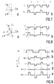
- Fig. 7 shows a phase diagram of a color burst signal without a phase error, and corresponding demodulated U and ⁇ V signals in the demodulation circuit of Fig. 5 during reception of the color burst signal.
- the PAL burst phase diagram of Fig. 7a is identical to that shown in Fig. 3a.
- Fig. 7b shows that the U output of the circuit always has the same sign, while the sign of the demodulated ⁇ V signal before the PAL switch 505 alternates.
- Fig. 8 shows a phase diagram of a color burst signal with a phase error ⁇ and corresponding demodulated U and ⁇ V signals in the demodulation circuit of Fig. 5 during reception of the color burst signal. This results in the U and ⁇ V pulses no longer having a fixed amplitude, but alternatingly the original amplitude ⁇ an error component.
- Fig. 9 shows several signals occurring in the chrominance demodulation circuit of Fig. 5.
- Fig. 9a illustrates the line-alternating switching signal Sw.
- Fig. 9b illustrates the distorted U pulses of Fig. 8b (output of the low-pass filter 501) multiplied by the switching signal Sw as furnished by the multiplier 507.
- the distorted ⁇ V pulses shown in Fig. 9c are identical to those shown in Fig. 8b, which pulses are furnished by the low-pass filter 503.
- Fig. 9d illustrates the sum of the curves of Figs. 9b and 9c, as obtained by the adder 7.
- Fig. 9d contains information about the magnitude of the phase error ⁇ , which after low-pass filtering in low-pass loop filter 9 is used to adjust the VCO 511.
- Fig. 9e illustrates what will happen if the distorted U pulses are multiplied by a switching signal Sw which has the wrong phase because the wrong line number is determined: line-alternating pulses are obtained which have a fixed amplitude containing no information at all about the phase error ⁇ .
Landscapes
- Engineering & Computer Science (AREA)
- Multimedia (AREA)
- Signal Processing (AREA)
- Processing Of Color Television Signals (AREA)
Claims (6)
- Farbhilfsträgerfrequenzregenerationsschaltung mit:einem Burstphasendetektor (1) zum Detektieren der Burstphase eines PAL-Signals mit einer Farbburstfrequenz und einer Zeilenfrequenz, wobei der genannte Burstphasendetektor erste Eingangsmittel aufweist zum Empfangen eines Farbburstsignals (BURST) und zweite Eingangsmittel zum Empfangen von Bezugsdaten (±SIN, COS) mit der genannten Farbburstfrequenz; undeinem Bezugssignalgenerator (11), der mit dem genannten Burstphasendetektor (1) gekoppelt ist zum Liefern der genannten Bezugsdaten (±SIN, COS) zu dem genannten Burstphasendetektor (1), dadurch gekennzeichnet, daß die genannten Bezugsdaten (±SIN, COS) eine Phasen haben, die mit der halben Zeilenfrequenz wechselt, und zwar derart, daß die Bezugsdaten (±SIN, COS) immer eine Phasendifferenz von 90° in bezug auf das Farbburstsignal (BURST) haben.
- Farbartdemodulationsschaltung für ein PAL-Signal mit einer Farbburstperiode, einer Farbburstfrequenz und einer Zeilenfrequenz, wobei diese Farbartdemodulationsschaltung die nachfolgenden Elemente aufweist:dadurch gekennzeichnet, daß ein Vorzeichen des genannten Sinusphasenbezugssignals (-SIB') mit der halben Zeilenfrequenz während der genannten Farbburstperiode wechselt.Mittel (3) zum Multiplizieren eines Eingangssignals mit einem Phasenbezugssignal (-SIN) der genannten Farbburstfrequenz zum Liefern eines ersten Ausgangssignals (U);Mittel (5) zum Multiplizieren des genannten Eingangssignals mit einem Cosinusphasenbezugssignal (COS') mit der genannten Farbburstfrequenz zum Liefern eines zweiten Ausgangssignals (V);Mittel (7) zum Addieren der genannten ersten (U) und der zweiten (V) Ausgangssignale; undMittel (611), die mit den genannten Addiermitteln (7) gekoppelt sind zum Erzeugen des genannten Phasenbezugssignals (-SIN') und des genannten Cosinusphasenbezugssignals (COS'),
- Farbartdemodulationsschaltung für ein PAL-Signal mit einer Farbburstfrequenz und einer Zeilenfrequenz, wobei diese Farbartdemodulationsschaltung die nachfolgenden Elemente aufweist:dadurch gekennzeichnet, daß (±V) der genannten Ausgangssignale (U, ±V) mit einem Schaltsignal (Sw) mit der halben Zeilenfrequenz vor der Addierung (7) mit dem anderen Ausgangssignal (U) multipliziert (507) wird.Mittel (3) zum Multiplizieren eines Eingangssignals mit einem Sinusphasenbezugssignal (-SIN) mit der genannten Farbburstfrequenz zum Liefern eines ersten Ausgangssignals (U);Mittel (5) zum Multiplizieren des genannten Eingangssignals mit einem Cosinusphasenbezugssignal (COS) mit der genannten Farbburstfrequenz zum Liefern eines zweiten Ausgangssignals (±V);Mittel (7) zum Addieren des genannten ersten (U) und zweiten Ausgangssignals; undMittel (511), die mit den genannten Addiermitteln (7) gekoppelt sind zum Erzeugen des genannten Sinusphasenbezugssignals (-SIN) und des genannten Cosinusphasenbezugssignals (COS);
- Empfänger für ein PAL-Videosignal, das ein Farbartsignal aufweist, das einem Farbhilfsträger mit einer Farbhilfsträgerfrequenz aufmoduliert ist, wobei dieser Empfänger eine Farbhilfsträgerfrequenzregenerationsschaltung (1, 9, 11) aufweist, welche die nachfolgenden Elemente aufweist:einen Burstphasendetektor (1) zum Detektieren der Burstphase eines PAL-Signals mit einer Farbburstfrequenz und einer Zeilenfrequenz, wobei der genannte Burstphasendetektor erste Eingangsmittel aufweist zum Empfangen eines Farbburstsignals (BURST) und zweite Eingangsmittel zum Empfangen von Bezugsdaten (±SIN, COS) mit der genannten Farbburstfrequenz; undeinen Bezugssignalgenerator (11), der mit dem genannten Burstphasendetektor (1) gekoppelt ist zum Liefern der genannten Bezugsdaten (±SIN, COS) zu dem genannten Burstphasendetektor (1), dadurch gekennzeichnet, daß die genannten Bezugsdaten (±SIN, COS) eine Phase haben, die mit der halben Zeilenfrequenz derart wechselt, daß die Bezugsdaten (±SIN, COS) immer eine Phasenverschiebung von 90° gegenüber dem Farbburstsignal (BURST) haben.
- Empfänger für ein PAL-Videosignal mit einer Zeilenfrequenz, einer Farbburstperiode, einer Farbburstfrequenz und einem einem Hilfsträger mit der genannten Farbburstfrequenz aufmodulierten Farbartsignal, wobei dieser Empfänger einen Farbartdemodulator (3, 5, 7, 611) aufweist zum Demodulieren des genannten Farbartsignals und mit:dadurch gekennzeichnet, daß ein Vorzeichen des genannten Sinusphasenbezugssignals (-SIN') mit der halben Zeilenfrequenz während der genannten Farbburstperiode wechselt.Mitteln (3) zum Multiplizieren eines Eingangssignals mit einem Sinusphasenbezugssignal (-SIN') mit der genannten Farbburstfrequenz zum Liefern eines ersten Ausgangssignals (U);Mitteln (5) zum Multiplizieren des genannten Eingangssignals mit einem Cosinusphasenbezugssignal (COS') mit der genannten Farbburstfrequenz zum Liefern eines zweiten Ausgangssignals (V);Mitteln (7) zum Addieren des genannten ersten (U) und des genannten zweiten (V) Ausgangssignals; undMitteln (611), die mit den genannten Addiermitteln (7) gekoppelt sind zum Erzeugen des genannten Sinusphasenbezugssignals (-SIN') und des genannten Cosinusphasenbezugssignals (COS');
- Empfänger für ein PAL-Videosignal mit einer Zeilenfrequenz, einer Farbburstfrequenz und einem einem Hilfsträger mit der genannten Farbburstfrequenz aufmodulierten Farbartsignal, wobei dieser Empfänger einen Farbartdemodulator (3, 5, 7, 511) aufweist zum Demodulieren des genannten Farbartsignals und mit:dadurch gekennzeichnet, daß ein Ausgangssignal (±V) der genannten Ausgangssignale (U, ±V) vor Addierung (7) mit dem anderen Ausgangssignal (U) mit einem Schaltsignal (Sw) mit der halben Zeilenfrequenz multipliziert wird.Mitteln (3) zum Multiplizieren eines Eingangssignals mit einem Phasenbezugssignal (-SIN) mit der genannten Farbburstfrequenz zum Liefern eines ersten Ausgangssignals (U);Mitteln (5) zum Multiplizieren des genannten Eingangssignals mit einem Cosinusphasenbezugssignal (COS) mit der genannten Farbburstfrequenz zum Liefern eines zweiten Ausgangssignals (±V);Mitteln (7) zum Addieren des genannten ersten (U) und des genannten zweiten Ausgangssignals; undMitteln (511), die mit den genannten Addiermitteln (7) gekoppelt sind zum Erzeugen des genannten Sinusphasenbezugssignals (-SIN) und des genannten Cosinusphasenbezugssignals (COS);
Priority Applications (1)
| Application Number | Priority Date | Filing Date | Title |
|---|---|---|---|
| EP19930201328 EP0574052B1 (de) | 1992-05-12 | 1993-05-07 | Schaltungsanordnungen zur Farb-Hilfsträger-Frequenzregeneration und zur Farbartdemodulation |
Applications Claiming Priority (3)
| Application Number | Priority Date | Filing Date | Title |
|---|---|---|---|
| EP92201353 | 1992-05-12 | ||
| EP92201353 | 1992-05-12 | ||
| EP19930201328 EP0574052B1 (de) | 1992-05-12 | 1993-05-07 | Schaltungsanordnungen zur Farb-Hilfsträger-Frequenzregeneration und zur Farbartdemodulation |
Publications (2)
| Publication Number | Publication Date |
|---|---|
| EP0574052A1 EP0574052A1 (de) | 1993-12-15 |
| EP0574052B1 true EP0574052B1 (de) | 1998-08-12 |
Family
ID=26131388
Family Applications (1)
| Application Number | Title | Priority Date | Filing Date |
|---|---|---|---|
| EP19930201328 Expired - Lifetime EP0574052B1 (de) | 1992-05-12 | 1993-05-07 | Schaltungsanordnungen zur Farb-Hilfsträger-Frequenzregeneration und zur Farbartdemodulation |
Country Status (1)
| Country | Link |
|---|---|
| EP (1) | EP0574052B1 (de) |
Family Cites Families (4)
| Publication number | Priority date | Publication date | Assignee | Title |
|---|---|---|---|---|
| DE1814836A1 (de) * | 1968-12-14 | 1970-08-13 | Telefunken Patent | Schaltung zur Phasenkorrektur des von einem Aufzeichnungsgeraet entnommenen PAL-Farbtraegers |
| DE2216564C3 (de) * | 1971-04-14 | 1979-09-06 | N.V. Philips' Gloeilampenfabrieken, Eindhoven (Niederlande) | Farbfernsehempfänger-Schaltung zur Gewinnung der richtigen Schaltphase eines Farbartsignals |
| GB1428973A (en) * | 1972-07-20 | 1976-03-24 | Emi Ltd | Circuit arrangements for colour television receivers |
| NL7416457A (nl) * | 1973-12-19 | 1975-06-23 | Indesit | Schakeling voor het verwerken van televisie- -kleursignalen. |
-
1993
- 1993-05-07 EP EP19930201328 patent/EP0574052B1/de not_active Expired - Lifetime
Also Published As
| Publication number | Publication date |
|---|---|
| EP0574052A1 (de) | 1993-12-15 |
Similar Documents
| Publication | Publication Date | Title |
|---|---|---|
| US4745463A (en) | Generalized chrominance signal demodulator for a sampled data television signal processing system | |
| US5506636A (en) | HDTV signal receiver with imaginary-sample-presence detector for QAM/VSB mode selection | |
| US5715012A (en) | Radio receivers for receiving both VSB and QAM digital HDTV signals | |
| GB2059711A (en) | Digital demodulation or modulation of television chrominance signals | |
| EP0340648B1 (de) | Schaltung zur Verbesserung der Bildqualität | |
| US5410573A (en) | Digital phase-locked loop circuit | |
| US4970469A (en) | Phase detector and frequency demodulator including such a phase detector | |
| US6034735A (en) | Clock generator for digital video signal processing apparatus | |
| US5170131A (en) | Demodulator for demodulating digital signal modulated by minimum shift keying and method therefor | |
| US8040158B2 (en) | Frequency difference detection apparatus and method, frequency discrimination apparatus and method, and frequency synthesis apparatus and method | |
| US4095187A (en) | Demodulation system for a multi-level multi-phase superposition-modulated carrier wave | |
| US4686569A (en) | Circuitry for reducing demodulation phase error as for an automatic deghosting system | |
| US4740759A (en) | Angle demodulator with second order interference prevention | |
| JP2001095005A (ja) | クロック発生回路 | |
| EP0574052A1 (de) | Schaltungsanordnungen zur Farb-Hilfsträger-Frequenzregeneration und zur Farbartdemodulation | |
| US5440349A (en) | Color signal demodulation circuit and method therefor | |
| JPH11285020A (ja) | 色信号復調回路 | |
| US5757439A (en) | Method for detecting color burst signal amplitude for chrominance signal level control and an apparatus therefor | |
| JP3411328B2 (ja) | 色副搬送波周波数の再生及びクロミナンス復調 | |
| EP0160531B1 (de) | Demodulatorschaltungen für amplitudenmodulierte Signale | |
| US5526061A (en) | Circuit arrangement for demodulating a video signal | |
| US4578706A (en) | Television synchronous receiver | |
| US5648823A (en) | Circuit configuration for intermediate frequency demodulation and device for video signal processing including the circuit | |
| JP3399017B2 (ja) | 位相同期装置 | |
| JP2572986B2 (ja) | 復調回路 |
Legal Events
| Date | Code | Title | Description |
|---|---|---|---|
| PUAI | Public reference made under article 153(3) epc to a published international application that has entered the european phase |
Free format text: ORIGINAL CODE: 0009012 |
|
| AK | Designated contracting states |
Kind code of ref document: A1 Designated state(s): DE FR GB IT |
|
| 17P | Request for examination filed |
Effective date: 19940530 |
|
| 17Q | First examination report despatched |
Effective date: 19960712 |
|
| GRAG | Despatch of communication of intention to grant |
Free format text: ORIGINAL CODE: EPIDOS AGRA |
|
| GRAG | Despatch of communication of intention to grant |
Free format text: ORIGINAL CODE: EPIDOS AGRA |
|
| GRAG | Despatch of communication of intention to grant |
Free format text: ORIGINAL CODE: EPIDOS AGRA |
|
| GRAH | Despatch of communication of intention to grant a patent |
Free format text: ORIGINAL CODE: EPIDOS IGRA |
|
| GRAH | Despatch of communication of intention to grant a patent |
Free format text: ORIGINAL CODE: EPIDOS IGRA |
|
| GRAA | (expected) grant |
Free format text: ORIGINAL CODE: 0009210 |
|
| AK | Designated contracting states |
Kind code of ref document: B1 Designated state(s): DE FR GB IT |
|
| RAP4 | Party data changed (patent owner data changed or rights of a patent transferred) |
Owner name: KONINKLIJKE PHILIPS ELECTRONICS N.V. |
|
| REF | Corresponds to: |
Ref document number: 69320261 Country of ref document: DE Date of ref document: 19980917 |
|
| ET | Fr: translation filed | ||
| PLBE | No opposition filed within time limit |
Free format text: ORIGINAL CODE: 0009261 |
|
| STAA | Information on the status of an ep patent application or granted ep patent |
Free format text: STATUS: NO OPPOSITION FILED WITHIN TIME LIMIT |
|
| 26N | No opposition filed | ||
| REG | Reference to a national code |
Ref country code: GB Ref legal event code: IF02 |
|
| REG | Reference to a national code |
Ref country code: FR Ref legal event code: D6 |
|
| REG | Reference to a national code |
Ref country code: GB Ref legal event code: 746 Effective date: 20021107 |
|
| PGFP | Annual fee paid to national office [announced via postgrant information from national office to epo] |
Ref country code: FR Payment date: 20030526 Year of fee payment: 11 |
|
| PGFP | Annual fee paid to national office [announced via postgrant information from national office to epo] |
Ref country code: GB Payment date: 20030529 Year of fee payment: 11 |
|
| PGFP | Annual fee paid to national office [announced via postgrant information from national office to epo] |
Ref country code: DE Payment date: 20030715 Year of fee payment: 11 |
|
| PG25 | Lapsed in a contracting state [announced via postgrant information from national office to epo] |
Ref country code: GB Free format text: LAPSE BECAUSE OF NON-PAYMENT OF DUE FEES Effective date: 20040507 |
|
| PG25 | Lapsed in a contracting state [announced via postgrant information from national office to epo] |
Ref country code: DE Free format text: LAPSE BECAUSE OF NON-PAYMENT OF DUE FEES Effective date: 20041201 |
|
| GBPC | Gb: european patent ceased through non-payment of renewal fee |
Effective date: 20040507 |
|
| PG25 | Lapsed in a contracting state [announced via postgrant information from national office to epo] |
Ref country code: FR Free format text: LAPSE BECAUSE OF NON-PAYMENT OF DUE FEES Effective date: 20050131 |
|
| REG | Reference to a national code |
Ref country code: FR Ref legal event code: ST |
|
| PG25 | Lapsed in a contracting state [announced via postgrant information from national office to epo] |
Ref country code: IT Free format text: LAPSE BECAUSE OF NON-PAYMENT OF DUE FEES;WARNING: LAPSES OF ITALIAN PATENTS WITH EFFECTIVE DATE BEFORE 2007 MAY HAVE OCCURRED AT ANY TIME BEFORE 2007. THE CORRECT EFFECTIVE DATE MAY BE DIFFERENT FROM THE ONE RECORDED. Effective date: 20050507 |