EP0574207A2 - Circuit imprimé multicouche et sa méthode de fabrication - Google Patents
Circuit imprimé multicouche et sa méthode de fabrication Download PDFInfo
- Publication number
- EP0574207A2 EP0574207A2 EP93304382A EP93304382A EP0574207A2 EP 0574207 A2 EP0574207 A2 EP 0574207A2 EP 93304382 A EP93304382 A EP 93304382A EP 93304382 A EP93304382 A EP 93304382A EP 0574207 A2 EP0574207 A2 EP 0574207A2
- Authority
- EP
- European Patent Office
- Prior art keywords
- printed circuit
- substrate
- circuit board
- multilayer printed
- hybrid module
- Prior art date
- Legal status (The legal status is an assumption and is not a legal conclusion. Google has not performed a legal analysis and makes no representation as to the accuracy of the status listed.)
- Withdrawn
Links
Images


Classifications
-
- H—ELECTRICITY
- H05—ELECTRIC TECHNIQUES NOT OTHERWISE PROVIDED FOR
- H05K—PRINTED CIRCUITS; CASINGS OR CONSTRUCTIONAL DETAILS OF ELECTRIC APPARATUS; MANUFACTURE OF ASSEMBLAGES OF ELECTRICAL COMPONENTS
- H05K1/00—Printed circuits
- H05K1/18—Printed circuits structurally associated with non-printed electric components
- H05K1/182—Printed circuits structurally associated with non-printed electric components associated with components mounted in printed circuit boards [PCB], e.g. insert-mounted components [IMC]
- H05K1/185—Printed circuits structurally associated with non-printed electric components associated with components mounted in printed circuit boards [PCB], e.g. insert-mounted components [IMC] associated with components encapsulated in the insulating substrate of the PCBs; associated with components incorporated in internal layers of multilayer circuit boards
-
- H—ELECTRICITY
- H10—SEMICONDUCTOR DEVICES; ELECTRIC SOLID-STATE DEVICES NOT OTHERWISE PROVIDED FOR
- H10W—GENERIC PACKAGES, INTERCONNECTIONS, CONNECTORS OR OTHER CONSTRUCTIONAL DETAILS OF DEVICES COVERED BY CLASS H10
- H10W70/00—Package substrates; Interposers; Redistribution layers [RDL]
- H10W70/01—Manufacture or treatment
- H10W70/05—Manufacture or treatment of insulating or insulated package substrates, or of interposers, or of redistribution layers
- H10W70/093—Connecting or disconnecting other interconnections thereto or therefrom, e.g. connecting bond wires or bumps
-
- H—ELECTRICITY
- H10—SEMICONDUCTOR DEVICES; ELECTRIC SOLID-STATE DEVICES NOT OTHERWISE PROVIDED FOR
- H10W—GENERIC PACKAGES, INTERCONNECTIONS, CONNECTORS OR OTHER CONSTRUCTIONAL DETAILS OF DEVICES COVERED BY CLASS H10
- H10W70/00—Package substrates; Interposers; Redistribution layers [RDL]
- H10W70/60—Insulating or insulated package substrates; Interposers; Redistribution layers
-
- H—ELECTRICITY
- H05—ELECTRIC TECHNIQUES NOT OTHERWISE PROVIDED FOR
- H05K—PRINTED CIRCUITS; CASINGS OR CONSTRUCTIONAL DETAILS OF ELECTRIC APPARATUS; MANUFACTURE OF ASSEMBLAGES OF ELECTRICAL COMPONENTS
- H05K2201/00—Indexing scheme relating to printed circuits covered by H05K1/00
- H05K2201/03—Conductive materials
- H05K2201/0332—Structure of the conductor
- H05K2201/0335—Layered conductors or foils
- H05K2201/0355—Metal foils
-
- H—ELECTRICITY
- H05—ELECTRIC TECHNIQUES NOT OTHERWISE PROVIDED FOR
- H05K—PRINTED CIRCUITS; CASINGS OR CONSTRUCTIONAL DETAILS OF ELECTRIC APPARATUS; MANUFACTURE OF ASSEMBLAGES OF ELECTRICAL COMPONENTS
- H05K2201/00—Indexing scheme relating to printed circuits covered by H05K1/00
- H05K2201/09—Shape and layout
- H05K2201/09209—Shape and layout details of conductors
- H05K2201/095—Conductive through-holes or vias
- H05K2201/09509—Blind vias, i.e. vias having one side closed
-
- H—ELECTRICITY
- H05—ELECTRIC TECHNIQUES NOT OTHERWISE PROVIDED FOR
- H05K—PRINTED CIRCUITS; CASINGS OR CONSTRUCTIONAL DETAILS OF ELECTRIC APPARATUS; MANUFACTURE OF ASSEMBLAGES OF ELECTRICAL COMPONENTS
- H05K2201/00—Indexing scheme relating to printed circuits covered by H05K1/00
- H05K2201/10—Details of components or other objects attached to or integrated in a printed circuit board
- H05K2201/10613—Details of electrical connections of non-printed components, e.g. special leads
- H05K2201/10621—Components characterised by their electrical contacts
- H05K2201/10674—Flip chip
-
- H—ELECTRICITY
- H05—ELECTRIC TECHNIQUES NOT OTHERWISE PROVIDED FOR
- H05K—PRINTED CIRCUITS; CASINGS OR CONSTRUCTIONAL DETAILS OF ELECTRIC APPARATUS; MANUFACTURE OF ASSEMBLAGES OF ELECTRICAL COMPONENTS
- H05K2201/00—Indexing scheme relating to printed circuits covered by H05K1/00
- H05K2201/10—Details of components or other objects attached to or integrated in a printed circuit board
- H05K2201/10613—Details of electrical connections of non-printed components, e.g. special leads
- H05K2201/10954—Other details of electrical connections
- H05K2201/10969—Metallic case or integral heatsink of component electrically connected to a pad on PCB
-
- H—ELECTRICITY
- H05—ELECTRIC TECHNIQUES NOT OTHERWISE PROVIDED FOR
- H05K—PRINTED CIRCUITS; CASINGS OR CONSTRUCTIONAL DETAILS OF ELECTRIC APPARATUS; MANUFACTURE OF ASSEMBLAGES OF ELECTRICAL COMPONENTS
- H05K3/00—Apparatus or processes for manufacturing printed circuits
- H05K3/46—Manufacturing multilayer circuits
- H05K3/4644—Manufacturing multilayer circuits by building the multilayer layer by layer, i.e. build-up multilayer circuits
- H05K3/4652—Adding a circuit layer by laminating a metal foil or a preformed metal foil pattern
-
- H—ELECTRICITY
- H10—SEMICONDUCTOR DEVICES; ELECTRIC SOLID-STATE DEVICES NOT OTHERWISE PROVIDED FOR
- H10W—GENERIC PACKAGES, INTERCONNECTIONS, CONNECTORS OR OTHER CONSTRUCTIONAL DETAILS OF DEVICES COVERED BY CLASS H10
- H10W72/00—Interconnections or connectors in packages
- H10W72/01—Manufacture or treatment
- H10W72/0198—Manufacture or treatment batch processes
-
- H—ELECTRICITY
- H10—SEMICONDUCTOR DEVICES; ELECTRIC SOLID-STATE DEVICES NOT OTHERWISE PROVIDED FOR
- H10W—GENERIC PACKAGES, INTERCONNECTIONS, CONNECTORS OR OTHER CONSTRUCTIONAL DETAILS OF DEVICES COVERED BY CLASS H10
- H10W72/00—Interconnections or connectors in packages
- H10W72/851—Dispositions of multiple connectors or interconnections
- H10W72/874—On different surfaces
-
- H—ELECTRICITY
- H10—SEMICONDUCTOR DEVICES; ELECTRIC SOLID-STATE DEVICES NOT OTHERWISE PROVIDED FOR
- H10W—GENERIC PACKAGES, INTERCONNECTIONS, CONNECTORS OR OTHER CONSTRUCTIONAL DETAILS OF DEVICES COVERED BY CLASS H10
- H10W72/00—Interconnections or connectors in packages
- H10W72/90—Bond pads, in general
- H10W72/941—Dispositions of bond pads
- H10W72/9413—Dispositions of bond pads on encapsulations
-
- H—ELECTRICITY
- H10—SEMICONDUCTOR DEVICES; ELECTRIC SOLID-STATE DEVICES NOT OTHERWISE PROVIDED FOR
- H10W—GENERIC PACKAGES, INTERCONNECTIONS, CONNECTORS OR OTHER CONSTRUCTIONAL DETAILS OF DEVICES COVERED BY CLASS H10
- H10W90/00—Package configurations
- H10W90/701—Package configurations characterised by the relative positions of pads or connectors relative to package parts
- H10W90/731—Package configurations characterised by the relative positions of pads or connectors relative to package parts of die-attach connectors
- H10W90/734—Package configurations characterised by the relative positions of pads or connectors relative to package parts of die-attach connectors between a chip and a stacked insulating package substrate, interposer or RDL
Definitions
- the present invention relates to a multilayer printed circuit board and a method for manufacturing the same. More particularly, the present invention is concerned with a multilayer printed circuit board having a structure such that electronic components are buried in the board so that the board can have an increased volume of electronic components disposed therein, and a method for manufacturing such a multilayer printed circuit board.
- a multilayer printed circuit board comprising a plurality of printed circuit substrates is used in various apparatus, such as data processing machines, electronic business machines and home appliances, in which a high integration of circuits is required.
- the high integration of circuits is ensured by the use of connection holes, such as blind via-holes and interstitial via-holes, which mutually electrically connect the circuits included in the board.
- connection holes such as blind via-holes and interstitial via-holes
- the multilayer printed circuit board can have a large volume of electronic component mounted thereon.
- the volume of electronic components mounted on the multilayer printed circuit board there is still a strong demand for a further increase in the volume of electronic components mounted on the multilayer printed circuit board.
- an object of the present invention to provide a multilayer printed circuit board having an increased volume of electronic components disposed therein.
- a multilayer printed circuit board comprising an inner printed circuit substrate having a hybrid module with electronic component functions die-bonded thereto and at least one outer printed circuit substrate laminated to said inner printed circuit substrate so that said hybrid module is sandwiched between said inner printed circuit substrate and said outer printed circuit substrate.
- a method for manufacturing a multilayer printed circuit board comprising the steps of:
- the thus manufactured multilayer printed circuit board assumes a structure such that a hybrid module having electronic component functions or electronic component network functions is sandwiched between printed circuit substrates, so that the condition arises that the electronic component or electronic circuit functions are buried in the layered printed circuit board. Due to this burying of the electronic component or electronic circuit functions in addition to the mounting of electronic components on the outer surfaces of the substrate laminate, the multilayer printed circuit board of the present invention can have an increased volume of electronic components disposed therein.
- the multilayer printed circuit board provided with electronic component or electronic circuit functions is effectively manufactured by the method of the present invention, in which a hybrid module is die-bonded to an inner substrate, followed by lamination of at least one outer substrate, then connection holes are formed in the outer substrate, and thereafter the outer substrate is electrically connected to the hybrid module through the connection holes.
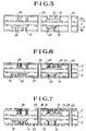
- Fig. 1 shows a sequence of steps to be taken in the manufacturing method according to one embodiment of the present invention.
- Figs. 2 to 8 show sectional views of respective articles produced in the steps.
- a four conductor layer printed circuit board is described, comprising an inner substrate 1 and, laminated to an upper surface and a lower surface of the inner substrate 1, two outer substrates 2, 3.
- a first circuit conductor is formed on the upper surface of the upper outer substrate 2
- a second circuit conductor formed on the upper surface of the inner substrate 1
- a third circuit conductor formed on the lower surface of the inner substrate land a fourth circuit conductor formed on the lower surface of the lower outer substrate 3.
- a substrate having both sides thereof clad with a copper foil is provided, and the copper foils are subjected to a treatment comprising application of a photosensitive resin, light exposure and etching for forming a pattern comprising e.g., a circuit 11, a land 12 and a bonding land 13, on both of the sides of the substrate, thereby obtaining an inner substrate 1, as illustrated in Fig. 2.
- the inner substrate 1 is surface treated, and hybrid modules 14, 15 are die-bonded to the bonding lands 13 of the inner substrate 1, as illustrated in Fig. 3.
- the die-bonding of the hybrid modules 14, 15 to respective bonding lands 13 is performed through a conductive or a non-conductive adhesive.
- Each of the hybrid modules has electronic component functions. For example, it is selected from a module comprising a ceramic substrate and, disposed thereon or therein, a passive component, such as a resistor and a capacitor; a module comprising a ceramic substrate and, disposed thereon or therein, an active component, such as a transistor, a diode, an IC or an LSI; and a module comprising a ceramic substrate and, disposed thereon or therein, a passive component in combination with an active component.
- the hybrid module comprises a ceramic substrate and, disposed thereon or therein, a circuit formed of passive and active components electrically connected in a network fashion.
- the hybrid module has lands (not shown) for electrically connecting these passive and active components with circuits on the inner substrate 1 and the outer substrates 2, 3.
- the above-mentioned lands are formed by plating of copper, its alloy or other conductive metals.
- a hybrid module is sandwiched between the inner substrate 1 and the outer substrate, 2, 3. It is preferred that the thickness of such a hybrid module be small.
- the hybrid module 14 is a circuit module including a plurality of passive components, such as a resistor and a capacitor, electrically connected with each other and arranged in an array fashion, while the other hybrid module 15 is a module including a semiconductor chip.
- Fig. 4 illustrates a structure obtained by laminating outer substrates 2, 3 to an upper surface and a lower surface, respectively, of the inner substrate 1 after the die-bonding of the hybrid modules 14, 15 to the inner substrate 1.
- the lamination of the outer substrates 2, 3 is generally performed by pressing, roll lamination and/or an adhesive.
- the outer substrates 2, 3 respectively comprise insulating layers 2a, 3a which are, on one side thereof, clad with copper foils 2b, 3b, respectively.
- the respective copper foils 2b, 3b are subjected to a treatment comprising application of a photosensitive resin, light exposure and etching for pattern formation.
- the insulating layers 2a, 3a are partially removed by chemical dissolution or laser irradiation at portions corresponding to portions of the copper foils 2b, 3b removed as a result of the above-mentioned treatment for pattern formation, thereby forming connection holes as shown in Fig. 5.
- Fig. 5 illustrates a structure in which the connection holes have been formed in the outer substrates 2, 3.
- the connection holes are at least formed at portions corresponding to lands of the hybrid modules 14, 15.
- a connection hole 21 corresponds to a land of the hybrid module 14 disposed on the upper side of the inner substrate 1.
- a connection hole 22 corresponds to a land of the hybrid module 14 disposed on the lower side of the inner substrate 1.
- a connection hole 23 corresponds to a land of the hybrid module 15.
- numeral 24 designates a connection hole formed at a portion corresponding to a land 12 of the inner substrate 1.
- Numeral 25 designates a connection hole formed so as to pass through the laminated substrates 1, 2, 3.
- connection hole 24 is a blind via-hole for electrically connecting the land 12 of the inner substrate 1 with a land of the upper outer substrate 2.
- the connection hole 25 is a through-hole for electrically connecting the land 12 of the inner substrate 1 with lands of the upper and lower outer substrates 2, 3.
- the connection hole 25 as a through-hole is preferably formed by a drill or a punch.
- connection holes 21, 22, 23, 24, 25 the resultant preliminary multilayer printed circuit board is subjected to plating treatment, such as electroless plating and electrolytic plating, so that the outer surfaces of the upper and lower outer substrates 2, 3 and the inner surfaces of the connection holes 21, 22, 23, 24, 25 are plated to form a plating layer 27 adhering thereto, as shown in Fig. 6.
- plating treatment such as electroless plating and electrolytic plating
- the lands of the hybrid modules 14, 15 are electrically connected with lands of the outer substrates 2, 3, and the connection holes 24, 25 become a blind via-hole and a through-hole, respectively.
- the hybrid modules 14, 15 are electrically connected with the outer substrates 2, 3, so that while being buried in the laminated substrates, the hybrid modules 14, 15 can function as an electronic component or an electronic circuit including electronic components electrically connected in a network fashion.
- the copper foils 2b, 3b of the outer substrates 2, 3 and the plating layer 27 formed on the copper foils 2b, 3b are subjected to a treatment comprising application of a photosensitive resin, light exposure and etching for pattern formation to form a circuit 29 and lands on the outer substrates 2, 3.
- numeral 30 designates a land for electrically connecting the inner substrate 1 and the outer substrates 2, 3.
- a land 31 is one for electrically connecting the hybrid modules 14, 15 with the outer substrates 2, 3.
- a solder resist 35 is applied to the outer surfaces of the outer substrate 2, 3 to thereby obtain a multilayer printed circuit board as shown in Fig. 8.
- the hybrid modules 14, 15 are sandwiched between the inner substrate 1 and the outer substrates 2, 3 and are electrically connected with the inner substrate 1 and the outer substrates, so that a structure results such that desired electronic components or a desired electronic circuit including electronic components is buried in the laminated substrate board. Due to this burial of electronic components in addition to the mounting of electronic components on the outer surfaces of a multilayer printed circuit board, the packaging density of electronic components can be remarkably increased in the multilayer printed circuit board of the present invention.
- the electric connection of the hybrid modules 14, 15 to the outer substrates 2, 3 can be performed concurrently with the formation of circuits and lands on the outer substrates 2, 3, operations for connection, such as wire bonding, become unnecessary and the electric connection can be performed at high efficiency with high precision.
- the hybrid modules 14, 15 buried in the multilayer printed circuit board are connected via the plating layer 27 to lands of the outer substrates 2, 3, heat conduction is effectively performed to ensure excellent heat radiation efficiency and hence operations not adversely affected by temperatures.
- the hybrid modules 14, 15 are individually sandwiched between the copper foils of the inner substrate 1 and those of the outer substrates 2, 3, electromagnetic wave shield is ensured to thereby minimize noise.
- the multilayer printed circuit board of the present invention may be comprised of two printed circuit substrates or of four or more printed circuit substrates.
- the electric connection of the hybrid modules to the outer substrates may be performed through connection holes filled with a conductor paste.
- the hybrid modules are not limited to a module comprising a ceramic substrate and, disposed thereon, electronic components. Further, an electronic component, such as a semiconductor chip, per se may be die-bonded as a hybrid module to the inner substrate.
- a hybrid module having electronic component or electronic circuit functions is buried in the printed circuit board and desirable electric connection is performed therefor, so that the packaging density of electronic components can be increased. Further, since the electric connection of the hybrid module to the printed circuit substrate can be performed concurrently with the manufacturing of the multilayer printed circuit board, the electric connection can be effectively made with high precision.
Landscapes
- Engineering & Computer Science (AREA)
- Microelectronics & Electronic Packaging (AREA)
- Manufacturing & Machinery (AREA)
- Production Of Multi-Layered Print Wiring Board (AREA)
- Combinations Of Printed Boards (AREA)
Applications Claiming Priority (2)
| Application Number | Priority Date | Filing Date | Title |
|---|---|---|---|
| JP04173798A JP3086332B2 (ja) | 1992-06-08 | 1992-06-08 | 多層プリント配線板の製造方法 |
| JP173798/92 | 1992-06-08 |
Publications (2)
| Publication Number | Publication Date |
|---|---|
| EP0574207A2 true EP0574207A2 (fr) | 1993-12-15 |
| EP0574207A3 EP0574207A3 (fr) | 1994-01-12 |
Family
ID=15967358
Family Applications (1)
| Application Number | Title | Priority Date | Filing Date |
|---|---|---|---|
| EP19930304382 Withdrawn EP0574207A3 (fr) | 1992-06-08 | 1993-06-04 | Circuit imprimé multicouche et sa méthode de fabrication |
Country Status (3)
| Country | Link |
|---|---|
| EP (1) | EP0574207A3 (fr) |
| JP (1) | JP3086332B2 (fr) |
| KR (1) | KR940001773A (fr) |
Cited By (3)
| Publication number | Priority date | Publication date | Assignee | Title |
|---|---|---|---|---|
| US7068519B2 (en) | 1997-11-25 | 2006-06-27 | Matsushita Electric Industrial Co., Ltd. | Printed circuit board and method manufacturing the same |
| WO2006056648A3 (fr) * | 2004-11-26 | 2006-08-31 | Imbera Electronics Oy | Module electronique et procede de fabrication associe |
| WO2007003414A1 (fr) | 2005-07-04 | 2007-01-11 | Schweizer Electronic Ag | Structure multicouche de plaquettes ayant un composant electrique integre, et son procede de production |
Families Citing this family (6)
| Publication number | Priority date | Publication date | Assignee | Title |
|---|---|---|---|---|
| JP4851652B2 (ja) * | 2000-02-09 | 2012-01-11 | 日本特殊陶業株式会社 | 配線基板及びその製造方法 |
| JP2002111222A (ja) * | 2000-10-02 | 2002-04-12 | Matsushita Electric Ind Co Ltd | 多層基板 |
| KR100867038B1 (ko) * | 2005-03-02 | 2008-11-04 | 삼성전기주식회사 | 커패시터 내장형 인쇄회로기판 및 그 제조방법 |
| KR100716824B1 (ko) * | 2005-04-28 | 2007-05-09 | 삼성전기주식회사 | 하이브리드 재료를 이용한 커패시터 내장형 인쇄회로기판및 그 제조방법 |
| JP2007335675A (ja) * | 2006-06-15 | 2007-12-27 | Fuji Electric Systems Co Ltd | 電源装置および電源装置の製造方法 |
| JP2007165932A (ja) * | 2007-02-22 | 2007-06-28 | Matsushita Electric Ind Co Ltd | 多層基板 |
Family Cites Families (3)
| Publication number | Priority date | Publication date | Assignee | Title |
|---|---|---|---|---|
| USH416H (en) * | 1981-08-31 | 1988-01-05 | Rogers Corporation | High capacitance flexible circuit |
| JPH01207992A (ja) * | 1988-02-16 | 1989-08-21 | Hitachi Ltd | 回路配線板 |
| JPH02164096A (ja) * | 1988-12-19 | 1990-06-25 | Matsushita Electric Ind Co Ltd | 多層電子回路基板とその製造方法 |
-
1992
- 1992-06-08 JP JP04173798A patent/JP3086332B2/ja not_active Expired - Fee Related
- 1992-06-18 KR KR1019930010533A patent/KR940001773A/ko not_active Ceased
-
1993
- 1993-06-04 EP EP19930304382 patent/EP0574207A3/fr not_active Withdrawn
Cited By (6)
| Publication number | Priority date | Publication date | Assignee | Title |
|---|---|---|---|---|
| US7068519B2 (en) | 1997-11-25 | 2006-06-27 | Matsushita Electric Industrial Co., Ltd. | Printed circuit board and method manufacturing the same |
| WO2006056648A3 (fr) * | 2004-11-26 | 2006-08-31 | Imbera Electronics Oy | Module electronique et procede de fabrication associe |
| US8547701B2 (en) | 2004-11-26 | 2013-10-01 | Imbera Electronics Oy | Electronics module and method for manufacturing the same |
| WO2007003414A1 (fr) | 2005-07-04 | 2007-01-11 | Schweizer Electronic Ag | Structure multicouche de plaquettes ayant un composant electrique integre, et son procede de production |
| CN101258787B (zh) * | 2005-07-04 | 2011-02-09 | 施韦策电子公司 | 带有集成电器件的印刷电路板多层结构和制造方法 |
| US8072768B2 (en) | 2005-07-04 | 2011-12-06 | Schweizer Electronic Ag | Multilayer printed circuit board structure comprising an integrated electrical component, and production method therefor |
Also Published As
| Publication number | Publication date |
|---|---|
| KR940001773A (ko) | 1994-01-11 |
| EP0574207A3 (fr) | 1994-01-12 |
| JPH05343856A (ja) | 1993-12-24 |
| JP3086332B2 (ja) | 2000-09-11 |
Similar Documents
| Publication | Publication Date | Title |
|---|---|---|
| US6930257B1 (en) | Integrated circuit substrate having laminated laser-embedded circuit layers | |
| JP4339739B2 (ja) | 部品内蔵型多層基板 | |
| US7345888B2 (en) | Component built-in wiring board and manufacturing method of component built-in wiring board | |
| US7282394B2 (en) | Printed circuit board including embedded chips and method of fabricating the same using plating | |
| EP0609774B1 (fr) | Plaquette ou carte à circuit imprimé pour le montage direct de puces et sa fabrication | |
| EP1060647B1 (fr) | Procede de fabrication de modules multi-fonctions hyperfrequence a l'aide de substrats composites de fluoropolymeres | |
| US6861284B2 (en) | Semiconductor device and production method thereof | |
| US6711812B1 (en) | Method of making metal core substrate printed circuit wiring board enabling thermally enhanced ball grid array (BGA) packages | |
| JP3577421B2 (ja) | 半導体装置用パッケージ | |
| US6713792B2 (en) | Integrated circuit heat sink device including through hole to facilitate communication | |
| EP0574206A2 (fr) | Circuit imprimé multicouche et sa méthode de fabrication | |
| JP2001298273A (ja) | 電子部品内蔵実装基板及びそれを用いた半導体パッケージ | |
| EP0574207A2 (fr) | Circuit imprimé multicouche et sa méthode de fabrication | |
| SG174088A1 (en) | Circuit board | |
| US8826531B1 (en) | Method for making an integrated circuit substrate having laminated laser-embedded circuit layers | |
| US20030042224A1 (en) | Method for preparing ball grid array board | |
| US6586687B2 (en) | Printed wiring board with high density inner layer structure | |
| JP3179572B2 (ja) | 多層プリント配線板およびその製造方法 | |
| JP2006165242A (ja) | プリント配線板およびその製造方法 | |
| JP2001308484A (ja) | 回路基板及びその製造方法 | |
| JP2784524B2 (ja) | 多層電子部品搭載用基板及びその製造法 | |
| JP3179564B2 (ja) | 多層プリント配線板およびその製造方法 | |
| KR100477258B1 (ko) | 범프의 형성방법 및 이로부터 형성된 범프를 이용한인쇄회로기판의 제조방법 | |
| KR20030071391A (ko) | 범프의 형성방법 및 이로부터 형성된 범프를 이용한인쇄회로기판의 제조방법 | |
| KR100649683B1 (ko) | 무선고주파용 인쇄회로기판 및 그 제조방법 |
Legal Events
| Date | Code | Title | Description |
|---|---|---|---|
| PUAI | Public reference made under article 153(3) epc to a published international application that has entered the european phase |
Free format text: ORIGINAL CODE: 0009012 |
|
| PUAL | Search report despatched |
Free format text: ORIGINAL CODE: 0009013 |
|
| 17P | Request for examination filed |
Effective date: 19930612 |
|
| AK | Designated contracting states |
Kind code of ref document: A2 Designated state(s): BE DE ES FR GB IT NL SE |
|
| AK | Designated contracting states |
Kind code of ref document: A3 Designated state(s): BE DE ES FR GB IT NL SE |
|
| STAA | Information on the status of an ep patent application or granted ep patent |
Free format text: STATUS: THE APPLICATION HAS BEEN WITHDRAWN |
|
| 18W | Application withdrawn |
Withdrawal date: 19940704 |
|
| R18W | Application withdrawn (corrected) |
Effective date: 19940704 |