EP0574329A1 - Empfänger der Überabtastung zur Beseitigung von Störimpulsen verwendet - Google Patents
Empfänger der Überabtastung zur Beseitigung von Störimpulsen verwendet Download PDFInfo
- Publication number
- EP0574329A1 EP0574329A1 EP93420169A EP93420169A EP0574329A1 EP 0574329 A1 EP0574329 A1 EP 0574329A1 EP 93420169 A EP93420169 A EP 93420169A EP 93420169 A EP93420169 A EP 93420169A EP 0574329 A1 EP0574329 A1 EP 0574329A1
- Authority
- EP
- European Patent Office
- Prior art keywords
- signals
- digital
- samples
- state
- filtering
- Prior art date
- Legal status (The legal status is an assumption and is not a legal conclusion. Google has not performed a legal analysis and makes no representation as to the accuracy of the status listed.)
- Ceased
Links
- 238000001914 filtration Methods 0.000 claims abstract description 21
- 244000045947 parasite Species 0.000 claims description 21
- 238000004458 analytical method Methods 0.000 claims description 20
- 238000005070 sampling Methods 0.000 claims description 6
- 238000001514 detection method Methods 0.000 abstract description 11
- 230000000630 rising effect Effects 0.000 abstract description 8
- 238000004891 communication Methods 0.000 abstract description 6
- 230000005540 biological transmission Effects 0.000 description 8
- 230000007704 transition Effects 0.000 description 5
- 238000003708 edge detection Methods 0.000 description 3
- 230000001360 synchronised effect Effects 0.000 description 3
- 238000010586 diagram Methods 0.000 description 2
- 230000003071 parasitic effect Effects 0.000 description 2
- 239000003990 capacitor Substances 0.000 description 1
- 230000008878 coupling Effects 0.000 description 1
- 238000010168 coupling process Methods 0.000 description 1
- 238000005859 coupling reaction Methods 0.000 description 1
- 230000007547 defect Effects 0.000 description 1
- 230000004069 differentiation Effects 0.000 description 1
- 238000010616 electrical installation Methods 0.000 description 1
- 230000005674 electromagnetic induction Effects 0.000 description 1
- 230000008030 elimination Effects 0.000 description 1
- 238000003379 elimination reaction Methods 0.000 description 1
- 230000006870 function Effects 0.000 description 1
- 238000005259 measurement Methods 0.000 description 1
- 238000001228 spectrum Methods 0.000 description 1
- 230000001052 transient effect Effects 0.000 description 1
Images
Classifications
-
- H—ELECTRICITY
- H04—ELECTRIC COMMUNICATION TECHNIQUE
- H04L—TRANSMISSION OF DIGITAL INFORMATION, e.g. TELEGRAPHIC COMMUNICATION
- H04L25/00—Baseband systems
- H04L25/02—Details ; arrangements for supplying electrical power along data transmission lines
- H04L25/06—DC level restoring means; Bias distortion correction ; Decision circuits providing symbol by symbol detection
- H04L25/068—DC level restoring means; Bias distortion correction ; Decision circuits providing symbol by symbol detection by sampling faster than the nominal bit rate
Definitions
- the invention relates to a device for receiving digital signals comprising input means providing output signals representative of the logic state of the digital signals applied to the input of the receiving device, a processing circuit and filtering means. parasites.
- the connections between electronic devices in disturbed industrial environments are often carried out by transmission lines which convey digital information in serial or parallel form.
- the lines can be in synchronous or asynchronous mode.
- it is known to shield the connections by the use of special cables whose shielding is earthed to the general ground of the electrical installation or to earth.
- high energy signals may reach the receiver.
- Clipping devices that eliminate overvoltages to protect electronic components, and analog filters, made with RC or LR cells, help reduce unwanted interference.
- These disturbed connections are for example close to high current or high voltage cut-off devices such as circuit breakers or switches.
- the object of the invention is a digital filtering device making it possible to eliminate the parasites present on the signals carrying the information.
- the filtering means comprise digital filtering means connected between the input means and the processing circuit, the digital filtering means comprising means for sampling the signals of output of the input means and of the analysis means, during a period of analysis of a first predetermined number of successive samples, the analysis means comprising means of determining the number of samples having a first logic state during the analysis period, so as to output a signal or first logical state if the number of samples in this state is greater than a predetermined value.
- the invention comprises a plurality of filtering means having different first numbers and different predetermined values. In this way, it is possible to apply different filtering criteria for edge detection.
- Preferably said predetermined value is greater than or equal to half of said first number.
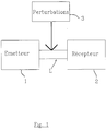
- Figure 1 shows the block diagram of a communication system.
- Figure 2 shows protection and filtering devices associated with a communication receiver.
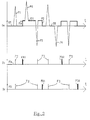
- Figure 3 shows the influence of disturbances on transmission lines and noise on the detection of signal transitions.
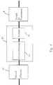
- Figure 4 shows the position of a digital filter according to the invention.
- FIG. 5 represents the initial signals, disturbed, then filtered according to an embodiment of the invention.
- FIG. 6 represents transmission signals, operating in synchronous mode, and filtered according to an embodiment of the invention.
- the block diagram in FIG. 1 represents a communication system between a transmitter 1 and a receiver 2 located in a disturbed industrial environment.
- the transmitter can be included in a circuit breaker, either inside an associated electronic trip unit, or in an auxiliary circuit, while the receiver can be part of the external and remote auxiliary circuits of the circuit breaker, such as signal boxes , remote control or network connection.
- a link L between the transmitter 1 and the receiver 2 can therefore be in an environment where the electromagnetic disturbances 3 are strong. These disturbances have generally a very short rise and fall time, which gives them a very high frequency spectrum.
- the link L receives, by electromagnetic induction or by capacitive coupling, energy in the form of parasitic transient currents or voltages, which are added to the signals normally transmitted by the link.
- the input circuits of a receiver 2 such as that of FIG. 2, have protection circuits 5 which clip the signals when their voltage exceeds positive or negative limit values.
- an analog filter 6 eliminates a large part of the noise without disturbing the useful signal.
- the filter consists of low-pass type cells made with resistors and capacitors or with inductors and resistors, but the efficiency of this type of filter is not always sufficient for high reliability of the transmission.
- the differentiation between a low state and a high state of a signal is carried out by a comparison circuit CO.
- the circuit 5, the filter 6 and the comparison circuit CO constitute an input circuit 13 of the receiver 2.
- the output signals from the comparison circuit are then directed to a processing circuit 4 intended for managing the communication.
- the processing circuit 4 is in a known manner, built around a microprocessor.
- the comparison circuit CO and the processing circuit 4 can be produced in the same integrated circuit and have a common supply Va, O.
- the processing circuit can detect the states of the logic signals, and / or the signal transitions between these states. The detection of transitions, rising edges or falling edges, is very sensitive to parasites.
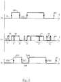
- FIG. 3 shows the detection of edges of a digital signal disturbed by parasites.
- the signal SP (curve 3a) loaded with parasites can take high states EH and low states EB between which must be detected rising edges FM and falling edges FD.
- the parasite sign being random, it can cause erroneous detection of rising edges (curve 3b) and / or falling edges (curve 3c).
- a positive parasite P1 appearing on a low state or a negative parasite P3 appearing on a high state generate the detection of rising Fp edges (curve 3b) and falling edges (curve 3c).
- a positive parasite P2 on a high state or a negative parasite P4 on a low state do not generate edge detection.
- parasitic fronts Fp are mixed with the real fronts FM1, FM2, FD1 and FD2 (curves 3b and 3c).
- a digital filter 14 is interposed between the input circuit 13 and the processing circuit 4.
- the digital filter 14 samples, or reads at regular intervals, and stores in memory a sampling circuit 15, the output signals from circuit 13, representative of the disturbed state of the signals transmitted on line L.
- the sampling frequency must be higher than the bit rate of the transmitted information and lower than the inverse of the duration of a parasite.
- These samples are analyzed in an analysis circuit 16 which outputs, after filtering, to the processing circuit 4, logic signals representative of the state of the signals transmitted on the line L, after elimination of the parasites.
- a logic state is considered to be true, by circuit 16, when a certain proportion of samples corresponding to this state is reached. This proportion is calculated at each sampling period for an analysis period comprising a predetermined number of successive samples.
- the detection of a high or low state is validated if at least 4 samples out of 8 successive samples are in the high state, or respectively low. Edge detection can be done on a lower number of samples. For example, if the processing circuit 4 must detect edges, the circuit 16 can use only 4 successive samples to detect a state, this being considered to be true if at least 3 samples out of 4 are in this state.
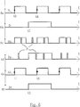
- a disturbed signal can be of the form represented in Sp (curve 5b).
- Sp curve 5b
- 3 samples out of 4 are in the low state and the filter 14 outputs a low state.
- the P5 parasite therefore does not alter the result.
- 3 samples out of 4 are in the high state and the falling edge of the parasite P6 is not detected.
- the transition to the low state and during the analysis period 10 the transition to the high state are detected.
- the analysis periods 7 to 10 correspond to 4 samples, the states thus detected being applied to the input of the processing circuit 4 for detection of the edges.
- the analysis periods 11 and 12 each include 8 samples to allow detection of the states by the processing circuit 4. During the analysis period 11, 7 samples out of 8 are in the high state, which eliminates the parasite P7 . The two parasites P8 do not modify the detection of the low state during the analysis period 12. The rising edges FMf1 and FMf2 and the falling edges FDf1 and FDf2 as well as the filtered high EHf and low EBf states (curve 5c) no longer has any parasites.
- FIG. 6 shows an application of the invention to a serial transmission system of the synchronous type.
- two signals are transmitted, namely a data signal D (curve 6b) and a clock signal H (curve 6a) intended to validate the state of the data on its rising edges.
- the rising edge of the clock must validate a low state at time to, while at time t4, it must validate a high state of the data signal.
- Disturbed signals from the clock Hp (curve 6c) and from data Dp (curve 6d) present parasites P which would cause erroneous additional data to be validated in the absence of any particular measurement.
- Digital filtering of the same type as in FIG.
- the functions of the comparison circuits CO, sampling 15, analysis 16 and processing 4 can be performed by means of a common microprocessor.
- the digital filter described above is particularly suitable for connections between transmitter and receiver in disturbed environments. It can be applied to serial links as well as to parallel links.
- the embodiments which have been described take account of two logic states (high and low), but the invention can be applied to signals comprising several distinct logic states. For example, for a signal which has 4 logic states represented by four voltage levels, a state can be detected when at least four out of eight samples correspond to this state. Reading of states or edges can be carried out simultaneously or sequentially, with a variable number of successive samples and a variable minimum number of samples.
- the digital filter can be integrated into the microprocessor of the processing circuit responsible for managing the transmission line in the receiver, but it can take other forms, in particular a filtering circuit independent of the main microprocessor of the receiver.
Landscapes
- Engineering & Computer Science (AREA)
- Power Engineering (AREA)
- Computer Networks & Wireless Communication (AREA)
- Signal Processing (AREA)
- Dc Digital Transmission (AREA)
- Arrangements For Transmission Of Measured Signals (AREA)
Applications Claiming Priority (2)
| Application Number | Priority Date | Filing Date | Title |
|---|---|---|---|
| FR9205846 | 1992-05-12 | ||
| FR9205846A FR2691311A1 (fr) | 1992-05-12 | 1992-05-12 | Dispositif de réception de signaux numériques comportant des moyens de filtrage. |
Publications (1)
| Publication Number | Publication Date |
|---|---|
| EP0574329A1 true EP0574329A1 (de) | 1993-12-15 |
Family
ID=9429776
Family Applications (1)
| Application Number | Title | Priority Date | Filing Date |
|---|---|---|---|
| EP93420169A Ceased EP0574329A1 (de) | 1992-05-12 | 1993-04-26 | Empfänger der Überabtastung zur Beseitigung von Störimpulsen verwendet |
Country Status (3)
| Country | Link |
|---|---|
| US (1) | US5663987A (de) |
| EP (1) | EP0574329A1 (de) |
| FR (1) | FR2691311A1 (de) |
Families Citing this family (2)
| Publication number | Priority date | Publication date | Assignee | Title |
|---|---|---|---|---|
| FR2738701A1 (fr) * | 1995-09-13 | 1997-03-14 | Trt Telecom Radio Electr | Systeme de transmission a sensibilite au bruit diminuee |
| DE19823705A1 (de) * | 1998-05-27 | 1999-12-02 | Siemens Ag | Verfahren und Schaltungsanordung zum Wiederherstellen eines Binärsignals |
Citations (5)
| Publication number | Priority date | Publication date | Assignee | Title |
|---|---|---|---|---|
| US3480910A (en) * | 1963-11-04 | 1969-11-25 | Ibm | Pulse value determining receiver |
| US3938081A (en) * | 1973-05-03 | 1976-02-10 | Kirk Robert T | Circuitry for preventing the use of erroneous data |
| US4317111A (en) * | 1978-04-11 | 1982-02-23 | Ing. C. Olivetti & C., S.P.A. | Digital device for synchronizing and decoding coded signals |
| EP0051141A1 (de) * | 1980-11-04 | 1982-05-12 | LGZ LANDIS & GYR ZUG AG | Verfahren und Einrichtung zur Entzerrung binärer Empfangssignale |
| US4358846A (en) * | 1979-07-27 | 1982-11-09 | The United States Of America As Represented By The Administrator Of The National Aeronautics And Space Administration | Serial data correlator/code translator |
Family Cites Families (2)
| Publication number | Priority date | Publication date | Assignee | Title |
|---|---|---|---|---|
| US5001374A (en) * | 1989-09-08 | 1991-03-19 | Amp Incorporated | Digital filter for removing short duration noise |
| CN1062963C (zh) * | 1990-04-12 | 2001-03-07 | 多尔拜实验特许公司 | 用于产生高质量声音信号的解码器和编码器 |
-
1992
- 1992-05-12 FR FR9205846A patent/FR2691311A1/fr not_active Withdrawn
-
1993
- 1993-04-26 EP EP93420169A patent/EP0574329A1/de not_active Ceased
- 1993-05-06 US US08/057,785 patent/US5663987A/en not_active Expired - Fee Related
Patent Citations (5)
| Publication number | Priority date | Publication date | Assignee | Title |
|---|---|---|---|---|
| US3480910A (en) * | 1963-11-04 | 1969-11-25 | Ibm | Pulse value determining receiver |
| US3938081A (en) * | 1973-05-03 | 1976-02-10 | Kirk Robert T | Circuitry for preventing the use of erroneous data |
| US4317111A (en) * | 1978-04-11 | 1982-02-23 | Ing. C. Olivetti & C., S.P.A. | Digital device for synchronizing and decoding coded signals |
| US4358846A (en) * | 1979-07-27 | 1982-11-09 | The United States Of America As Represented By The Administrator Of The National Aeronautics And Space Administration | Serial data correlator/code translator |
| EP0051141A1 (de) * | 1980-11-04 | 1982-05-12 | LGZ LANDIS & GYR ZUG AG | Verfahren und Einrichtung zur Entzerrung binärer Empfangssignale |
Also Published As
| Publication number | Publication date |
|---|---|
| US5663987A (en) | 1997-09-02 |
| FR2691311A1 (fr) | 1993-11-19 |
Similar Documents
| Publication | Publication Date | Title |
|---|---|---|
| EP0062572B1 (de) | Kapazitives Tastenfeld mit gegen Störungen wirksamer Struktur | |
| BE898477A (fr) | Système de transmission de signaux digitaux. | |
| EP0125723A1 (de) | Vom Basisband ausgehend gesteuerte Trägerfrequenzentzerrereinrichtung | |
| EP0427638A1 (de) | Leitungschnittstelle für ein Nachrichtenübertragungsnetz | |
| EP2726888B1 (de) | Verfahren und vorrichtung zur steuerung einer gasisolierten elektrischen hochspannungsschaltanlage | |
| EP0369833A1 (de) | Zugriffseinheit für einen Übertragungsweg eines lokalen Netzes | |
| FR2525006A1 (fr) | Detecteur d'intrusion | |
| EP0014505A1 (de) | System zum Prüfen einer mit einem Echo-Unterdrücker ausgerüsteten Vorrichtung | |
| EP0058095B1 (de) | Gerät zur Bestimmung der Ankunftszeit von Impulsen mit DME-Verwendungszweck | |
| EP0359633B1 (de) | Logarithmischer Hüllkurvendetektor für ein analoges Signal | |
| WO1980001516A1 (fr) | Perfectionnement aux transformateurs capacitifs de tension | |
| EP0574329A1 (de) | Empfänger der Überabtastung zur Beseitigung von Störimpulsen verwendet | |
| EP0966800B1 (de) | Steuervorrichtung für trägerstromübertragung auf einem niedervoltnetz | |
| US20050135468A1 (en) | Feed forward filter | |
| WO2019106249A1 (fr) | Système à boucle de masse intégrant un dispositif de couplage électrique agissant sur un courant parasite | |
| FR2623670A1 (fr) | Circuit analogique pour modem en bande de base | |
| EP0905946A1 (de) | Reglung der Abtastung von Biphasensignale | |
| EP1612985B1 (de) | Zweiwegsvermittlung | |
| US20050135473A1 (en) | Filter with signal taps temporally spaced at fractional symbol intervals | |
| FR2674392A1 (fr) | Systeme de transmission de signaux auxiliaires sur une liaison optique. | |
| EP0365401B1 (de) | Vergleichsschaltung mit variabler Hysterese für eine digitale Audio-Empfangsschnittstelle | |
| EP0494555B1 (de) | Leitungsempfänger für ein Nachrichtenübertragungsnetz | |
| EP0404001B1 (de) | Signalisierungsdetektor für Gebührensignalisierung für eine Telefonverbindungsleitung | |
| EP3258682B1 (de) | Analoge signalverarbeitunskette | |
| CA2324430A1 (fr) | Dispositif et boitier pour raccordement a un reseau local |
Legal Events
| Date | Code | Title | Description |
|---|---|---|---|
| PUAI | Public reference made under article 153(3) epc to a published international application that has entered the european phase |
Free format text: ORIGINAL CODE: 0009012 |
|
| AK | Designated contracting states |
Kind code of ref document: A1 Designated state(s): DE ES GB IT |
|
| 17P | Request for examination filed |
Effective date: 19940516 |
|
| RAP1 | Party data changed (applicant data changed or rights of an application transferred) |
Owner name: SCHNEIDER ELECTRIC SA |
|
| 17Q | First examination report despatched |
Effective date: 19961125 |
|
| GRAG | Despatch of communication of intention to grant |
Free format text: ORIGINAL CODE: EPIDOS AGRA |
|
| RAP1 | Party data changed (applicant data changed or rights of an application transferred) |
Owner name: SCHNEIDER ELECTRIC INDUSTRIES SA |
|
| STAA | Information on the status of an ep patent application or granted ep patent |
Free format text: STATUS: THE APPLICATION HAS BEEN REFUSED |
|
| 18R | Application refused |
Effective date: 20000228 |