EP0574672A1 - Générateur ajustable de configurations aléatoires pondérées de test pour des circuits logiques - Google Patents
Générateur ajustable de configurations aléatoires pondérées de test pour des circuits logiques Download PDFInfo
- Publication number
- EP0574672A1 EP0574672A1 EP93106489A EP93106489A EP0574672A1 EP 0574672 A1 EP0574672 A1 EP 0574672A1 EP 93106489 A EP93106489 A EP 93106489A EP 93106489 A EP93106489 A EP 93106489A EP 0574672 A1 EP0574672 A1 EP 0574672A1
- Authority
- EP
- European Patent Office
- Prior art keywords
- output
- logic circuit
- probability
- latch
- pattern generator
- Prior art date
- Legal status (The legal status is an assumption and is not a legal conclusion. Google has not performed a legal analysis and makes no representation as to the accuracy of the status listed.)
- Withdrawn
Links
Images



Classifications
-
- G—PHYSICS
- G01—MEASURING; TESTING
- G01R—MEASURING ELECTRIC VARIABLES; MEASURING MAGNETIC VARIABLES
- G01R31/00—Arrangements for testing electric properties; Arrangements for locating electric faults; Arrangements for electrical testing characterised by what is being tested not provided for elsewhere
- G01R31/28—Testing of electronic circuits, e.g. by signal tracer
- G01R31/317—Testing of digital circuits
- G01R31/3181—Functional testing
- G01R31/31813—Test pattern generators
-
- G—PHYSICS
- G01—MEASURING; TESTING
- G01R—MEASURING ELECTRIC VARIABLES; MEASURING MAGNETIC VARIABLES
- G01R31/00—Arrangements for testing electric properties; Arrangements for locating electric faults; Arrangements for electrical testing characterised by what is being tested not provided for elsewhere
- G01R31/28—Testing of electronic circuits, e.g. by signal tracer
- G01R31/317—Testing of digital circuits
- G01R31/3181—Functional testing
- G01R31/3183—Generation of test inputs, e.g. test vectors, patterns or sequences
- G01R31/318385—Random or pseudo-random test pattern
-
- G—PHYSICS
- G06—COMPUTING OR CALCULATING; COUNTING
- G06F—ELECTRIC DIGITAL DATA PROCESSING
- G06F7/00—Methods or arrangements for processing data by operating upon the order or content of the data handled
- G06F7/58—Random or pseudo-random number generators
- G06F7/582—Pseudo-random number generators
- G06F7/584—Pseudo-random number generators using finite field arithmetic, e.g. using a linear feedback shift register
-
- G—PHYSICS
- G06—COMPUTING OR CALCULATING; COUNTING
- G06F—ELECTRIC DIGITAL DATA PROCESSING
- G06F2207/00—Indexing scheme relating to methods or arrangements for processing data by operating upon the order or content of the data handled
- G06F2207/58—Indexing scheme relating to groups G06F7/58 - G06F7/588
- G06F2207/581—Generating an LFSR sequence, e.g. an m-sequence; sequence may be generated without LFSR, e.g. using Galois Field arithmetic
-
- G—PHYSICS
- G06—COMPUTING OR CALCULATING; COUNTING
- G06F—ELECTRIC DIGITAL DATA PROCESSING
- G06F2207/00—Indexing scheme relating to methods or arrangements for processing data by operating upon the order or content of the data handled
- G06F2207/58—Indexing scheme relating to groups G06F7/58 - G06F7/588
- G06F2207/583—Serial finite field implementation, i.e. serial implementation of finite field arithmetic, generating one new bit or trit per step, e.g. using an LFSR or several independent LFSRs; also includes PRNGs with parallel operation between LFSR and outputs
Definitions
- the invention relates to test pattern generators for logic circuits.
- Logic circuits for data processing and other apparatus typically consist of a network of interconnected logic gates, such as “AND” gates, “OR” gates, “NAND” gates, “NOR” gates, “NOT” gates, “XOR” gates, and so on.
- the network of gates has a number of inputs for receiving digits, and has a number of outputs for outputting digits.
- the logic circuit is designed such that for each input digit pattern, of a set of one or more input digit patterns, provided at the inputs of the network, a corresponding predetermined output digit pattern is produced at the outputs of the network.
- the observed output digit patterns produced at the outputs of the network will differ from the expected predetermined output digit patterns.
- One way to test for faults in a logic circuit is to apply each possible input digit pattern at the inputs of the logic network, and to compare the actual output digit pattern with the expected output digit pattern. For small numbers of possible input digit patterns, the cost of storing the input digit patterns and performing this deterministic testing is reasonable. However, for large numbers of possible input digit patterns, the cost of such deterministic testing is too high.
- An alternative method of testing for faults in a logic circuit is to apply random input digit test patterns at the inputs of the logic network, and to compare the actual output digit patterns with the expected output digit patterns.
- the number of random test patterns needed to achieve a selected level of confidence that a logic circuit contains no faults depends on the set of input digit patterns for which the logic circuit is designed.
- Another alternative method of testing for faults in a logic circuit is to apply one or more weighted random input digit test patterns at the inputs of a logic network, and to compare the actual output digit patterns with the expected output digit patterns.
- a weighted random input digit test pattern there is at least one digit for which the probability of occurence of one value is different from 1/N, where N is the number of different possible values of the digit.
- the weights W may be uniform across all digits in the test pattern, or the weights may be nonuniform.
- the weighted random test patterns are selected to achieve, efficiently and at low cost, a desired level of confidence that the logic circuit contains no faults. Weighted random testing can significantly decrease the number of test patterns which must be applied to a logic circuit to obtain the same test effectiveness as an unweighted random test.
- test pattern generator for selectively generating multiple different weighted random test patterns, and particularly multiple different nonuniform weighted random test patterns.
- an apparatus for generating test patterns comprises a random pattern generator for generating a series of digit signals at an output of the random pattern generator.
- Each digit signal in the series has an initial probability of having a first value. The initial probability is adjustable.
- a shift register for storing a plurality of digit signals of a test pattern.
- the shift register has an input for receiving digit signals from the output of the random pattern generator.
- the shift register has a plurality of outputs for outputting a test pattern comprising the stored digit signals.
- the shift register comprises a series of latches and at least a first logic circuit.
- Each latch in the series of latches has an input and has an output.
- the input of a first latch is connected to the output of the random pattern generator.
- the output of each latch is connected to the input of a next adjacent latch.
- Each latch stores one digit signal of a test pattern.
- the first logic circuit connects the output of the random pattern generator to the input of the first latch or connects the output of a latch to the input of a next adjacent latch.
- the logic circuit has first and second states, and a control input for selecting either the first state or the second state.
- the logic circuit has a data output for outputting a series of digit signals. Each digit signal output by the logic circuit has a first output probability of having the first value when the logic circuit is in the first state. The first output probability is independent of the initial probability produced by the random pattern generator. Each digit signal output by the logic circuit has a second output probability of having the first value when the logic circuit is in the second state. The second output probability is dependent upon the initial probability produced by the random pattern generator.
- the latch may be, for example, a binary electronic latch in which each digit signal has one of only first and second values.
- the first value of the digit signal may, for example, represent one.
- the second value of the digit signal may, for example, represent zero.
- the logic circuit may comprise, for example, a logical OR gate having a first input connected to the output of the random pattern generator or to the output of a latch.
- the logical OR gate has a second input connected to a control line.
- the logic circuit may comprise a logical AND gate having a first input connected to the output of the random pattern generator, or to the output of a latch.
- the logical AND gate has a second input connected to a control line.
- each latch has an input for receiving digit signals from the output of the logic circuit or from the output of a prior adjacent latch.
- Each latch has an output for outputting digit signals to a circuit to be tested.
- the apparatus for generating test patterns may further comprise a second logic circuit for connecting the output of a latch to the input of a next adjacent latch.
- the first logic circuit is arranged in the shift register between the random pattern generator and the second logic circuit.
- test pattern generator having at least one logic circuit having a first state in which the output probability of the logic circuit is independent of the output probability of the random pattern generator, and having a second state in which the output probability of the logic circuit is dependent on the output probability of the random pattern generator, it is possible to generate two or more different uniform or nonuniform weighted random test patterns.
- the test pattern generator can be provided within a small area of an electronic chip containing the logic circuit to be tested, and the generator will not interfere with the operation of the logic circuit to be tested.
- test pattern generator for selectively generating multiple different weighted random test patterns, which test pattern generator can be provided within a small area of an electronic chip containing a logic circuit to be tested.
- test pattern generator for selectively generating multiple different weighted random test, which test pattern generator does not interfere with or impact the performance of the logic circuit to be tested.
- Figure 1 is a block diagram of an example of an apparatus for generating test patterns according to the present invention.
- the apparatus comprises a random pattern generator 10 for generating a series of digit signals at an output of the random pattern generator.
- Each digit signal in the series has an initial probability of having a first value.
- the initial probability is adjustable.
- each digit signal has one of only first and second values.
- the first value of the digit signal may, for example, represent one.
- the second value of the digit signal may, for example, represent zero.
- the probabilities P 1 and P 0 are adjustable.
- the apparatus for generating test patterns further comprises a shift register 12.
- the shift register 12 stores a plurality of digit signals of a test pattern.
- the shift register 12 has an input 14 for receiving digit signals from the output of the random pattern generator 10.
- the shift register 12 has a plurality of outputs 16 for outputting a test pattern comprising the stored digit signals.
- the test pattern output from shift register 12 is provided to the input of a logic circuit 18 to be tested.
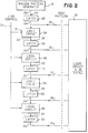
- FIG. 2 shows a more detailed block diagram of an example of an apparatus for generating test patterns according to the present invention.
- the shift register 12 comprises a series of latches 20. While five latches are shown, the number of latches will depend on the desired number of digits in the test pattern.
- Each latch 20 has an input 22 and has an output 24. The input of a first latch 20 is connected to an output 26 of the random pattern generator 10. The output 24 of each latch 20 is connected to the input 22 of a next adjacent latch.
- Each latch 20 stores one digit signal of a test pattern.
- the shift register 12 further comprises at least a first logic circuit 28 for connecting the output 26 of the random generator 10 to the input 22 of the first latch 20 (as shown in Figure 2).
- shift register 12 comprises a logic circuit 36 for connecting the output 24 of one latch 20 to the input 22 of a next adjacent latch 20.
- Logic circuit 28 has first and second states, and a control input 30 for selecting either the first or the second state.
- the logic circuit 28 has a data output 32 for out-putting a series of digit signals.
- Each digit signal output by the logic circuit 28 has a first output probability of having the first value when the logic circuit is in the first state.
- the first output probability from logic circuit 28 is independent of the initial probability produced by random pattern generator 10.
- Each digit signal output by the logic circuit 28 has a second output probability of having the first value when the logic circuit is in the second state.
- the second output probability of logic circuit 28 is dependent upon the initial probability produced by random pattern generator 10.
- a control line 34 is connected to the control input 30 of logic circuit 28 for selecting either the first or the second state of logic circuit 28.
- the apparatus for generating test patterns according to the invention may further comprise one or more second logic circuits 36.
- Each second logic circuit 36 connects the output 24 of a latch 20 to the input 22 of a next adjacent latch 20.
- the first logic circuit 28 is arranged in the shift register 12 between the random pattern generator 10 and second logic circuits 36.
- Each latch 20 in the apparatus for generating test patterns is preferably a binary electronic latch such as a flip-flop circuit.
- Each logic circuit 28 or 36 may, for example, have more than two states.
- Logic circuits 28 and 36 having three or four states can be provided with two binary control inputs 38 connected to two control lines 40 and 42 as shown in Figure 3, in order to select one of the four states of the logic circuit.
- Figure 4 is a more detailed block diagram of another example of an apparatus for generating test patterns according to the present invention.
- logic circuit A When logic circuit A is in State 1, the probability that logic circuit A will output a 1 is P, and the probability of outputting 0 is 1-P, where the probability that random pattern generator 10 will output a 1 is P. In State 1, the output probabilities of logic circuit A are dependent on the initial output probability P produced by the random pattern generator 10.
- the apparatus of Figure 4 comprises a NOT gate 50 whose output is the inverse of its input.
- NOT gate 50 has no control input.
- the apparatus shown in Figure 4 also includes a logic circuit formed by XOR gate 52 (an exclusive OR gate) and NOT gate 54.
- NOT gate 54 has a control input connected to the control line 34.
- the output of XOR gate 52 will be equal to its input when control line 34 has a value of 1.
- the output of XOR gate 52 will be the inverse of its input when control line 34 has a value of 0. Consequently, in both states of this logic circuit, the output probabilities are dependent on the initial output probability P of random pattern generator 10.
- Table 3 shows an example of how to operate the test pattern generator shown in Figure 4.
- random pattern generator 10 For each time interval, random pattern generator 10 generates a digit signal having a probability P of representing 1. For each time interval, the digit signal generated by random pattern generator 10 is shifted into the first adjacent latch 20. For each time interval, the digit signal stored in each latch 20 is shifted to the next adjacent latch 20.
- a first nonuniform weighted random test pattern can be selected by applying a value of 0 to control line 34.
- a second nonuniform weighted random test pattern can be obtained by applying a value of 1 to control line 34.
- Figure 5 shows another example of an apparatus for generating test patterns according to the invention.
- the latches and gates of Figure 5 correspond to those of Figure 4, except for logic circuit C of Figure 5.
- Logic circuit C comprises OR gate 56, AND gate 58, and NOT gate 60.
- OR gate 56 has a control input connected to control line 40.
- NOT gate 60 has a control input connected to control line 42.
- logic circuit 3 is in State 1 when control line 40 has a value of 0, and control line 42 has a value of 0.
- Logic circuit C is in State 2 when control line 40 has a value of 1, and control line 42 has a value of 0.
- Logic circuit C in State 3 when control line 40 has a value of 1, and control line 42 has a value of 1.
- logic circuit C when logic circuit C is in State 2 or State 3, the output probabilities of logic circuit C are independent of the initial output probability of random pattern generator 10. In State 2, the probability that logic circuit C will output a 1 is one, and the probability that logic circuit C will output 0 is zero. In State 3, the probability that logic circuit C will output a 1 is zero, and the probability that logic circuit C will output 0 is one.
- Table 5 shows one method of using the test pattern generator of Figure 5 in order to generate weighted random patterns.
- both control line 40 and control line 42 have values of 0.
- the values of control lines 40 and 42 may be selected as shown in Table 5 to choose one of three possible nonuniform weighted random test patterns.
- Figure 6 is a block diagram of an example of a random pattern generator 10.
- the random pattern generator comprises a linear feedback shift register having a series of latches 62 separated by XOR gates 64. There may be, for example, thirty-two latches 62 forming a thirty-two bit linear feedback shift register.
- a multiplexer 66 has weight select inputs for selecting one of four inputs for connection to its output.
- the first input is the last bit of the linear feedback shift register, and has a probability of 1 2 of generating a 1.
- the second input to multiplexer 66 is the output of AND gate 68, which performs an AND function on the last two bits of the linear feedback shift register.
- the output of AND gate 68 has a probability of 1 4 of generating a 1.
- the third input to multiplexer 66 is the output of AND gate 70, which performs an AND function on the last three bits of the linear feedback shift register.
- the output of AND gate 70 has a probability of 1 8 of generating a 1.
- the fourth input to multiplexer 66 is AND gate 72 which performs an AND function on the last four bits of the linear feedback shift register.
- the output of AND gate 72 has a probability of 1 16 of generating a 1.
- the output of multiplexer 66 is provided to one input of XOR gate 74.
- Another input of XOR gate 74 selects a weighted value of "O" or "1" for the output probabilities of 1 2 , 1 4 , 1 8 , and 1 16 ,
Landscapes
- Physics & Mathematics (AREA)
- General Physics & Mathematics (AREA)
- Engineering & Computer Science (AREA)
- General Engineering & Computer Science (AREA)
- Theoretical Computer Science (AREA)
- Computational Mathematics (AREA)
- Mathematical Analysis (AREA)
- Mathematical Optimization (AREA)
- Pure & Applied Mathematics (AREA)
- Tests Of Electronic Circuits (AREA)
- Test And Diagnosis Of Digital Computers (AREA)
Applications Claiming Priority (2)
| Application Number | Priority Date | Filing Date | Title |
|---|---|---|---|
| US07/900,706 US5297151A (en) | 1992-06-17 | 1992-06-17 | Adjustable weighted random test pattern generator for logic circuits |
| US900706 | 1992-06-17 |
Publications (1)
| Publication Number | Publication Date |
|---|---|
| EP0574672A1 true EP0574672A1 (fr) | 1993-12-22 |
Family
ID=25412964
Family Applications (1)
| Application Number | Title | Priority Date | Filing Date |
|---|---|---|---|
| EP93106489A Withdrawn EP0574672A1 (fr) | 1992-06-17 | 1993-04-21 | Générateur ajustable de configurations aléatoires pondérées de test pour des circuits logiques |
Country Status (3)
| Country | Link |
|---|---|
| US (1) | US5297151A (fr) |
| EP (1) | EP0574672A1 (fr) |
| JP (1) | JP2823475B2 (fr) |
Families Citing this family (16)
| Publication number | Priority date | Publication date | Assignee | Title |
|---|---|---|---|---|
| JP2584172B2 (ja) * | 1991-08-23 | 1997-02-19 | インターナショナル・ビジネス・マシーンズ・コーポレイション | デイジタル試験信号発生回路 |
| JPH05119122A (ja) * | 1991-10-25 | 1993-05-18 | Fujitsu Ltd | スキヤン回路のテストパターン生成方法 |
| US5596587A (en) * | 1993-03-29 | 1997-01-21 | Teradyne, Inc. | Method and apparatus for preparing in-circuit test vectors |
| JP3202439B2 (ja) * | 1993-10-07 | 2001-08-27 | 富士通株式会社 | 出力装置のテスト装置 |
| US5642362A (en) * | 1994-07-20 | 1997-06-24 | International Business Machines Corporation | Scan-based delay tests having enhanced test vector pattern generation |
| US5682392A (en) * | 1994-09-28 | 1997-10-28 | Teradyne, Inc. | Method and apparatus for the automatic generation of boundary scan description language files |
| US5684946A (en) * | 1995-09-11 | 1997-11-04 | Digital Equipment Corporation | Apparatus and method for improving the efficiency and quality of functional verification |
| US5983380A (en) * | 1997-09-16 | 1999-11-09 | International Business Machines Corporation | Weighted random pattern built-in self-test |
| US6173424B1 (en) | 1997-12-31 | 2001-01-09 | Micron Technology, Inc. | Programmable pulse generator and method for using same |
| US6662327B1 (en) | 1998-05-13 | 2003-12-09 | Janusz Rajski | Method for clustered test pattern generation |
| US6314540B1 (en) | 1999-04-12 | 2001-11-06 | International Business Machines Corporation | Partitioned pseudo-random logic test for improved manufacturability of semiconductor chips |
| US6910165B2 (en) | 2001-02-28 | 2005-06-21 | International Business Machines Corporation | Digital random noise generator |
| US6983407B2 (en) * | 2002-06-14 | 2006-01-03 | International Business Machines Corporation | Random pattern weight control by pseudo random bit pattern generator initialization |
| US6880136B2 (en) * | 2002-07-09 | 2005-04-12 | International Business Machines Corporation | Method to detect systematic defects in VLSI manufacturing |
| JP6721423B2 (ja) * | 2016-06-14 | 2020-07-15 | 株式会社日立製作所 | アプリロジックおよびその検証方法 |
| JP2018116545A (ja) * | 2017-01-19 | 2018-07-26 | オムロン株式会社 | 予測モデル作成装置、生産設備監視システム、及び生産設備監視方法 |
Citations (2)
| Publication number | Priority date | Publication date | Assignee | Title |
|---|---|---|---|---|
| DE3639577A1 (de) * | 1986-11-20 | 1988-05-26 | Siemens Ag | Logikbaustein zur erzeugung von ungleich verteilten zufallsmustern fuer integrierte schaltungen |
| WO1991003014A2 (fr) * | 1989-08-25 | 1991-03-07 | Mcnc | Procede et appareil de generation de configuration aleatoire ponderee de haute precision |
Family Cites Families (1)
| Publication number | Priority date | Publication date | Assignee | Title |
|---|---|---|---|---|
| US4817093A (en) * | 1987-06-18 | 1989-03-28 | International Business Machines Corporation | Method of partitioning, testing and diagnosing a VLSI multichip package and associated structure |
-
1992
- 1992-06-17 US US07/900,706 patent/US5297151A/en not_active Expired - Fee Related
-
1993
- 1993-04-20 JP JP5093124A patent/JP2823475B2/ja not_active Expired - Lifetime
- 1993-04-21 EP EP93106489A patent/EP0574672A1/fr not_active Withdrawn
Patent Citations (2)
| Publication number | Priority date | Publication date | Assignee | Title |
|---|---|---|---|---|
| DE3639577A1 (de) * | 1986-11-20 | 1988-05-26 | Siemens Ag | Logikbaustein zur erzeugung von ungleich verteilten zufallsmustern fuer integrierte schaltungen |
| WO1991003014A2 (fr) * | 1989-08-25 | 1991-03-07 | Mcnc | Procede et appareil de generation de configuration aleatoire ponderee de haute precision |
Also Published As
| Publication number | Publication date |
|---|---|
| US5297151A (en) | 1994-03-22 |
| JPH0651028A (ja) | 1994-02-25 |
| JP2823475B2 (ja) | 1998-11-11 |
Similar Documents
| Publication | Publication Date | Title |
|---|---|---|
| EP0574672A1 (fr) | Générateur ajustable de configurations aléatoires pondérées de test pour des circuits logiques | |
| DE60116046T2 (de) | Eingebaute Selbsttestschaltung mit einem Schieberegister mit linearer Rückkopplung | |
| EP0541537B1 (fr) | Procede et appareil de generation de configuration aleatoire ponderee de haute precision | |
| US5644578A (en) | Failure memory device | |
| EP0529290B1 (fr) | Auto-test des circuits intégrés avec des configurations hybrides | |
| US5938784A (en) | Linear feedback shift register, multiple input signature register, and built-in self test circuit using such registers | |
| AU608439B2 (en) | Dynamic feedback arrangement scrambling technique keystream generator | |
| JP2598866B2 (ja) | 制御可能な重み付き2進シーケンスを発生するための回路 | |
| EP0372226A2 (fr) | Générateur de configurations pseudo-aléatoire parallèle à décalage variant de phase et méthode pour le simuler | |
| EP0632468A1 (fr) | Circuit de compression de données rapides pour puces de mémoire à semi-conducteurs avec auto-test incorporé | |
| KR0156152B1 (ko) | 최대값 선택회로 | |
| EP0088202A2 (fr) | Générateur de séquence d'adresses de mémoire | |
| EP0266873B1 (fr) | Réseau logique programmable | |
| US5835428A (en) | Method of testing semiconductor memory and apparatus for carrying out the method | |
| EP1435005B1 (fr) | Systeme numerique et procede de detection d'erreur correspondant | |
| US5703818A (en) | Test circuit | |
| US4418410A (en) | Error detection and correction apparatus for a logic array | |
| KR970005278B1 (ko) | 부분적으로 디코드된 테스트 어드레스 발생기 및 카운트 발생 방법 | |
| EP0266874B1 (fr) | Réseau logique programmable | |
| US7002493B2 (en) | Boolean logic tree reduction circuit | |
| US5038349A (en) | Method for reducing masking of errors when using a grid-based, "cross-check" test structure | |
| KR100206124B1 (ko) | 자기테스트회로 | |
| KR100227789B1 (ko) | 메모리 테스트 패턴 생성기 | |
| KR100444763B1 (ko) | 내장된 자체테스트 기법을 위한 결정패턴 생성기 | |
| EP0206468A1 (fr) | Tester des circuits intégrés digitaux |
Legal Events
| Date | Code | Title | Description |
|---|---|---|---|
| PUAI | Public reference made under article 153(3) epc to a published international application that has entered the european phase |
Free format text: ORIGINAL CODE: 0009012 |
|
| AK | Designated contracting states |
Kind code of ref document: A1 Designated state(s): DE FR GB |
|
| 17P | Request for examination filed |
Effective date: 19940429 |
|
| 18W | Application withdrawn |
Withdrawal date: 19940928 |