EP0574919A2 - Générateur de diagramme de transition d'état et générateur de configurations de test - Google Patents
Générateur de diagramme de transition d'état et générateur de configurations de test Download PDFInfo
- Publication number
- EP0574919A2 EP0574919A2 EP93109708A EP93109708A EP0574919A2 EP 0574919 A2 EP0574919 A2 EP 0574919A2 EP 93109708 A EP93109708 A EP 93109708A EP 93109708 A EP93109708 A EP 93109708A EP 0574919 A2 EP0574919 A2 EP 0574919A2
- Authority
- EP
- European Patent Office
- Prior art keywords
- state
- value
- fault
- input
- pseudo
- Prior art date
- Legal status (The legal status is an assumption and is not a legal conclusion. Google has not performed a legal analysis and makes no representation as to the accuracy of the status listed.)
- Withdrawn
Links
Images










Classifications
-
- G—PHYSICS
- G01—MEASURING; TESTING
- G01R—MEASURING ELECTRIC VARIABLES; MEASURING MAGNETIC VARIABLES
- G01R31/00—Arrangements for testing electric properties; Arrangements for locating electric faults; Arrangements for electrical testing characterised by what is being tested not provided for elsewhere
- G01R31/28—Testing of electronic circuits, e.g. by signal tracer
- G01R31/317—Testing of digital circuits
- G01R31/3181—Functional testing
- G01R31/3183—Generation of test inputs, e.g. test vectors, patterns or sequences
- G01R31/318342—Generation of test inputs, e.g. test vectors, patterns or sequences by preliminary fault modelling, e.g. analysis, simulation
- G01R31/318357—Simulation
-
- G—PHYSICS
- G01—MEASURING; TESTING
- G01R—MEASURING ELECTRIC VARIABLES; MEASURING MAGNETIC VARIABLES
- G01R31/00—Arrangements for testing electric properties; Arrangements for locating electric faults; Arrangements for electrical testing characterised by what is being tested not provided for elsewhere
- G01R31/28—Testing of electronic circuits, e.g. by signal tracer
- G01R31/317—Testing of digital circuits
- G01R31/3181—Functional testing
- G01R31/3183—Generation of test inputs, e.g. test vectors, patterns or sequences
- G01R31/318371—Methodologies therefor, e.g. algorithms, procedures
-
- G—PHYSICS
- G01—MEASURING; TESTING
- G01R—MEASURING ELECTRIC VARIABLES; MEASURING MAGNETIC VARIABLES
- G01R31/00—Arrangements for testing electric properties; Arrangements for locating electric faults; Arrangements for electrical testing characterised by what is being tested not provided for elsewhere
- G01R31/28—Testing of electronic circuits, e.g. by signal tracer
- G01R31/317—Testing of digital circuits
- G01R31/3181—Functional testing
- G01R31/3183—Generation of test inputs, e.g. test vectors, patterns or sequences
- G01R31/318392—Generation of test inputs, e.g. test vectors, patterns or sequences for sequential circuits
-
- G—PHYSICS
- G06—COMPUTING OR CALCULATING; COUNTING
- G06F—ELECTRIC DIGITAL DATA PROCESSING
- G06F30/00—Computer-aided design [CAD]
- G06F30/30—Circuit design
- G06F30/32—Circuit design at the digital level
- G06F30/33—Design verification, e.g. functional simulation or model checking
- G06F30/3323—Design verification, e.g. functional simulation or model checking using formal methods, e.g. equivalence checking or property checking
-
- G—PHYSICS
- G01—MEASURING; TESTING
- G01R—MEASURING ELECTRIC VARIABLES; MEASURING MAGNETIC VARIABLES
- G01R31/00—Arrangements for testing electric properties; Arrangements for locating electric faults; Arrangements for electrical testing characterised by what is being tested not provided for elsewhere
- G01R31/28—Testing of electronic circuits, e.g. by signal tracer
- G01R31/317—Testing of digital circuits
- G01R31/3181—Functional testing
- G01R31/3183—Generation of test inputs, e.g. test vectors, patterns or sequences
- G01R31/318342—Generation of test inputs, e.g. test vectors, patterns or sequences by preliminary fault modelling, e.g. analysis, simulation
Definitions
- the present invention relates to a state transition graph generator for a synchronous sequential circuit and also to a test pattern generator using such a graph generator.
- a known state transition graph generator is described, for example, in "Implicited State Enumeration of Finite State Machines using BDD's," Proc. ICCAD-90, pp. 130-133, Nov. 1990.
- a logic circuit is expressed in terms of a tree structure called a binary decision graph (BDD) and applied to the generation of a state transition graph.
- BDD binary decision graph
- Fig.1 shows the structure of this known state transition graph generator.
- This generator comprises a binary decision graph (BDD) simulator 2301 which expresses a sequential circuit in terms of a BDD and finds an aggregate of states x(t + 1) to which a transition can be made from a state x(t) at time t as well as an input value necessary for the transition, the aggregate of the states appearing at the next time (t + 1).
- a state aggregate-managing portion 2302 is a means for managing the aggregate of all states ⁇ x i (t)
- i 1, ..., N(t) ⁇ (where N(t) is the number of states reached at the time t) which are reached from the initial state up to the time t.
- a state search portion 2303 drives the BDD simulator, using the state aggregate in the state transition-managing portion 2302 at the time t.
- Signal lines 2310-2312 interconnect the various blocks.
- the BDD simulator 2310 expresses a logic circuit in terms of a BDD.
- Fig.2 shows an example in which a simple logic circuit is expressed in terms of a BDD.
- a node 241 indicates that a signal line A takes logic 1.
- a node 242 indicates that a signal line B takes logic 1.
- a block 243 indicates that the logic value of a signal line Z takes logic 1.
- These nodes indicate that the signal Z takes logic 1, provided that both signal lines A and B take logic 1.
- the BDD gives a graphic representation of a true value table, and it is relatively easy to understand how input values are assigned to obtain a given output value.
- the state search portion 2303 selects one from an aggregate of all states ⁇ x i (t)
- i 1, ..., N(t) ⁇ reached at time t (where N(t) is the number of states reached at time t) and outputs the selected ones to the signal line 2312.
- the BDD simulator 2301 finds the subsequent state (state appearing at the next time) which can be reached from that state, as well as input values leading to each state, and outputs these states to the signal line 2310.
- the state aggregate-managing portion 2302 stores input values corresponding to the aforementioned subsequent states output to the signal line 2310. The processing described above is repeated N(t) times.
- the state aggregate-managing portion 2302 finds the aggregate of said subsequent states ⁇ x i (t+1)
- i 1, ..., N(t+1) ⁇ and outputs this aggregate to the signal line 2311.
- N(t+1) N(t), i.e., a transition to a new state is not discovered, then the search is terminated. If N(t+1) > N(t), i.e., a transition to a new state is discovered, then the time is advanced to the next time, and control goes to step 2.
- the prior art state transition graph generator expresses a logic circuit in terms of a BDD and thus finds the aggregate of states that can be reached from the initial state, as well as input values leading to these states.
- test pattern generator A known test pattern generator is described, for example, in "Sequential ATPG with Timing Consideration,” Pro. of the Synthesis and Simulation Meet. and Int. Interchange, pp. 272-281, Apr. 1992.
- This apparatus automatically generates a test pattern used to inspect exported semiconductor devices using a procedure known as RTP (reverse time processing).
- RTP reverse time processing
- Processing steps of this prior art test pattern generator are broadly classified into two categories: (1) state justification processing, and (2) fault propagation processing. These steps are conceptually illustrated in Fig. 5.
- State justification processing is intended to generate a test pattern (u(0), ..., u(t-1)) for making a transition from an initial state S(0) to a state S(t) (hereinafter referred to as the fault excitation state) in which a faulty circuit differs in operation from a fault-free circuit. Since the fault-free circuit and the faulty circuit are exactly identical in operation during processing of state justification, it is necessary to take account of only the fault-free circuit.
- Fault propagation processing is performed to generate a test pattern (u(t), u(t+1)) so that the effect of a fault can be detected as a difference in primary output value of these two test patterns, i.e., u(0),u(1), ...,u(t-1),u(t), u(t+1).
- the prior art test pattern generator performs state justification processing and fault propagation processing by utilizing the RTP method. That is, items are searched in the order u(t+1), u(t), u(t-1), and so forth.
- Fig. 3 shows the structure of the prior art test pattern generator.
- Fig. 4 is a flowchart illustrating the operation of the generator.
- a fault type-managing table 2501 manages the fault type in a sequential circuit for which a test pattern is to be generated.
- a fault propagation processing portion 2502 relies on the RTP method.
- a state justification processing portion 2503 employs the RTP method.
- a fault excitation state buffer 2504 stores a fault excitation state.
- a propagation sequence storage table 2505 stores a test pattern generated by the fault propagation.
- a justification sequence storage table 2506 stores a test pattern generated by the state justification.
- 2507 is a fault simulator and a test pattern-managing portion 2508 is for storing the entire test pattern generated. The operation of the conventional test pattern generator constructed in this way is described next by referring to Figs. 3 and 4.
- the fault type-managing table 2501 determines whether there remains an unsearched fault type. If it is absent, the processing for generating a test pattern is ended.
- the fault type-managing table 2501 selects one fault type which is neither detected nor searched.
- the fault propagation processing portion 2502 performs fault propagation processing by the RTP method on the fault type selected in step 2602.
- the generated test pattern is stored in the propagation sequence storage table 2505.
- the fault propagation processing portion 2502 determines whether the fault propagation processing has been done successfully. If it is successful, the fault excitation state is output to the fault excitation state buffer 2504, and then control goes to step 2605. If the processing is unsuccessful, control skips to step 2606.
- the state justification processing portion 2503 fetches the fault excitation state from the fault excitation state buffer 2504 and searches for a test pattern to make a transition from the initial state to this fault excitation state by the RTP method.
- the initial state at this time is the state of the fault-free circuit after the fault simulator 2507 is driven in step 2607 (described later).
- the generated test pattern is stored in the justification sequence storage table 2506.
- test pattern generated for the fault type selected in step 2602 is stored in the test pattern-managing portion 2508.
- test patterns stored in the propagation sequence storage table 2505 and in the justification sequence storage table 2506 are stored in the order of state justification sequence and fault propagation sequence.
- the fault simulator 2507 makes a simulation of a fault, using the test pattern generated for the fault type selected in step 2602. Information about the newly detected fault type is output to the fault type-managing table 2501. The state of the fault-free circuit after the fault simulator 2507 is driven is output to the state justification processing portion 2503. Finally, the propagation sequence storage table 2505 and the justification sequence storage table 2506 are cleared. Then, control returns to step 2601.
- test pattern generator generates test patterns for all fault types by the RTP method.
- the number of nodes after conversion is affected greatly by the performance of the algorithm used to express a logic circuit in terms of a BDD. Even if an excellent transformation algorithm is employed, the number of nodes increases explosively as the size of the logic circuit increases and so the required storage capacity explodes. Consequently, for a logic circuit having 2000 or more gates, no practical state transition graph generator is available.
- test pattern generator In view of the problems with the foregoing prior art test pattern generator, it is an object of the present invention to provide an test pattern generator with high performance fault detection by improving the state justification ability.
- a state transition graph generator of the present invention comprises: an analog logical calculation means for causing logic elements included in a combinatorial circuit section in a sequential circuit having at least one flip-flop to take an analog form by the use of a nonlinear function and for calculating analog logical values of signal lines in the sequential circuit from an input value and from a state of the storage element; an information amount-calculating means for performing calculations to store a pseudo-primary output value of the sequential circuit as a hysteresis in an inverse matrix of a covariance matrix, the pseudo-primary output value being delivered from said analog logical calculation means; an evaluated value-calculating means for calculating an evaluated value which is changed toward its optimum value as a difference between the pseudo-primary output value output from said analog logical calculation means and the hysteresis of the pseudo-primary output value delivered from said information amount-calculating means increases; a differentiated value-calculating means for calculating a Jacobian matrix of the pseudo-primary output value with respect to the input value; an evaluated value partial differential
- a first test pattern generator of the present invention comprises: a fault propagation processing means for generating a test pattern (fault propagation sequence) until a fault-free circuit and a faulty circuit output different output values; a fault type-managing means for managing all fault types; a state-maintaining means for maintaining a fault excitation state delivered from said fault propagation-processing means; a state transition graph-generating means for searching for a state that can be reached from an arbitrary initial state; and a state transition-managing means for maintaining states searched by said state transition graph-generating means and test patterns leading to these states from an arbitrary initial state, extracting a fault excitation state from said state transition-holding means, determining whether this fault excitation state is present in the searched states, and generating a test pattern leading to this fault excitation state if it is present.
- a second test pattern generator of the present invention comprises: a state justification processing means for generating a test pattern until a fault-free circuit and a faulty circuit become different in operation due to a fault excitation state from an initial state; a fault propagation processing means for generating a test pattern (fault propagation sequence) until a fault-free circuit and a faulty circuit output different output values; a state-maintaining means for maintaining a fault excitation state generated by said fault propagation processing means and a target state which is generated by said state justification processing means and is undergoing state justification processing; a state transition graph-generating means for searching for a state that can be reached from an arbitrary initial state; and a state transition-managing means for maintaining states searched by said state transition graph-generating means and test patterns leading to these states from the arbitrary initial state, extracting a fault excitation state or a target state from said state-maintaining means, determining whether this fault excitation state is present in the searched states, and generating a test pattern leading to this fault
- a third test pattern generator of the present invention comprises: a state justification processing means for generating a test pattern until a fault-free circuit and a faulty circuit become different in operation due to a fault excitation state from an initial state; a fault propagation processing means for generating a test pattern (fault propagation sequence) until a fault-free circuit and a faulty circuit output different output values from a fault excitation state; a fault type-managing means for managing all fault types; a state-maintaining means for maintaining a fault excitation state generated by said fault propagation processing means; a state transition graph-generating means for searching for a state that can be reached from an arbitrary initial state; an undetected fault type-managing means for managing undetected fault types which can be detected neither by said state justification processing means nor by said fault propagation processing means; and a state transition-managing means for maintaining states searched by said state transition graph-generating means and test patterns leading to these states from an arbitrary initial state, extracting a fault excitation state of an undetected fault
- the state transition graph generator of the present invention is constructed as described above.
- the analog logical calculation means calculates an analog logic value from possible input values delivered from the input-setting means.
- the evaluated value-calculating means calculates an evaluated value.
- the evaluated value partial differential coefficient-calculating means calculates the partial differential coefficients of the evaluated value with respect to the possible input values.
- the input-setting means estimates the direction of search for input values which optimizes the evaluated value from information about the partial differential coefficients of the evaluated value and outputs the next input possible values. The processing described thus far is repeated, and a state transition graph is created while searching for an input value which optimizes the evaluated value.
- the analog logical calculation means merely causes the logic elements in the sequential circuit to assume an analog form by means of a nonlinear function.
- the storage capacity needed to expand the circuitry is much smaller than in the case of a BDD. Also, almost no memory is necessary because the evaluated value is based on a covariance matrix having a dimension which is at most comparable to the dimension of the number of bits in the flip-flops. Hence, a state transition graph generator which can be applied to a sequential circuit having 2000 or more gates can be obtained. Furthermore, the number of trial searches for inputs can be greatly reduced, because the input-setting means searches for a input value by making use of information about the partial differential coefficient of the evaluated value with respect to the input value.
- the first test pattern generator is constructed as described above.
- the state transition graph-generating means searches for states which can be reached from an arbitrary initial state. States reached by the fault-free circuit and the test patterns leading to these states are loaded into the state transition-managing means.
- the fault type-managing means selects one from among unsearched and undetected fault types.
- the fault propagation processing means generates a fault propagation sequence and outputs a fault excitation state to the state-maintaining means.
- the state transition-managing means extracts the fault excitation state from the state-maintaining means and determines whether this state is present in the searched states. If it is present, a test pattern leading to this state is generated.
- these test patterns are connected to generate a test pattern for the selected fault type. Since the test pattern is created by making use of the state transition graph-generating means in this way, a test pattern generator capable of detecting faults at a high rate can be obtained.
- the second test pattern generator is constructed as described above.
- the state transition graph-generating means searches for a state which can be reached from an arbitrary initial state. A state reached by the fault-free circuit and the test pattern leading to this state are loaded into the state transition-managing means.
- the fault type-managing means selects one out of unsearched and undetected fault types.
- the fault propagation processing means generates a fault propagation sequence and supplies a fault excitation state to the state-maintaining means.
- the state transition-managing means extracts the fault excitation state from the state-maintaining means and determines whether this state is present in the searched states. If it is present, a test pattern leading to this state is generated.
- the state justification processing means If it is absent, the state justification processing means generates a test pattern at the immediately preceding time and outputs a target state at this preceding time in the state-maintaining means. The processing described thus far is repeated, using the target sequence stored in the state-maintaining means. Test patterns between the initial state and the fault excitation state are generated. Finally, these test patterns are connected, and a test pattern for the selected undetected fault type is generated. In this manner, the state transition graph-generating means and the state justification processing means are used complimentarily to generate the test pattern, and hence a test pattern generator capable of detecting faults at a high rate can be derived.
- the third test pattern generator is constructed as described above. First, test patterns are generated through the use of the state justification processing means and the fault propagation processing means. Then, the fault type-managing means outputs the undetected fault types to the undetected fault type-managing means. If undetected fault types exist, the state transition graph-generating means searches for a state which can be reached by the fault-free circuit from an arbitrary initial state. The reached states and test patterns leading to them are loaded into the state transition-managing means. Then, the undetected fault type-managing means selects one from among the unsearched fault types. The fault propagation processing means generates a fault propagation sequence and outputs a fault excitation state to the state-maintaining means.
- the state transition-managing means extracts the fault excitation state from the state-maintaining means and determining whether this state is contained in the searched states. If it is contained, a test pattern leading to this state is generated. Finally, these test patterns are connected to generate an additional test pattern for the selected undetected fault type. Since the additional test pattern for the undetected fault type is generated utilizing the state transition graph-generating means, in this way a test pattern generator capable of detecting faults at a high rate can be derived.
- a first embodiment of a state transition graph generator according to the invention is described next, with reference to the drawings.
- a sequential circuit has p-bit primary outputs, j-bit primary inputs, and i-bit flip-flops.
- Fig. 8 shows the structure of the first embodiment of the state transition graph generator of the present invention.
- an analog logic calculator portion 1 transforms a synchronous sequential circuit into a nonlinear system and performs calculations given by Eq. 2.
- Eq. 2 every logic value of the signal lines in a combinatorial circuit incorporated in the sequential circuit can be obtained.
- each logic element is approximated by an analog logic defined by Eq. 1.
- the analog logic value defined herein takes a continuous value from -1 to 1.
- the minus sign indicates logic 0, while the plus sign indicates logic 1.
- a sigmoid or sigmoidal function is used in approximations made by analog logic. The use of this sigmoidal function has the advantage that the form of differentiation is simple.
- the sequential circuit can be described as a nonlinear system by synthesizing the results of fundamental calculations given by Eq. 1.
- Let u(t) ⁇ R j be the input value to the sequential circuit.
- Let x(t) ⁇ R i be a pseudo-primary input value.
- Let y(t) ⁇ be a pseudo-primary output value.
- An approximated nonlinear system can be formulated as given by Eq. 2.
- Y(t) g(u(t), x(t))
- z(t) h(u(t), x(t)) (Eq. 2) Since this analog logic calculator portion makes use of a nonlinear system that approximates a sequential circuit, the structure of the sequential circuit is directly reflected. Therefore, the required storage capacity is much smaller than in the prior art techniques.
- a differentiated value-calculating portion 2 is a means for calculating a Jacobian matrix of the pseudo-primary output value y(t) with respect to the input value u(t) as given by Eq. 3.
- a digital logic simulator 3 is a means for calculating the digital logic value of the sequential circuit in accordance with Eq. 4. With respect to digital logic values, logic 0 is expressed by -1. Logic 1 is expressed by 1. An unknown logic condition is expressed by 0.
- x_logic(t) be a pseudo-primary input value.
- y_logic(t) be a pseudo-primary output value.
- z_logic(t) be an primary output value. Functional relations between inputs and outputs are given by g_logic and h_logic.
- An information amount-calculating portion 4 is a means for calculating an amount of information P(t) defined by an inverse matrix of a covariance matrix of the pseudo-primary output value in accordance with Eq. 5.
- An evaluated value-calculating portion 5 is a means for calculating an evaluated value J(t) from an information amount P(t-1) and from the pseudo-primary output value y(t) in accordance with Eq. 6. If Eqs. 2 and 5 are taken into consideration, the evaluation function given by Eq.
- An evaluated value partial differential coefficient-calculating portion 6 is a means for calculating the partial differential coefficient ⁇ J(t)/ ⁇ u(t) ⁇ R j of the evaluated value J(t) with respect to the input value u(t) in accordance with Eq. 7.
- a state transition-managing portion 7 is a means for managing the information related to state transitions searched at each instant of time.
- An initial value-setting portion 8 is a means for initializing the analog logic calculator portion 1, the digital logic simulator 3, the information amount-calculating portion 4, and the state transition-managing portion 7.
- An input-setting portion 9 is a means for setting an input value when inputs are searched. Also, the setting portion 9 acts to select input bits which by no means affect the pseudo-primary output value from the Jacobian matrix (Eq. 3) calculated by the differentiated value-calculating portion 2.
- a clock generator 10 is a means for outputting a clock signal to the analog logic calculator portion 1 and to the digital logic simulator 3, to advance the time incrementally.
- Signal lines 101-113 interconnect various blocks. The contents of the signals transmitted over these signal lines will be described in detail in the description of the operation of the present embodiment.
- Fig. 9 is a flowchart illustrating the operation of the state transition graph generator of the above-described embodiment.
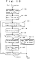
- Fig. 10 is a flowchart illustrating the operation of the input search processing 207 of Fig. 9 in greater detail.
- the present embodiment is intended to extract a state transition graph from the sequential circuit expressed in terms of logic elements, the state transition graph containing information about the operation.
- states of the sequential circuit are searched from an unknown initial state in the depth-first manner.
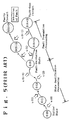
- Fig. 11 conceptually illustrates the search. This is known as a depth-first search and is a method of searching for one state which can be reached at the next time from a given state, and then a state that can be reached at the further next time can be explored from the searched state along a straight line.
- an input which maximises this evaluation function is searched at each instant of time.
- a nonlinear search method is introduced for this search. First, as given by Eqs. 1 and 2, the sequential circuit is formulated as a nonlinear system. Then, an input which maximizes the evaluation function is searched at each instant of time, by making use of information about the partial differential coefficient of the evaluation function with respect to the input. Since the information about the partial differential coefficient indicates the direction of the search for the input that maximizes the evaluation function, the number of trial searches can be reduced.
- the input-setting portion 9 is capable of distinguishing input bits which do not affect the pseudo-primary output at all. Therefore, when such input bits are present, the space in which inputs are being searched can be narrowed. Hence, the amount of calculation needed for the search can be reduced.
- the state transition graph generator of the present embodiment which essentially operates as described thus far is next described in further detail by referring to Figs. 8, 9, and 10.
- This state transition graph generator has two modes of operation. With respect to the second mode of operation, only those points which are different from the first mode of operation will be described.
- the initial value-setting portion 8 initializes the analog logic calculator portion 1 and the digital logic simulator 3 in such a way that the logic values of their flip-flops are unknown as given by Eqs. 8 and 9.
- x m (0) 0.0 where 1 ⁇ m ⁇ i (Eq. 8)
- x_logic m (0) 0 where 1 ⁇ m ⁇ i (Eq. 9)
- the initial value-setting portion 8 supplies all the bits of the input value u(0) ⁇ R j as - 1.0 indicating logic 0 to the signal line 101, initializes an amount of information P(-1) at a unit matrix, and sends it to the signal line 106.
- the state transition-managing portion 7 initialises all information about state transition in empty states.
- the differentiated value-calculating portion 2 calculates a Jacobian matrix of the pseudo-primary output value given by Eq. 3 with respect to the input value. The result is sent to the signal line 105.
- the input-setting portion 9 finds those input bits (hereinafter referred to as the invariable input bits) which do not affect the pseudo-primary output value from the Jacobian matrix output to the signal line 105.
- the invariable input bits make all elements of the corresponding partial differential coefficient assume value 0.0 (i.e., the sensitivity is zero), and this quality is utilized.
- the state transition-managing portion 7 stores the pseudo-primary output value x_logic(0), the pseudo-primary output value y_logic(0), and the input value u(0) as information regarding state transition at instant 0 output to the signal line 102.
- the information amount-calculating portion 4 performs the calculation given by Eq. 5, using the pseudo-primary output value y(t) supplied to the signal line 104, to calculate the amount of information P(t) at the time t. Furthermore, the calculating portion 4 outputs this amount P(t) to the signal line 106. This processing is equivalent to introducing the hysteresis of the pseudo-primary output value at the time t into the amount of information. Since the dimension of the amount of information P(t) is the bit number i of the flip-flops at most, the required storage capacity is very small.
- the times of the analog logic calculator portion 1 and of the digital logic simulator 3 are updated in accordance with Eqs. 11 and 12, respectively, so that t+1 is replaced by t.
- the analog logic calculator portion 1 updates the state, utilizing the pseudo-primary output value y_logic(t) of digital logic output to the signal line 112. Consequently, the nonlinear system follows the behavior of digital logic. This assures validity of search for inputs, making use of differential information.
- x_(t+1) y_logic(t) (Eq. 11)
- x_logic(t+1) y_logic(t) (Eq. 12)
- step 207 This is a step for searching for an input which maximizes the evaluation function (Eq. 6) at time t.
- the operation will be described in connection with step 301 and the following steps.
- the optimum input value u(t) determined as a result of the search is output to the signal line 101.
- the result of calculation of the pseudo-primary output value y(t) in response to the input value is output to the signal line 104.
- the digital logic simulator 3 executes a calculation given by Eq. 4, using the input value u(t) output to the signal line 101, and outputs the input value u(t), the pseudo-primary input value x_logic(t), and the pseudo-primary output value y_logic(t) to the signal line 102.
- the state transition-managing portion 7 stores the pseudo-primary input value x_logic(t), the pseudo-primary output value y_logic(t), and the input value u(t) as information regarding the state transition at the time t, the information being output to the signal line 102.
- the state transition-managing portion 7 determines from the information about the state transitions stored from time 0 to time t whether the following condition is satisfied; a transition to a completely novel state is not discovered when two or more transitions from the present state to the next state are made for every state which varied up to time t. If it is met, the entire operation is ended.
- Step 207 or the processing performed to search for inputs, will be described in detail with reference to Figs. 8 and 10.
- an input which maximizes the evaluation function (Eq. 6) at the time t is searched according to the partial differential coefficient of the evaluated value with respect to the input value.
- the input-setting portion 9 inverts about half of the bits of the input value u(t-1) ⁇ R j appearing at the immediately preceding time, the half bits having small absolute values of the partial differential coefficient, ⁇ J(t-1)/ ⁇ u(t-1) ⁇ R j at the immediately preceding time. Where j is an odd number, j is replaced by (j + 1)/2.
- the inverted bits are taken as an initial input value u0(t) and output to the signal line 101.
- invariable input bits are held at 0, indicating unknownness, and are extracted from the subjects of the above-described evaluation.
- the evaluated value-calculating portion 5 sets an initial evaluated value J0(t) at 0.
- the analog logic calculator portion 1 calculates a pseudo-primary output value y I (t) in accordance with Eq. 2, using the input value u I (t) ⁇ R j output to the signal line 101. The result is supplied to the signal line 104. All the values of the signal lines in the combinatorial circuit section of the sequential circuit are output to the signal line 103.
- the evaluated value-calculating portion 5 calculates an evaluated value J I (t) from the pseudo-primary output value y I (t) output to the signal line 104 and from the amount of information P(t-1) at the immediately preceding in accordance with Eq. 6, the amount of information being output to the signal line 106.
- the evaluated value-calculating portion 5 compares the evaluated value J I (t) calculated at step 304 with the evaluated value J I-1 (t) calculated in the immediately preceding loop. If J I (t) > J I-1 (t), control goes to step 306; otherwise control proceeds to step 309.
- the differentiated value-calculating portion 2 calculates a Jacobian matrix of the pseudo-primary output value with respect to the input value in accordance with Eq. 3, using every signal line value output to the signal line 103. The result is output to the signal line 105.
- all the elements of the Jacobian matrix for invariable input bits are taken as 0.0 and removed from the subjects of calculation.
- the evaluated value partial differential coefficient-calculating portion 6 calculates the partial differential coefficient ⁇ J I (t)/ ⁇ u I (t) ⁇ R j of the evaluated value in accordance with Eq. 7, using the data appearing at the signal line 105, the amount of information P(t-1) output to the signal line 106, and the pseudo-primary output value y I (t) output to the signal line 104. The result is output to the signal line 108.
- the partial differential coefficient of the evaluated value for invariable input bits is taken as 0.0 and removed from the subjects of calculation. Information regarding the calculated partial differential coefficient of the evaluated value indicates the direction of search for an input which maximizes the evaluation function.
- the amount of calculations for the Jacobian matrix given by Eq. 3 and for the partial differential coefficient of the evaluated value (Eq. 7) can be reduced.
- the input-setting portion 9 finds the following input value u I+1 (t) according to the rules described below, using the evaluated value partial differential coefficient ⁇ J I (t)/ ⁇ u I (t) ⁇ R j output to the signal line 108.
- the signs of the bits of the partial differential coefficient of the evaluated value and the signs of the bits of inputs are compared. If unlike signs are present, then the corresponding bits of inputs are inverted and taken as the next input value u I+1 (t). Also, these bits are output to the signal line 101.
- invariable input bits are not changed and are removed from the subject of evaluation. The invariable input bits are maintained at 0, indicating unknownness.
- the input-setting portion 9 compares the input value u I (t) and the next input value u I+1 (t) and determines whether a modification has been made (step 307). If it has been made, I + 1 is replaced by I, and control returns to step 303. If no modification has been made, the processing for searching for the input is ended.
- the input-setting portion 9 outputs the immediately preceding input value u I-1 (t) to the signal line 101.
- the analog logic calculator portion 1 computes a pseudo-primary output value y I-1 (t) in accordance with Eq. 2, using the input value u I-1 (t) ⁇ R j output to the signal line 101. The result is output to the signal line 104. Then, the processing for searching for the input is ended.
- the input-setting portion 9 used information about the Jacobian matrix given by Eq. 3 in distinguishing input bits which by no means affect the pseudo-primary output value. Instead, the partial differential coefficient of the evaluated value with respect to the input value as given by Eq. 7 can be used.
- the evaluation function serves to reduce the evaluated value on states different from states stored in the covariance matrix.
- a state transition graph can be created by searching for inputs so as to minimize this evaluated value.
- state transition graphs are searched by the depth-first method and, therefore, states which can be reached long after the initial state can be effectively searched well.
- the analog logic calculator portion 1 acts only to cause logic elements in the sequential circuit to take an analog form. In consequence, the storage capacity required for circuit conversion is much smaller than in the prior art techniques.
- the amount of information P(t) is a matrix having at most the dimension of the bit number of flip-flops, thus greatly reducing the storage capacity required. This makes it possible to create a state transition graph even for a sequential circuit having 2000 or more gates.
- states are searched by making use of the direction in which an evaluated value decreases most steeply with respect to the input value and so the amount of calculation needed for the search can be reduced.
- a state transition graph for a sequential circuit is extracted from an unknown initial state in the breadth-first manner.
- Fig.16 conceptually illustrates this embodiment.
- a breadth-first search is a method of searching for as many states as possible which can be reached at the next time from a given base state to extract a state transition graph, as illustrated in Fig. 16.
- This search method is carried out by establishing an evaluation function suitable for a search for states and searching for input values so as to minimize the evaluation function.
- the partial differential coefficient of the evaluated value with respect to the input value i.e., information regarding the direction of the steepest descent, is used.
- digital logic is made to assume an analog form by a nonlinear function.
- the evaluation function is based on the amount of information about the hysteresis of states stored in a covariance matrix and serves to reduce the evaluated values on states different from the stored states. Mathematically, where a state composed of plural bits is taken as a vector, states which are more closely perpendicular to the vector of the stored state have small evaluated values.
- the second embodiment of the novel state transition graph generator is nesting of three loops.
- the loop processing at the highest level is referred to as the first loop.
- the loop processing at the intermediate level is referred to as the second loop.
- the loop processing at the lowest level is referred to as the third loop. This type of loop processing is described successively with reference to Fig. 16.
- flip-flops of a sequential circuit start from an unknown state.
- the reached state is used as a base state.
- every state which can be reached from this base state is searched.
- a search for states from the base state ends, a search for states is repeated while employing the newly reached state as the next base state. This processing is continued until an access to a new base state is no longer possible. In this way, the first loop is processed for searching for states while repeatedly resetting a base state.
- a plurality of searches for states are performed with plural initial input values produced at random.
- Plural states which can be reached from one base state can be searched by repeating this loop.
- This loop is ended if access from the base state to a new state fails three times.
- Fig. 12 shows the structure of the state transition graph generator of the present embodiment. To simplify the illustration, only the differences with the first embodiment are described.
- An information amount-calculating portion 54 is a means for performing calculations to store the hysteresis of a pseudo-primary output value in a covariance matrix.
- the amount of information M(k) defined by a covariance matrix is defined by Eq. 13.
- M(k) M(k-1) + y(k)y t (k) (Eq. 13) where y(k) is a pseudo-primary output value, or state, calculated by the analog logic calculator portion, and k indicates the number of searches for inputs in the second loop of Fig. 16.
- An evaluated value-calculating portion 55 is a means for calculating an evaluated value J(k) in accordance with Eq. 14 from an amount of information M(k-1) and from a pseudo-primary output value y(k). This evaluated value decreases toward its minimum value as the difference between the hysteresis of the pseudo-primary output value stored in the amount of information M(k-1) and the pseudo-primary output value y(k) increases.
- J(k) y t (k)M(k-1)y(k) (Eq.
- An evaluated value partial differential coefficient-calculating portion 56 is a means for calculating the partial differential coefficient ⁇ J(k)/ ⁇ u(k) ⁇ R j of the evaluated value J(k) with respect to the input value u(k) in accordance with Eq. 15. Since this partial differential coefficient is in the direction of the steepest descent of the evaluated value with respect to the input value, the coefficient indicates the direction of search for an input which minimizes the evaluated value.
- An input-setting portion 59 is a means for estimating the direction of search for an input minimizing the evaluated value from the evaluated value partial differential coefficient output from the partial differential coefficient-calculating portion 56 and for searching for an input value that minimizes the evaluated value repeatedly.
- Signal lines 101-111, 506-510 interconnect the various blocks. Signals transmitted over these lines are described in detail in connection with the description of the operation of the invention.
- Figs. 13, 14, and 15 are flowcharts illustrating the operation of the state transition graph generator in the present embodiment, corresponding to the aforementioned first, second, and third types of loop processing.
- the operation of the second embodiment of the novel state transition graph generator constructed as described above will be described in detail with reference to Figs. 12, 13, 14, and 15.
- the state transition graph generator of the present embodiment has two modes of operation. With respect to the second mode of operation, only those points which differ from the first mode of operation will be described. First, the whole processing corresponding to the first loop is described with reference to Figs. 12 and 13.
- the initial value-setting portion 8 initializes the analog logic calculator portion 1, the digital logic simulator 3, and the state transition-managing portion 7.
- the initial value-setting portion 8 initializes the amount of information M(0) of the information amount-calculating portion 54 at 0 matrix.
- the amount of information M(0) is output to the signal line 506. This is processing for resetting the hysteresis of a state.
- the input-setting portion 59 outputs every bit of the input value u(0) ⁇ R j to the signal line 101 as - 1.0 indicating logic 0.
- the following processing is done only during second mode of operation.
- the next processing is performed to judge those input bits (invariable input bits) which do not affect the pseudo-primary output value. Invariable input bits make all the elements of the corresponding partial differential coefficients assume value 0.0, or sensitivity zero, and this quality is utilized.
- the differentiated value-calculating portion 2 calculates a Jacobian matrix of the pseudo-primary output value given by Eq. 3 with respect to the input value, and supplies the result to the signal line 105.
- Base search processing is performed. This processing is done to search for plural states which can be reached from a base state. The operation will be described in detail in connection with steps 701-707 described later.
- states which can be reached from an initial state are stored in the state transition-managing portion 7, together with input sequences leading to these states.
- the managing portion 7 determines whether a state not selected as a base state is present. If such a state is absent, the search for states is ended.
- the state transition-managing portion 7 outputs a state which has not been selected as a base state in the past to the signal line 102.
- the analog logic calculator portion 1 and the digital logic simulator 3 store the base state output to the signal line 102 in flip-flops.
- the amount of information is reset.
- the initial value-setting portion 8 resets the amount of information of the information amount-calculating portion 4 at 0 matrix (M(0)).
- An initial input value is set.
- An input value entered at the end of the immediately preceding search for base states is established as an initial input value u0(0) by the input-setting portion 59 which then supplies the set input value to the signal line 101.
- loop processing is performed successively, a number of loops k are used in the following description.
- this processing plural states which can be reached from a base state are searched, using plural initial input values produced at random.
- Input search processing is performed. This processing starts from the initial input value u0(k) and searches for one state which can be reached from a base state while repeatedly modifying an input value that minimizes the evaluated value. The operation will be described in detail in conjunction with steps 801-808 described later.
- the state transition-managing portion 7 compares the result of the search for states output to the signal line 102 and the hysteresis of the previously reached states stored in a table and determines whether a new state is reached. If it is reached, control goes to step 704. If it is not reached, control proceeds to step 705.
- the newly reached state is stored in a table within the state transition-managing portion 7.
- This managing portion 7 stores the state output to the signal line 102 and a search final input u(k) in the table.
- the pseudo-primary output value is stored in the amount of information.
- the information amount-calculating portion 54 stores the pseudo-primary output value y(k) output to the signal line 104 in the amount of information M(k) in accordance with Eq. 13.
- the next initial input value is set.
- the input-setting portion 59 sets the next initial input value u(k+1) at random. Control returns to step 702 after replacing k+1 with k.
- step 702 input search processing (step 702), corresponding to the third loop, is described with reference to Figs. 5 and 8.
- An initial evaluated value is set.
- the evaluated value-calculating portion 55 sets an initial evaluated value J ⁇ 1(k) to 10000.
- loop processing is initiated.
- An evaluated value for the input value u I (k) is calculated.
- the analog logic calculator portion 1 performs a calculation in accordance with Eq. 2, using the input value u I (k) supplied to the signal line 101.
- the calculated pseudo-primary output value y I (k) is supplied to the signal line 104. All signal line values in the sequential circuit are supplied to the signal line 103.
- the evaluated value-calculating portion 55 performs a calculation given by Eq. 14, using the pseudo-primary output value y I (k) supplied to the signal line 104 and the amount of information M(k-1) output to the signal line 506.
- the computed evaluated value J I (k) is supplied to the signal line 507.
- the evaluated value-calculating portion 55 compares the evaluated value J I (k) responsive to the input value u I (k) and the evaluated value J I-1 (k) responsive to the input value u I-1 (k) at the immediately preceding loop. If the evaluated value J I-1 (k) is less than the evaluated value J I (k), it follows that the evaluated value has been minimized at the (I-1)-th loop. If the latter is less than the former, control goes to step 804. If the former is less than the latter, control proceeds to step 807.
- the differentiated value-calculating portion 2 calculates a Jacobian matrix in accordance with Eq. 3, using the logic values of all signal lines output to the signal line 103. However, in the second mode of operation, the elements of the Jacobian matrix for invariable input bits are all 0.0 and are removed from the subjects of calculation. The result of the calculation is delivered to the signal line 105. Then, the partial differential coefficient-calculating portion 56 performs a calculation given by Eq. 15, using the Jacobian matrix output to the signal line 105 and the pseudo-primary output value y I (k) output to the signal line 104.
- the calculated partial differential coefficient of the evaluated value, or the direction of the steepest descent, is supplied to the signal line 508.
- the elements of the Jacobian matrix for invariable input bits are all 0.0 and are removed from the subjects of calculation. As described above, the amount of calculation is reduced in the second mode of operation.
- the input value is modified along the direction of the steepest descent (u I+1 (k)).
- the input-setting portion 59 finds the next input value u I+1 (k) according to the rules by making use of the direction of the steepest descent of the evaluated value responsive to the input value delivered to the signal line 508.
- Each bit of the input value u I+1 (k) is set to the direction of the sign indicated by the evaluated value partial differential coefficient, or the direction of the steepest descent. That is, if the sign is positive, the corresponding bit of the input value is set to -1.0. If the sign is negative, the corresponding bit is set to +1.0.
- the result is supplied to the signal line 101.
- invariable input bits are not changed and are removed from the subjects of evaluation. These invariable input bits are maintained at 0, indicating unknownness.
- the input-setting portion 59 compares the bits of the input value u I+1 (k) with the bits of the input value u I (k). If all of the compared bits agree precisely, then control goes to step 807. If different bits exist, then I+1 is replaced by I, and control returns to step 802.
- the input value u I-1 (k) to the immediately previous loop is established as the final input value u(k) in the search. This processing is done to search for the input value u I-1 (k), since the results of decisions made in steps 803 and 806 are that the evaluated value is minimized by the (I-1)th loop.
- the input-setting portion 9 outputs the input value u I-1 (k) to the signal line 101.
- the analog logic-calculating portion 1 performs a calculation given by Eq. 2, using the input value u I-1 (k) supplied to the signal line 101.
- the result of the calculation, or the pseudo-primary output value y(k) is supplied to the signal line 104.
- the digital logic simulator 3 is driven with the final input value u(k) in the search to calculate actual digital logic values.
- the simulator 3 performs a digital logic calculation given by Eq. 4, using the final input signal u(k) in the search, the signal being delivered to the signal line 101.
- the final input value u(k) and the reached state y logic(k) are output to the signal line 102.
- the processing for searching for inputs is ended.
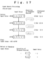
- Fig. 17 illustrates one example of the execution of input search processing, and indicates a procedure for searching for an input that minimizes the evaluated value while changing the input value from the initial value u0(k) in the steepest descent.
- u2(k) is selected as the final input value u(k), because the input value was not changed in step 806 when a change from u2(k) to u3(k) was made. Since input values are searched while utilizing information regarding the direction of the steepest descent of the evaluated value in this way, the amount of calculation needed for the search can be reduced.
- a state transition graph is searched by a breadth-first method. Therefore, states which can be reached from an initial state in a short time can be efficiently searched.
- the storage capacity needed for circuit conversion and for searches for states can be reduced, in exactly the same way as in the first embodiment.
- a third embodiment of the novel state transition graph generator is described below.
- the third embodiment differs from the second embodiment in terms of its method of setting an evaluation function. The concept thereof is described below.
- Fig. 18 shows the structure of the third embodiment of the novel state transition graph generator.
- the third embodiment differs from the second embodiment in that a division information amount-calculating portion 1104 and a division evaluated value-calculating portion 1105 are added and that an evaluated value partial differential coefficient-calculating portion 1106 performs a different calculation.
- the flow of operation is exactly the same as the flow of Figs. 13,14 and 15. Therefore, only those points of structure which are different from the second embodiment are described; the operation thereof will not be described.
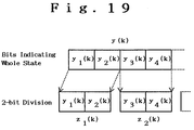
- the division information amount-calculating portion 1104 is a means for performing calculations to divide the pseudo-primary output value in units of 2 bits and to store them in separate covariance matrices.
- a calculational formula is indicated in Eq. 16.
- D j (k) is an amount of information for dividing bits indicating states in units of 2 bits and storing them in separate covariance matrices, and j indicates a division number.
- This information amount D j (k) is information which sees states locally.
- D j (k) D j (k-1) + z j (k)z j t (k) ) (Eq. 16) where z j (k) indicates each state divided in units of 2 bits (see Fig. 19).
- the division evaluated value-calculating portion 1105 calculates an evaluated value J2(k) in accordance with Eq. 17 from an amount of information D j (k-1) and from a pseudo-primary output value y(k). Also, the calculating portion 1105 calculates an evaluated value J(k) in accordance with Eq. 18, the value J(k) being defined as a linear sum of an evaluated value J1(k) based on the amount of information M(K) output from the evaluated value-calculating portion 5 and the above evaluated value J2(k).
- J1(k) corresponds to an evaluated value which sees states as a whole.
- J2(k) corresponds to an evaluated value which sees states locally.
- the evaluated value partial differential coefficient-calculating portion 1106 is a means for calculating the partial differential coefficient ⁇ J(k)/ ⁇ u(k) ⁇ R j of the evaluated value J(k) with respect to the input value u(k) in accordance with Eq. 19. This coefficient indicates the direction of the steepest descent of the evaluated value with respect to the input value.
- the evaluation function serves to reduce evaluated values on states which differ from the state stored in a covariance matrix. Input values are searched so as to minimize this evaluated value.
- a state transition graph can be created.
- the storage capacity necessary for circuit conversion and search for states and the amount of calculation necessary for the search for states can be reduced, in exactly the same way as in the second embodiment.
- FIG. 22 conceptually illustrates a case in which the depth-first search described in the first embodiment for creating a state transition graph is used as a state transition graph generator means.
- Fig. 23 conceptually illustrates a case in which the breadth-first search described in the above-described second and third embodiments is employed.
- a state transition graph is created, using a fault-free sequential circuit, by any one of the above-described embodiments of the state transition graph generator.
- This corresponds to state justification processing in generating a test pattern. That is, a test pattern for states which can be reached from an arbitrary state is previously created. Then, one fault type is selected. After the selection, fault propagation processing for the fault type is performed by the RTP method to search for a fault excitation state. If the fault propagation processing fails, an input sequence created during the unsuccessful process is taken as a test pattern. If it succeeds, state justification processing is initiated. More specifically, whether a fault excitation state is contained in states which are reached by the state transition graph generator is determined. If such a state is present, the test pattern leading to the fault excitation state and the test pattern generated by the fault propagation processing are connected together, and a test pattern for the fault-excited type is generated.
- Fig. 20 shows the structure of the first embodiment of the novel test pattern generator.
- a state transition graph generator 1301 consists of the novel state transition graph generator described above.
- Components 2501-2504, 2506-2508 are exactly the same as their counterparts of the test pattern generator utilizing the RTP method described in connection with the prior art techniques and so detailed description of them is omitted.
- Fig. 21 is a flowchart illustrating the operation of the first embodiment of the novel test pattern generator.
- the state transition graph generator 1301 creates a state transition graph for a fault-free circuit in the manner as described already in connection with embodiments of the state transition graph generator.
- the fault type-managing table 2501 performs a check as to whether unsearched fault types exist. If they do not exist, the processing for generating a test pattern is ended.
- the fault type-managing table 2501 selects one out of fault types which are neither detected nor searched.
- the fault propagation processing portion 2502 performs fault propagation processing for the fault type selected in step 1403 by the RTP method.
- the generated test pattern is output to the propagation sequence storage table 2505.
- the fault propagation processing portion 2502 performs a check as to whether fault propagation processing has been done successfully. If it succeeds, a fault excitation state is delivered to the fault excitation state buffer 2504, and control goes to step 1406. If it fails, control jumps to step 1407.
- the state transition-managing portion 7 performs a check to see if the fault excitation state stored in the fault excitation state buffer 2504 is contained in the states reached by the state transition graph created in step 1401. If it is contained therein, the managing portion 7 stores a test pattern leading from an arbitrary initial state to the coincident state in the justification sequence storage table 2506.
- test pattern created for the fault type selected in step 1403 is loaded into the test pattern-managing table 2508. Specifically, test patterns stored in the propagation sequence storage table 2505 and in the justification sequence storage table 2506 are loaded in the order of state justification sequence and fault propagation sequence.
- the fault simulator 2507 makes a simulation of a fault, using the test pattern created for the fault type selected in step 1403. Then, information regarding the newly detected fault type is sent to the fault type-managing table 2501. Finally, the propagation sequence storage table 2505 and the justification sequence storage table 2506 are cleared. Control then goes back to step 1402.
- the fault propagation processing portion 2502 can repeat the fault propagation processing while varying the method of searching to detect different fault excitation states.
- state justification processing is performed for the fault excitation state generated by the RTP method, by making use of the novel state transition graph generator. This improves the performance of the state justification processing and thus improves the fault coverage.
- FIG. 26 conceptually illustrates a case in which the depth-first search described previously in connection with the first embodiment of the state transition graph generator is used as a state transition graph generator means.
- Fig. 27 conceptually illustrates a case in which the breadth-first search described already in connection with the second and third embodiments of the generator is employed.
- a state transition graph is created, using a fault-free sequential circuit, by any one of the above-described embodiments of the novel state transition graph generator.
- states which can be reached from an arbitrary initial state and test patterns leading to these states are found.
- one fault type is selected.
- fault propagation processing for the fault type is performed by the RTP method to search for a fault excitation state. If the fault propagation processing fails, an input sequence created during the unsuccessful process is taken as a test pattern. If it succeeds, state justification processing is performed in the manner described now. First, whether the found fault excitation state S(9) is contained in the states reached by the state transition graph generator is determined.
- test pattern leading to the fault excitation state and the test pattern generated by the fault propagation processing are connected together to create a test pattern. If such a state is not contained therein, state justification processing is done for one unit period of time by the RTP method. Then, whether a target state S(8) found by the RTP method by going back to the immediately preceding time is one of the states reached by the state transition graph generator is determined. In this way, state is justified while performing a check as to whether the target state undergoing state justification processing by the RTP method is coincident with any one of the states within the state transition graph. For example, Fig. 27 shows a case in which a target state S(7) agrees with any one of the states within the state transition graph.
- Fig. 24 shows the structure of the second embodiment of the novel test pattern generator.
- a state justification processing portion 2503 is exactly the same as the corresponding component of the test pattern generator using the RTP method as already described in conjunction with the prior art techniques.
- the second embodiment differs from the first embodiment in that the state justification processing portion 2503 is added as a component and that the fault excitation state buffer 2504 receives inputs from the fault propagation-processing portion 2502 and also from the state justification processing portion 2503.
- Fig. 25 is a flowchart specifically illustrating the state justification processing (step 1406).
- step 1408 in addition to the operation described in connection with the first embodiment, the state of a fault-free circuit after making a simulation of a fault is supplied to the state justification processing portion.
- the state transition-managing portion 7 determines whether the target state (a fault excitation state in the first operation) loaded in the fault excitation state buffer 2504 is contained in the states reached by the state transition graph. If the target state is contained therein, the managing portion 7 loads a test pattern leading to the coincident target state from an arbitrary initial state into the justification sequence storage table 2506. Thus, the state justification processing is ended.
- the state justification processing portion 2503 performs state justification processing corresponding to one unit period of time by the RTP method.
- the generated inspection input is delivered to the justification sequence storage table 2506.
- the state justification processing portion 2503 determines whether the justification of state has been successfully performed. If it succeeds, the test pattern which is loaded in the justification sequence storage table 2506 and leading to a fault excitation state from an initial state is a state justification sequence. Thus, the state justification processing is ended.
- the initial state at this time is the state of the fault-free circuit after driving the fault simulator 2507 in step 1808.
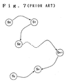
- the state justification processing portion 2503 determines whether the processing for justifying states should be interrupted. This interruption occurs when the situation described in the description of the problems to be solved by the invention (Figs. 6 and 7) occurs.
- the state justification processing portion 2503 loads the target state (such as S(8) in Fig. 27) presently undergoing state justification processing into the fault excitation state buffer 2504. Control then goes back to step 1801.
- target state such as S(8) in Fig. 27
- the fault propagation processing portion 2502 may change the method of search, repeat the fault propagation processing, and search for different fault excitation states.
- state justification processing is performed by utilizing the RTP method and the above-described novel state transition graph generator in a complementary manner and, therefore, the performance of the state justification processing is improved. This can improve the fault coverage.
- a third embodiment of the novel test pattern generator is described below.
- This third embodiment utilizes the aforementioned method of creating a state transition graph as processing subsequent to the test pattern generator making use of the RTP method. That is, after the test pattern generator based on the RTP method creates a test pattern once, additional inspection inputs are created for fault types which cannot be detected.
- This concept of generating inspection inputs is exactly the same as the concept of the first embodiment. The concept is illustrated in Figs. 22 and 23, and is described below.
- a state transition graph is created, using a fault-free sequential circuit of any one of the above-described embodiments of the state transition graph generator.
- This corresponds to state justification processing in generating a test pattern. That is, a test pattern leading to a state which can be reached from an unknown initial state is previously created. Then, one undetected fault type is selected. Subsequently, fault propagation processing for the fault type is performed by the RTP method. If the fault propagation processing fails, the generation of an inspection input for that fault type is interrupted. If the processing succeeds, the process goes to state justification processing. More specifically, a check is performed to see if a fault excitation state is contained in the state reached by the state transition graph generator. If it is contained therein, the test pattern leading to the fault excitation state and the test pattern generated by the fault propagation processing are connected together to create a test pattern for the fault type.
- Fig. 28 shows the structure of the third embodiment of the novel test pattern generator.
- an undetected fault type-managing table 1302 manages fault types which remain undetected when test patterns are created by the use of a fault propagation processing portion 2502 and a state justification processing portion 2503.
- the difference of the third embodiment from the first embodiment of the invention is that the state justification processing portion 2503 and the undetected fault type-managing table 1302 are added as components.
- Fig. 29 is a flowchart illustrating the operation of the third embodiment of the novel test pattern generator.
- Test patterns are created, using the fault propagation processing portion 2502 and the state justification processing portion 2503. Detailed operation for the processing is exactly the same as the operation already described in the item of the prior art techniques. As a result, fault types left undetected are stored in the undetected fault type-managing table 1302.
- the undetected fault type-managing table 1302 performs a check to see if undetected fault types are present. If they not present, the processing for generating test patterns is ended.
- the state transition graph generator 1301 creates a state transition graph for a fault-free circuit.
- the operation for creating a state transition graph is the same as the operation described previously in the embodiments of the novel state transition graph generator.
- the following operation is a processing involving loops corresponding in number to the undetected fault types.
- the undetected fault type-managing table 1302 performs a check to see if undetected fault types are present. If they not present, the processing for generating test patterns is ended.
- the undetected fault type-managing table 1302 selects one from among the undetected fault types.
- the fault propagation processing portion 2502 performs fault propagation processing for the selected fault type.
- the resulting fault propagation sequence is loaded into the propagation sequence storage table 2505.
- the fault propagation processing portion 2502 performs a check to see if the fault propagation processing is successfully performed. If successful, the fault excitation state is loaded into the fault excitation state buffer 2504. If unsuccessful, the propagation sequence storage table 2505 is reset, and control returns to step 2204.
- the state transition-managing portion 7 performs a check to see if the fault excitation state loaded in the fault excitation state buffer 2504 is contained in the states reached by the state transition graph created in step 2203. If it is contained therein, the managing portion 7 loads a test pattern leading from an arbitrary initial state to the coincident fault excitation state into the justification sequence storage table 2506. If it is not contained therein, the table 2505 is reset, and control goes back to step 2204.
- Test patterns loaded in the justification sequence storage table 2506 and in the propagation sequence storage table 2505 are loaded into the test pattern-managing portion 2508 in that order. Control returns to step 2204.
- test patterns in the third embodiment of the novel test pattern generator will be described.
- a state transition graph generator the generator described in the third embodiment described above is used. Used sequential circuits are some of the benchmark circuits described in Proc. of Int. Symp. Circuit and Systems (1989), pp. 1929-1934 (ISCAS' 89). Fault coverages are listed in Table 1. For comparison, fault coverages obtained only by the prior art techniques are also listed. Table 1 circuit name fault coverage according to the invention fault coverage according to prior art techniques s298 85.71% 84.42% s344 95.91% 92.42% s382 91.23% 87.97% s444 89.03% 86.29% s1494 93.89% 93.16%
- the fault propagation processing portion 2502 performs fault propagation processing for undetected fault types in step 2206. It is also possible to provide a means for holding information regarding fault propagation processing when test patterns are generated in step 2201 and to omit this processing. Furthermore, in step 2206, the fault propagation processing portion 2502 may also vary the method of search to perform fault propagation processing different from the processing of step 2201, to search for a different fault excitation state.
- the various means and simulators used in the present invention may be realized by software used in a computer. Also, they may be realized using dedicated hardware circuits having the same functions.
- the present invention defines an evaluation function which can take an optimum evaluated value when a pseudo-primary output value or state is different from the hysteresis observed in the past. Therefore, the problem of finding a state transition graph can be concluded in the problem of maximization of this evaluation function.
- This evaluation function is based on an amount of information defined in terms of a square matrix having only a dimension of the number of bits of flip-flops, the amount of information being given by Eq. 5. Therefore, almost no storage capacity is needed.
- test pattern generator In the present test pattern generator described above, the performance of the state justification processing can be improved compared with the prior art RTP method. This test pattern generator has an excellent fault coverage.
Landscapes
- Engineering & Computer Science (AREA)
- Physics & Mathematics (AREA)
- General Engineering & Computer Science (AREA)
- General Physics & Mathematics (AREA)
- Computer Hardware Design (AREA)
- Theoretical Computer Science (AREA)
- Evolutionary Computation (AREA)
- Geometry (AREA)
- Test And Diagnosis Of Digital Computers (AREA)
Applications Claiming Priority (4)
| Application Number | Priority Date | Filing Date | Title |
|---|---|---|---|
| JP159844/92 | 1992-06-18 | ||
| JP15984492 | 1992-06-18 | ||
| JP25779692 | 1992-09-28 | ||
| JP257796/92 | 1992-09-28 |
Publications (2)
| Publication Number | Publication Date |
|---|---|
| EP0574919A2 true EP0574919A2 (fr) | 1993-12-22 |
| EP0574919A3 EP0574919A3 (fr) | 1998-01-21 |
Family
ID=26486520
Family Applications (1)
| Application Number | Title | Priority Date | Filing Date |
|---|---|---|---|
| EP93109708A Withdrawn EP0574919A3 (fr) | 1992-06-18 | 1993-06-17 | Générateur de diagramme de transition d'état et générateur de configurations de test |
Country Status (1)
| Country | Link |
|---|---|
| EP (1) | EP0574919A3 (fr) |
Cited By (3)
| Publication number | Priority date | Publication date | Assignee | Title |
|---|---|---|---|---|
| EP0529670B1 (fr) * | 1991-08-30 | 1997-06-04 | Matsushita Electric Industrial Co., Ltd. | Appareil de génération de configurations de test |
| US20130278500A1 (en) * | 2010-12-17 | 2013-10-24 | Gifu University | Side-type force sense interface |
| CN113900423A (zh) * | 2021-08-31 | 2022-01-07 | 北京空间飞行器总体设计部 | 一种基于fsm的火星车休眠唤醒功能验证方法 |
Family Cites Families (2)
| Publication number | Priority date | Publication date | Assignee | Title |
|---|---|---|---|---|
| EP0342787A3 (fr) * | 1988-04-15 | 1991-03-27 | AT&T Corp. | Procédé de recherche pour la génération de vecteurs de test pour circuits logiques séquentiels |
| JPH05273310A (ja) * | 1991-08-30 | 1993-10-22 | Matsushita Electric Ind Co Ltd | 検査系列生成装置 |
-
1993
- 1993-06-17 EP EP93109708A patent/EP0574919A3/fr not_active Withdrawn
Cited By (5)
| Publication number | Priority date | Publication date | Assignee | Title |
|---|---|---|---|---|
| EP0529670B1 (fr) * | 1991-08-30 | 1997-06-04 | Matsushita Electric Industrial Co., Ltd. | Appareil de génération de configurations de test |
| US20130278500A1 (en) * | 2010-12-17 | 2013-10-24 | Gifu University | Side-type force sense interface |
| US9189065B2 (en) * | 2010-12-17 | 2015-11-17 | Gifu University | Side-type force sense interface |
| CN113900423A (zh) * | 2021-08-31 | 2022-01-07 | 北京空间飞行器总体设计部 | 一种基于fsm的火星车休眠唤醒功能验证方法 |
| CN113900423B (zh) * | 2021-08-31 | 2023-07-14 | 北京空间飞行器总体设计部 | 一种基于fsm的火星车休眠唤醒功能验证方法 |
Also Published As
| Publication number | Publication date |
|---|---|
| EP0574919A3 (fr) | 1998-01-21 |
Similar Documents
| Publication | Publication Date | Title |
|---|---|---|
| US5485471A (en) | System for testing of digital integrated circuits | |
| US5568203A (en) | Apparatus for estimating real-time motion an a method thereof | |
| EP0726538A2 (fr) | Système pour la CAO de circuits digitaux, basé sur leur topologie et méthode correspondante | |
| US5461573A (en) | VLSI circuits designed for testability and methods for producing them | |
| EP3889843A1 (fr) | Dispositif et procédé d'optimisation | |
| US5491639A (en) | Procedure for verifying data-processing systems | |
| JPH05113468A (ja) | 検査系列生成方法 | |
| US5996101A (en) | Test pattern generating method and test pattern generating system | |
| US6408424B1 (en) | Verification of sequential circuits with same state encoding | |
| US5586125A (en) | Method for generating test vectors for characterizing and verifying the operation of integrated circuits | |
| US20050149804A1 (en) | Device and method for testing integrated circuit | |
| US5968195A (en) | Estimation of failure section region with small simulation calculation quantity | |
| EP0574919A2 (fr) | Générateur de diagramme de transition d'état et générateur de configurations de test | |
| US6678739B1 (en) | System, method, and computer program product for compressing test pattern set | |
| KR100317543B1 (ko) | 테스트용이화설계방법과장치,정보기억매체및집적회로장치 | |
| US5526514A (en) | Method for circuit verification and multi-level circuit optimization based on structural implications | |
| JP2865136B2 (ja) | テスト考慮論理合成システム | |
| EP0529670A2 (fr) | Appareil de génération de configurations de test | |
| US6223316B1 (en) | Vector restoration using accelerated validation and refinement | |
| Viktoros et al. | Compact fault dictionaries for efficient sensor fault diagnosis in IoT-enabled CPSs | |
| US6651206B2 (en) | Method of design for testability, test sequence generation method and semiconductor integrated circuit | |
| US6877141B2 (en) | Evaluating a validation vector for validating a network design | |
| US20030188239A1 (en) | Compacted test plan generation for integrated circuit testing, test sequence generation, and test | |
| US7120829B2 (en) | Failure propagation path estimate system | |
| Chen et al. | Diagnostic fault simulation for synchronous sequential circuits |
Legal Events
| Date | Code | Title | Description |
|---|---|---|---|
| PUAI | Public reference made under article 153(3) epc to a published international application that has entered the european phase |
Free format text: ORIGINAL CODE: 0009012 |
|
| AK | Designated contracting states |
Kind code of ref document: A2 Designated state(s): DE FR GB |
|
| RAP1 | Party data changed (applicant data changed or rights of an application transferred) |
Owner name: MATSUSHITA ELECTRIC INDUSTRIAL CO., LTD. |
|
| PUAL | Search report despatched |
Free format text: ORIGINAL CODE: 0009013 |
|
| AK | Designated contracting states |
Kind code of ref document: A3 Designated state(s): DE FR GB |
|
| STAA | Information on the status of an ep patent application or granted ep patent |
Free format text: STATUS: THE APPLICATION IS DEEMED TO BE WITHDRAWN |
|
| 18D | Application deemed to be withdrawn |
Effective date: 19980722 |