EP0574986A1 - Datenverarbeitungsvorrichtung mit einer Prozessorarchitektur für Einzelbefehle und Mehrfachdaten - Google Patents
Datenverarbeitungsvorrichtung mit einer Prozessorarchitektur für Einzelbefehle und Mehrfachdaten Download PDFInfo
- Publication number
- EP0574986A1 EP0574986A1 EP93201645A EP93201645A EP0574986A1 EP 0574986 A1 EP0574986 A1 EP 0574986A1 EP 93201645 A EP93201645 A EP 93201645A EP 93201645 A EP93201645 A EP 93201645A EP 0574986 A1 EP0574986 A1 EP 0574986A1
- Authority
- EP
- European Patent Office
- Prior art keywords
- data
- scalar
- elementary
- processor
- processors
- Prior art date
- Legal status (The legal status is an assumption and is not a legal conclusion. Google has not performed a legal analysis and makes no representation as to the accuracy of the status listed.)
- Granted
Links
Images



Classifications
-
- G—PHYSICS
- G06—COMPUTING OR CALCULATING; COUNTING
- G06F—ELECTRIC DIGITAL DATA PROCESSING
- G06F15/00—Digital computers in general; Data processing equipment in general
- G06F15/76—Architectures of general purpose stored program computers
- G06F15/80—Architectures of general purpose stored program computers comprising an array of processing units with common control, e.g. single instruction multiple data processors
- G06F15/8007—Architectures of general purpose stored program computers comprising an array of processing units with common control, e.g. single instruction multiple data processors single instruction multiple data [SIMD] multiprocessors
- G06F15/8015—One dimensional arrays, e.g. rings, linear arrays, buses
Definitions
- the invention relates to a data processing device comprising a plurality of elementary processors operating in parallel in a so-called common instruction mode acting on multiple data with a plurality of output data buses, means for collectively processing multiple data of output, with a common input control bus and a common input data bus.
- a device provided with such an architecture makes several processors operate simultaneously on different data using a single command and outputs several results (this mode is called SIMD in English).
- Highly parallel architectures of this type are used in particular in neural networks.
- the document EP 0 322 966 describes a neural network whose architecture can be broken down into several elementary processors each having a part of the memory of synaptic coefficients C ij , a state register of neurons V i and means for calculating of contributions C ij .V i . All these elementary processors share a common input bus and deliver in parallel output a plurality of contributions C ij .V i which are added in a tree of adders.
- Devices of this type are designed so that the data follows a direct path (flow) between the input and the output.
- This type of architecture is intended to increase the speed of execution of such data processing devices. They are therefore designed to manage data streams which follow parallel paths going from the input to the output of said device with maximum speed. During these parallel journeys, the data flows remain independent until they are grouped together to be collectively added, compared or otherwise.
- neural networks in particular are implementing treatments which are becoming more and more sophisticated with increasingly diverse applications using increasingly complex algorithms.
- a neural network having a determined material structure must have an extensive set of instructions which allows it to process a maximum of applications and therefore algorithms dedicated to each of these applications.
- data streams following exclusively parallel paths do not make it possible to deal with interactions between these streams during their hitherto independent processing.
- the object of the invention is therefore to break with this exclusive independence of parallel paths, therefore of processing, by making it possible to introduce modular interactions between flows.
- each elementary processor comprises input means and / or output means, an identification member which activates said means when an identification signal is received by said processor, said device further comprising a scalar-vector control unit (SVCU ) which, in response to said identification signal, authorizes said elementary processor either to receive or to deliver scalar data.
- SVCU scalar-vector control unit
- the data processing device can be provided with a scalar-scalar transformation unit SSU which receives a scalar result from the vector-scalar transformation unit VSU.
- the scalar-scalar transformation unit SSU can deliver said common scalar datum.
- Each elementary processor is provided with a local memory to store synaptic coefficients and / or states of neurons.
- the memory is organized in a stack of registers which stores synaptic coefficients and states of neurons, by storing either predominantly synaptic coefficients or predominantly states of neurons.
- the reading of the memory is preferably dual access in order to access both the synaptic coefficients and the states of neurons, which increases the speed of execution.
- Synaptic coefficients can be stored in memory according to a so-called diagonal arrangement.
- a matrix of synaptic coefficients C ij into a transposed matrix of synaptic coefficients C ji .
- This possibility is used in particular in the implementation of the error backpropagation algorithm during learning phases implemented in a neural network.
- FIG. 1 represents a simplified architecture known from a machine with a SIMD architecture.
- a plurality of elementary processors P1 ... Pn each provided with a local memory, all receive in parallel, at a given instant, the same instruction coming from a control unit 10.
- This common instruction is distributed to all processors by a common control bus IC. All processors thus perform the same task at the same time. But this same task can be performed on data that is generally different.
- the data that receive the elementary processors P1 ... Pn come from a block 11 of common resources. These data are distributed sequentially or not by a data bus ID.
- all the processors can carry out at the same time an operation of adding data placed on the bus ID with each of the results stored in each processor. It can also be a series of data placed on the ID bus, each with a serial number which is recognized individually by each processor.
- each elementary processor takes the data which concerns it in said data series and performs the programmed common operation.
- the plurality of elementary processors thus each delivers an individual result on their outputs OUT1 ... OUTn.
- a mechanism is for example implemented in image processing in which each elementary processor is assigned to the individual processing of a pixel of the image.
- the outputs OUT1 - OUTn thus deliver a series of results independent of each other.
- FIG. 2 represents the architecture of a part of a data processing device according to the invention, said architecture highlighting interactions between the data streams implemented in and / or by elementary processors which operate in SIMD mode.
- the plurality of elementary processors EP1 - EPn receives as input instructions from a control bus IC and data from a data bus ID.
- Each elementary processor delivers a result on an individual output bus OB1 - OBn through output means 171 - 17 n . So that each elementary processor can communicate with its closest neighbors, each elementary processor is provided with communication means 151 - 15 n which make it possible to transfer data on a chained path DP. It is thus possible to transfer data step by step to the other elementary processors.
- These data exchanges can relate to any data contained in the elementary processor.
- each elementary processor is no longer independent. This is particularly useful when the contribution provided by an elementary processor is associated with the contributions provided by the other processors.
- the plurality of elementary processors EP1 - EPn constitutes a vector processor VP which delivers a plurality of results forming a vector result.
- the latter is then processed globally by a vector-scalar unit VSU which transforms the result of vector type into a result of scalar type.
- a situation of this type is for example encountered when said device is a neural processing device. It is then possible for the processors to communicate for example states of neurons V i , synaptic coefficients C ij or contributions C ij .V j .
- a particularly interesting situation concerns the transposition of a matrix of synaptic coefficients C ij into a transposed matrix C ji .
- the invention takes advantage of a particular arrangement of the synaptic coefficients in the local memories of the elementary processors in order to be able to easily deduce the transposed matrix C ji from the direct matrix C ij .
- This arrangement consists in storing the data no longer in the form of lines (or columns) of a memory addressed by a row / column addressing, but in arranging the synaptic coefficients according to a diagonal of the memory.
- column addressing continues to address columns of the memory but row addressing then addresses diagonals (or more exactly parallels to the diagonals) of the memory.
- Another choice allows you to reverse the two types of addressing.
- the unit VSU can thus determine a scalar quantity equal to the sum of the contributions C ij .V i delivered by each processor or to the sum of the contributions C ji .V j in the case of the transposed matrices. This is used in the so-called learning mode of a neural network during the implementation of the algorithm. backpropagation of errors.
- the means of communication 15 are not limited to the permutations of the synaptic coefficients and can be used for other data in the case of neural networks or in the case where the combination of elementary processors forms another machine which requires interaction. Between them data flows from elementary processors. It may for example be a processing device which operates digital filtering processing. A series of samples x1 - x n is distributed in the n elementary processors by a serial loading through the chained path DP. The filter weights are stored in the local memory of each processor. The elementary contributions determined in each elementary processor are combined in the unit VSU.
- FIG. 3 represents a particular embodiment of the invention. Indeed, it may also be desirable for certain applications for each elementary processor to be able to communicate with other elementary processors through the common data bus ID. This is for example the case when an elementary processor needs to communicate a data to all or certain other elementary processors.
- a processor can calculate a local maximum (minimum) that is passed to other processors to determine an overall maximum (or minimum).
- each elementary processor comprises output means 19 which put on the input bus ID at least one scalar datum. This setting of the data on the bus is controlled by an SVCU control unit which activates only one processor at a time. This command can act individually on each elementary processor thanks to an identifier stored in an identification circuit 16 disposed in each elementary processor which receives an identification signal SI.
- each elementary processor contains input means 13 which allow either selectively or collectively to enter into the elementary processors the data placed on the input bus ID.
- the input means 13 are then also controlled by the control unit SVCU and the identification signal SI. So we can distribute on all the elementary processors the same scalar data: this operation is similar to a scalar-vector transformation.
- the SVCU unit then acts as a scalar-vector transformation unit.
- the data thus put on the bus ID can not only come from the output means 19 but also come from another source.
- the scalar result delivered by the VSU unit is processed by an SSU unit which transforms the scalar result into another scalar result.
- the latter can then be looped back to the ID bus to be redistributed selectively or collectively on the elementary processors. This loop operation process is implemented in certain processing phases of a neuron network.
- the index b is assigned to the elementary processor shown in FIG. 4 and the indices a and c are assigned to the registers 15 belonging to the adjacent elementary processors placed respectively upstream and downstream.
- the register 15b is doubled by a register 15'b.
- the output 25'b of the register 15'b is then connected to the register 15'a of the preceding elementary processor if the output 25b of the register 15b is connected to the following elementary processor.
- the output of register 15'c of the following processor is then connected to the input of multiplexers 221 and 222.
- the register 15'b is shown in bold dashed lines to indicate that it is optional, and the registers 15a and 15'c are shown in thin dashed lines to indicate that they belong to adjacent elementary processors.
- the memory 26 is preferably a dual read access memory. It is thus possible to read in the memory two types of data intended to be available at the same time, respectively on the two inputs of the ALU.
- One type of data can for example be constituted by states of neurons and the other type of data can then be constituted by synaptic coefficients.
- the same neuron state is to be associated with several synaptic coefficients or vice versa, for this purpose it is possible to store in memory 26 mainly synaptic coefficients or mainly neuron states or store them in equal quantities.
- the data processing device as a whole and each elementary processor in particular has to update synaptic coefficients and states of neurons.
- These updated data, originating from the multiplexer 24, are therefore rewritten (connection 27) in the memory 26 during the course of the processing operations.
- the link interface preferably comprises two analog blocks LINK1 and LINK2 which can communicate (L1 and L2) in bidirectional mode with the outside world.
- the DMA block includes a counter which generates addresses 321 - 32 n for each local memory RGF of each elementary processor to extract or place on the bus ID data passing from the interior to outside the DSP device or vice versa.
- the control block 30 supplies the control signals to the different units from the instructions or addresses received on the I / A bus.
- the DSP data processing device can be used in several ways without changing either its design or its architecture.
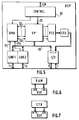
- FIG. 6 shows an autonomous mode of operation.
- the DSP device is connected to an external RAM memory. They communicate via the I / A bus, the DSP device receiving INS instructions from the RAM on a part of the I / A bus, for example 16 bits, and sending ADR addresses to the RAM memory to obtain following instructions on the other part of the I / A bus, for example 16 bits.
- FIG. 7 represents an operating mode where the DSP device is connected to an external controller CTR.
- the I / A bus is then used in full (32 bits) to provide instructions to the DSP device, the I / A bus being divided into most significant bits MSB and least significant bits LSB.
- a device DSP1 can on the one hand receive on its bus I (16 bits) data coming from the bus O (16 bits) of a device DSP2, and it can on the other hand deliver on its bus O (16 bits ) data on the I bus (16 bits) of a DSP3 device.
- Interconnection can also be done via the LINK1 / LINK2 link interfaces ( Figure 9).
- a DSP1 device can on the one hand bidirectionally exchange data with a DSP2 device via their L1 bus and on the other hand bidirectionally exchange data with a DSP3 device through their L2 bus.
- a DSP device can also be connected ( Figure 10) to an external scalar processor or to a storage table for LUT data, bus I of one being connected to bus O of the other.
- a DSP device can be connected to a backup memory MEM (FIG. 11).
- the L1 buses connected together ensuring a direction of communication and the L2 buses connected together ensuring the other direction of communication.
Landscapes
- Engineering & Computer Science (AREA)
- Computer Hardware Design (AREA)
- Theoretical Computer Science (AREA)
- Computing Systems (AREA)
- Physics & Mathematics (AREA)
- General Engineering & Computer Science (AREA)
- General Physics & Mathematics (AREA)
- Multi Processors (AREA)
- Complex Calculations (AREA)
Applications Claiming Priority (2)
| Application Number | Priority Date | Filing Date | Title |
|---|---|---|---|
| FR9207349 | 1992-06-17 | ||
| FR9207349A FR2692702A1 (fr) | 1992-06-17 | 1992-06-17 | Dispositif de traitement de données ayant une architecture à instruction commune agissant sur des données multiples. |
Publications (2)
| Publication Number | Publication Date |
|---|---|
| EP0574986A1 true EP0574986A1 (de) | 1993-12-22 |
| EP0574986B1 EP0574986B1 (de) | 2001-10-31 |
Family
ID=9430839
Family Applications (1)
| Application Number | Title | Priority Date | Filing Date |
|---|---|---|---|
| EP93201645A Expired - Lifetime EP0574986B1 (de) | 1992-06-17 | 1993-06-09 | Datenverarbeitungsvorrichtung mit einer Prozessorarchitektur für Einzelbefehle und Mehrfachdaten |
Country Status (4)
| Country | Link |
|---|---|
| EP (1) | EP0574986B1 (de) |
| JP (1) | JP3517432B2 (de) |
| DE (1) | DE69331028T2 (de) |
| FR (1) | FR2692702A1 (de) |
Cited By (3)
| Publication number | Priority date | Publication date | Assignee | Title |
|---|---|---|---|---|
| EP0682317A1 (de) * | 1994-05-09 | 1995-11-15 | AT&T Corp. | Vektorprozessor zur Mustererkennung |
| WO1998015900A1 (en) * | 1996-10-07 | 1998-04-16 | Timeplex, Inc. | Digital signal processing unit using digital signal processor array with recirculation |
| EP0973101A1 (de) * | 1994-08-31 | 2000-01-19 | Sony Corporation | Parallelprozessorvorrichtung |
Families Citing this family (1)
| Publication number | Priority date | Publication date | Assignee | Title |
|---|---|---|---|---|
| WO2020049637A1 (ja) * | 2018-09-04 | 2020-03-12 | 日本電気株式会社 | 学習装置 |
Citations (2)
| Publication number | Priority date | Publication date | Assignee | Title |
|---|---|---|---|---|
| WO1991018347A1 (en) * | 1990-05-22 | 1991-11-28 | International Business Machines Corporation | Spin: a sequential pipelined neurocomputer |
| EP0463721A2 (de) * | 1990-04-30 | 1992-01-02 | Gennum Corporation | Digitalsignalprozessor |
Family Cites Families (1)
| Publication number | Priority date | Publication date | Assignee | Title |
|---|---|---|---|---|
| GB2211638A (en) * | 1987-10-27 | 1989-07-05 | Ibm | Simd array processor |
-
1992
- 1992-06-17 FR FR9207349A patent/FR2692702A1/fr not_active Withdrawn
-
1993
- 1993-06-09 EP EP93201645A patent/EP0574986B1/de not_active Expired - Lifetime
- 1993-06-09 DE DE1993631028 patent/DE69331028T2/de not_active Expired - Lifetime
- 1993-06-14 JP JP14227193A patent/JP3517432B2/ja not_active Expired - Lifetime
Patent Citations (2)
| Publication number | Priority date | Publication date | Assignee | Title |
|---|---|---|---|---|
| EP0463721A2 (de) * | 1990-04-30 | 1992-01-02 | Gennum Corporation | Digitalsignalprozessor |
| WO1991018347A1 (en) * | 1990-05-22 | 1991-11-28 | International Business Machines Corporation | Spin: a sequential pipelined neurocomputer |
Non-Patent Citations (2)
| Title |
|---|
| 1988 IEEE INTERNATIONAL SYMPOSIUM ON CIRCUITS AND SYSTEMS, vol. 2, 7 Juin 1988, HELSINKI, FINLAND pages 1499 - 1502 M. O. AHMAD AND D. SUNDARARAJAN 'Parallel implementation of a median filtering algorithm' * |
| NEURAL NETWORKS FROM MODELS TO APPLICATIONS 1988, PARIS pages 720 - 724 M. DURANTON 'A digital vlsi module for neural networks' * |
Cited By (3)
| Publication number | Priority date | Publication date | Assignee | Title |
|---|---|---|---|---|
| EP0682317A1 (de) * | 1994-05-09 | 1995-11-15 | AT&T Corp. | Vektorprozessor zur Mustererkennung |
| EP0973101A1 (de) * | 1994-08-31 | 2000-01-19 | Sony Corporation | Parallelprozessorvorrichtung |
| WO1998015900A1 (en) * | 1996-10-07 | 1998-04-16 | Timeplex, Inc. | Digital signal processing unit using digital signal processor array with recirculation |
Also Published As
| Publication number | Publication date |
|---|---|
| JPH06259582A (ja) | 1994-09-16 |
| EP0574986B1 (de) | 2001-10-31 |
| DE69331028T2 (de) | 2002-06-20 |
| DE69331028D1 (de) | 2001-12-06 |
| FR2692702A1 (fr) | 1993-12-24 |
| JP3517432B2 (ja) | 2004-04-12 |
Similar Documents
| Publication | Publication Date | Title |
|---|---|---|
| EP0552074B1 (de) | Mehrfachprozessor-Datenverarbeitungssystem | |
| EP0322966B1 (de) | Neuronale Netzwerkschaltung und -struktur | |
| EP0558125A1 (de) | Neuronalprozessor mit verteilten synaptischen Zellen | |
| CA1226665A (fr) | Processeur de calcul d'une transformee discrete inverse du cosinus | |
| US4524455A (en) | Pipeline processor | |
| FR2561010A1 (fr) | Processeur de calcul d'une transformee discrete du cosinus | |
| FR2525787A1 (fr) | Systeme a multimicroprocesseurs | |
| EP0597028B1 (de) | Vorrichtung mit paralleler prozessor matrix | |
| US5089983A (en) | Charge domain vector-matrix product processing system | |
| EP0020202B1 (de) | Datenverarbeitungssystem zur simultanen Verarbeitung mehrerer Programme | |
| FR3091375A1 (fr) | Instruction de chargement-stockage | |
| JPH02170263A (ja) | ニユーラルネツト信号処理プロセツサ | |
| EP0372613A1 (de) | Verfahren zur Rückführung von Fehlern und neuronale Netzstruktur | |
| EP0484506A1 (de) | Lernmaschine mit synaptischem prozessorsystem | |
| EP3084588A1 (de) | Signalverarbeitungsmodul, insbesondere für neuronales netzwerk und neuronale schaltung | |
| EP0574986B1 (de) | Datenverarbeitungsvorrichtung mit einer Prozessorarchitektur für Einzelbefehle und Mehrfachdaten | |
| US5872988A (en) | Parallel data processing device having a concatenated data path between elementary processors | |
| EP0171305A1 (de) | Rechenschaltung für die diskrete Fouriertransformation | |
| EP0317413B1 (de) | Bildelementdatenverarbeitungsvorrichtung | |
| EP0291613B1 (de) | Prozessor mit einer Mehrheit von seriell geschalteten Stufen | |
| EP4109451B1 (de) | Speicherschaltkreis für sparse-daten | |
| EP1803061A1 (de) | Umkonfigurierbares, modulares, hierarchisches parallelprozessorsystem | |
| FR2627878A1 (fr) | Dispositif de traitement numerique de signaux | |
| EP4672013A1 (de) | Automatisches datenroutingmodul für rechner mit simd-architektur | |
| FR2629930A1 (fr) | Procede et unite de gestion de mots d'adresse |
Legal Events
| Date | Code | Title | Description |
|---|---|---|---|
| PUAI | Public reference made under article 153(3) epc to a published international application that has entered the european phase |
Free format text: ORIGINAL CODE: 0009012 |
|
| AK | Designated contracting states |
Kind code of ref document: A1 Designated state(s): DE FR GB |
|
| RAP1 | Party data changed (applicant data changed or rights of an application transferred) |
Owner name: N.V. PHILIPS' GLOEILAMPENFABRIEKEN Owner name: LABORATOIRES D'ELECTRONIQUE PHILIPS |
|
| 17P | Request for examination filed |
Effective date: 19940620 |
|
| RAP1 | Party data changed (applicant data changed or rights of an application transferred) |
Owner name: PHILIPS ELECTRONICS N.V. Owner name: LABORATOIRES D'ELECTRONIQUE PHILIPS S.A.S. |
|
| 17Q | First examination report despatched |
Effective date: 19970807 |
|
| RAP3 | Party data changed (applicant data changed or rights of an application transferred) |
Owner name: KONINKLIJKE PHILIPS ELECTRONICS N.V. Owner name: LABORATOIRES D'ELECTRONIQUE PHILIPS S.A.S. |
|
| RAP1 | Party data changed (applicant data changed or rights of an application transferred) |
Owner name: KONINKLIJKE PHILIPS ELECTRONICS N.V. |
|
| GRAG | Despatch of communication of intention to grant |
Free format text: ORIGINAL CODE: EPIDOS AGRA |
|
| GRAG | Despatch of communication of intention to grant |
Free format text: ORIGINAL CODE: EPIDOS AGRA |
|
| GRAH | Despatch of communication of intention to grant a patent |
Free format text: ORIGINAL CODE: EPIDOS IGRA |
|
| GRAH | Despatch of communication of intention to grant a patent |
Free format text: ORIGINAL CODE: EPIDOS IGRA |
|
| GRAA | (expected) grant |
Free format text: ORIGINAL CODE: 0009210 |
|
| AK | Designated contracting states |
Kind code of ref document: B1 Designated state(s): DE FR GB |
|
| REF | Corresponds to: |
Ref document number: 69331028 Country of ref document: DE Date of ref document: 20011206 |
|
| REG | Reference to a national code |
Ref country code: GB Ref legal event code: IF02 |
|
| GBT | Gb: translation of ep patent filed (gb section 77(6)(a)/1977) |
Effective date: 20020106 |
|
| PLBE | No opposition filed within time limit |
Free format text: ORIGINAL CODE: 0009261 |
|
| STAA | Information on the status of an ep patent application or granted ep patent |
Free format text: STATUS: NO OPPOSITION FILED WITHIN TIME LIMIT |
|
| 26N | No opposition filed | ||
| REG | Reference to a national code |
Ref country code: GB Ref legal event code: 732E |
|
| REG | Reference to a national code |
Ref country code: GB Ref legal event code: 732E |
|
| REG | Reference to a national code |
Ref country code: FR Ref legal event code: TP |
|
| REG | Reference to a national code |
Ref country code: FR Ref legal event code: GC |
|
| REG | Reference to a national code |
Ref country code: GB Ref legal event code: 732E Free format text: REGISTERED BETWEEN 20090618 AND 20090624 |
|
| REG | Reference to a national code |
Ref country code: FR Ref legal event code: GC |
|
| REG | Reference to a national code |
Ref country code: GB Ref legal event code: 732E Free format text: REGISTERED BETWEEN 20101007 AND 20101013 |
|
| REG | Reference to a national code |
Ref country code: FR Ref legal event code: GC |
|
| REG | Reference to a national code |
Ref country code: GB Ref legal event code: 732E Free format text: REGISTERED BETWEEN 20111013 AND 20111019 |
|
| REG | Reference to a national code |
Ref country code: FR Ref legal event code: AU Effective date: 20120126 |
|
| REG | Reference to a national code |
Ref country code: GB Ref legal event code: 732E Free format text: REGISTERED BETWEEN 20120315 AND 20120321 |
|
| PGFP | Annual fee paid to national office [announced via postgrant information from national office to epo] |
Ref country code: DE Payment date: 20120524 Year of fee payment: 20 |
|
| REG | Reference to a national code |
Ref country code: GB Ref legal event code: 732E Free format text: REGISTERED BETWEEN 20120705 AND 20120711 |
|
| PGFP | Annual fee paid to national office [announced via postgrant information from national office to epo] |
Ref country code: GB Payment date: 20120525 Year of fee payment: 20 Ref country code: FR Payment date: 20120705 Year of fee payment: 20 |
|
| REG | Reference to a national code |
Ref country code: DE Ref legal event code: R082 Ref document number: 69331028 Country of ref document: DE Representative=s name: PATENTANWAELTE RUFF, WILHELM, BEIER, DAUSTER &, DE |
|
| REG | Reference to a national code |
Ref country code: DE Ref legal event code: R082 Ref document number: 69331028 Country of ref document: DE Representative=s name: PATENTANWAELTE RUFF, WILHELM, BEIER, DAUSTER &, DE Effective date: 20130322 Ref country code: DE Ref legal event code: R081 Ref document number: 69331028 Country of ref document: DE Owner name: PARTNERS FOR CORPORATE RESEARCH CV, KY Free format text: FORMER OWNER: NXP B.V., EINDHOVEN, NL Effective date: 20130322 |
|
| REG | Reference to a national code |
Ref country code: DE Ref legal event code: R071 Ref document number: 69331028 Country of ref document: DE |
|
| REG | Reference to a national code |
Ref country code: GB Ref legal event code: PE20 Expiry date: 20130608 |
|
| PG25 | Lapsed in a contracting state [announced via postgrant information from national office to epo] |
Ref country code: DE Free format text: LAPSE BECAUSE OF EXPIRATION OF PROTECTION Effective date: 20130611 Ref country code: GB Free format text: LAPSE BECAUSE OF EXPIRATION OF PROTECTION Effective date: 20130608 |