EP0578880A1 - Metallisierter D-Verbinder mit Umhüllung - Google Patents
Metallisierter D-Verbinder mit Umhüllung Download PDFInfo
- Publication number
- EP0578880A1 EP0578880A1 EP92306454A EP92306454A EP0578880A1 EP 0578880 A1 EP0578880 A1 EP 0578880A1 EP 92306454 A EP92306454 A EP 92306454A EP 92306454 A EP92306454 A EP 92306454A EP 0578880 A1 EP0578880 A1 EP 0578880A1
- Authority
- EP
- European Patent Office
- Prior art keywords
- plated
- passages
- substrate
- block
- holes
- Prior art date
- Legal status (The legal status is an assumption and is not a legal conclusion. Google has not performed a legal analysis and makes no representation as to the accuracy of the status listed.)
- Withdrawn
Links
- 239000000758 substrate Substances 0.000 claims description 35
- 238000007747 plating Methods 0.000 claims description 7
- 238000013459 approach Methods 0.000 claims 1
- 230000013011 mating Effects 0.000 abstract description 13
- 238000000034 method Methods 0.000 abstract description 9
- 238000000465 moulding Methods 0.000 abstract description 6
- 239000000463 material Substances 0.000 description 8
- 229920003023 plastic Polymers 0.000 description 8
- 239000004020 conductor Substances 0.000 description 6
- PXHVJJICTQNCMI-UHFFFAOYSA-N Nickel Chemical compound [Ni] PXHVJJICTQNCMI-UHFFFAOYSA-N 0.000 description 4
- 238000012986 modification Methods 0.000 description 2
- 230000004048 modification Effects 0.000 description 2
- 229910052759 nickel Inorganic materials 0.000 description 2
- RYGMFSIKBFXOCR-UHFFFAOYSA-N Copper Chemical compound [Cu] RYGMFSIKBFXOCR-UHFFFAOYSA-N 0.000 description 1
- 229920004784 ULTEM® 2312 Polymers 0.000 description 1
- 238000005299 abrasion Methods 0.000 description 1
- 239000007795 chemical reaction product Substances 0.000 description 1
- 229910052802 copper Inorganic materials 0.000 description 1
- 239000010949 copper Substances 0.000 description 1
- 238000006073 displacement reaction Methods 0.000 description 1
- 238000005530 etching Methods 0.000 description 1
- PCHJSUWPFVWCPO-UHFFFAOYSA-N gold Chemical compound [Au] PCHJSUWPFVWCPO-UHFFFAOYSA-N 0.000 description 1
- 229910052737 gold Inorganic materials 0.000 description 1
- 239000010931 gold Substances 0.000 description 1
- 238000009434 installation Methods 0.000 description 1
- 239000012212 insulator Substances 0.000 description 1
- 238000004519 manufacturing process Methods 0.000 description 1
- 238000005259 measurement Methods 0.000 description 1
- 239000002184 metal Substances 0.000 description 1
- 229910052751 metal Inorganic materials 0.000 description 1
- 238000001465 metallisation Methods 0.000 description 1
- 230000008520 organization Effects 0.000 description 1
- 230000002093 peripheral effect Effects 0.000 description 1
- 125000006850 spacer group Chemical group 0.000 description 1
Images

Classifications
-
- H—ELECTRICITY
- H01—ELECTRIC ELEMENTS
- H01R—ELECTRICALLY-CONDUCTIVE CONNECTIONS; STRUCTURAL ASSOCIATIONS OF A PLURALITY OF MUTUALLY-INSULATED ELECTRICAL CONNECTING ELEMENTS; COUPLING DEVICES; CURRENT COLLECTORS
- H01R12/00—Structural associations of a plurality of mutually-insulated electrical connecting elements, specially adapted for printed circuits, e.g. printed circuit boards [PCB], flat or ribbon cables, or like generally planar structures, e.g. terminal strips, terminal blocks; Coupling devices specially adapted for printed circuits, flat or ribbon cables, or like generally planar structures; Terminals specially adapted for contact with, or insertion into, printed circuits, flat or ribbon cables, or like generally planar structures
- H01R12/50—Fixed connections
- H01R12/51—Fixed connections for rigid printed circuits or like structures
- H01R12/55—Fixed connections for rigid printed circuits or like structures characterised by the terminals
- H01R12/58—Fixed connections for rigid printed circuits or like structures characterised by the terminals terminals for insertion into holes
-
- H—ELECTRICITY
- H01—ELECTRIC ELEMENTS
- H01R—ELECTRICALLY-CONDUCTIVE CONNECTIONS; STRUCTURAL ASSOCIATIONS OF A PLURALITY OF MUTUALLY-INSULATED ELECTRICAL CONNECTING ELEMENTS; COUPLING DEVICES; CURRENT COLLECTORS
- H01R12/00—Structural associations of a plurality of mutually-insulated electrical connecting elements, specially adapted for printed circuits, e.g. printed circuit boards [PCB], flat or ribbon cables, or like generally planar structures, e.g. terminal strips, terminal blocks; Coupling devices specially adapted for printed circuits, flat or ribbon cables, or like generally planar structures; Terminals specially adapted for contact with, or insertion into, printed circuits, flat or ribbon cables, or like generally planar structures
- H01R12/70—Coupling devices
- H01R12/71—Coupling devices for rigid printing circuits or like structures
- H01R12/712—Coupling devices for rigid printing circuits or like structures co-operating with the surface of the printed circuit or with a coupling device exclusively provided on the surface of the printed circuit
- H01R12/716—Coupling device provided on the PCB
-
- H—ELECTRICITY
- H01—ELECTRIC ELEMENTS
- H01R—ELECTRICALLY-CONDUCTIVE CONNECTIONS; STRUCTURAL ASSOCIATIONS OF A PLURALITY OF MUTUALLY-INSULATED ELECTRICAL CONNECTING ELEMENTS; COUPLING DEVICES; CURRENT COLLECTORS
- H01R13/00—Details of coupling devices of the kinds covered by groups H01R12/70 or H01R24/00 - H01R33/00
- H01R13/648—Protective earth or shield arrangements on coupling devices, e.g. anti-static shielding
- H01R13/658—High frequency shielding arrangements, e.g. against EMI [Electro-Magnetic Interference] or EMP [Electro-Magnetic Pulse]
- H01R13/6598—Shield material
- H01R13/6599—Dielectric material made conductive, e.g. plastic material coated with metal
-
- H—ELECTRICITY
- H05—ELECTRIC TECHNIQUES NOT OTHERWISE PROVIDED FOR
- H05K—PRINTED CIRCUITS; CASINGS OR CONSTRUCTIONAL DETAILS OF ELECTRIC APPARATUS; MANUFACTURE OF ASSEMBLAGES OF ELECTRICAL COMPONENTS
- H05K1/00—Printed circuits
- H05K1/02—Details
- H05K1/11—Printed elements for providing electric connections to or between printed circuits
- H05K1/119—Details of rigid insulating substrates therefor, e.g. three-dimensional details
-
- H—ELECTRICITY
- H01—ELECTRIC ELEMENTS
- H01R—ELECTRICALLY-CONDUCTIVE CONNECTIONS; STRUCTURAL ASSOCIATIONS OF A PLURALITY OF MUTUALLY-INSULATED ELECTRICAL CONNECTING ELEMENTS; COUPLING DEVICES; CURRENT COLLECTORS
- H01R13/00—Details of coupling devices of the kinds covered by groups H01R12/70 or H01R24/00 - H01R33/00
- H01R13/02—Contact members
- H01R13/03—Contact members characterised by the material, e.g. plating, or coating materials
-
- H—ELECTRICITY
- H05—ELECTRIC TECHNIQUES NOT OTHERWISE PROVIDED FOR
- H05K—PRINTED CIRCUITS; CASINGS OR CONSTRUCTIONAL DETAILS OF ELECTRIC APPARATUS; MANUFACTURE OF ASSEMBLAGES OF ELECTRICAL COMPONENTS
- H05K1/00—Printed circuits
- H05K1/02—Details
- H05K1/0284—Details of three-dimensional rigid printed circuit boards
-
- H—ELECTRICITY
- H05—ELECTRIC TECHNIQUES NOT OTHERWISE PROVIDED FOR
- H05K—PRINTED CIRCUITS; CASINGS OR CONSTRUCTIONAL DETAILS OF ELECTRIC APPARATUS; MANUFACTURE OF ASSEMBLAGES OF ELECTRICAL COMPONENTS
- H05K2201/00—Indexing scheme relating to printed circuits covered by H05K1/00
- H05K2201/09—Shape and layout
- H05K2201/09009—Substrate related
- H05K2201/09118—Moulded substrate
-
- H—ELECTRICITY
- H05—ELECTRIC TECHNIQUES NOT OTHERWISE PROVIDED FOR
- H05K—PRINTED CIRCUITS; CASINGS OR CONSTRUCTIONAL DETAILS OF ELECTRIC APPARATUS; MANUFACTURE OF ASSEMBLAGES OF ELECTRICAL COMPONENTS
- H05K2201/00—Indexing scheme relating to printed circuits covered by H05K1/00
- H05K2201/10—Details of components or other objects attached to or integrated in a printed circuit board
- H05K2201/10227—Other objects, e.g. metallic pieces
- H05K2201/10295—Metallic connector elements partly mounted in a hole of the PCB
- H05K2201/10303—Pin-in-hole mounted pins
Definitions
- This invention relates generally to the field of electrical connectors. More particularly, this invention relates to an improved D-shell type connector or similar which is manufactured by molding and plating.
- D-shell connector is used generically herein to embrace any of a number of connectors which are commonly referred to in the electronics industry by this name as well as similar names such as “D connector” or “D-type connector” such as those available from AMP, Incorporated, Harrisburg, PA. In general, they are characterized by an approximately D-shaped wall or shell surrounding a plurality of pins in the male connector.
- the female connector includes a matching number of apertures to accept the male connector pins, the apertures being formed in a mating D- shaped insulator. While the preferred embodiment of the present invention is specifically directed toward a D-shell connector, other connectors which do not specifically use a D-shaped block and wall may also be fabricated according to the present invention.
- the D-shell connector has become a popular industry standard electrical connector which is available in many variations for many applications. With the growing prevalence of the personal computer, the D-shell connector has become even more popular in it's use to interconnect peripheral devices to the personal computer. Many other uses for the connector can also be found in industry.
- One popular version for example, includes a plurality of solderable pins extending from the rear of the connector. These pins are inserted through mating holes in a printed wiring board (PWB) to permit interconnection with a mating connector which may either similarly be mated to a printed wiring board or may form the connector termination of a wiring harness or cable.
- PWB printed wiring board
- the connector is typically further mechanically secured to the PWB by use of a pair of screws and a set of spacer bushings.
- a pair of screws and a set of spacer bushings Unfortunately, such an arrangement is not as space efficient as it could be since the connector protrudes unnecessarily high from the printed wiring board.
- installation of such a connector must generally be performed as a manual or secondary operation, thus increasing manufacturing costs of the end product.
- the present invention ameliorates such problems by providing an improved D-shell connector which may be molded as a part of a printed wiring board or other plastic panel.
- the molded connector has fewer parts than typical connectors and may be made to have a lower profile.
- a male electrical connector includes an insulative planar substrate including a plurality of conductive plated through holes.
- a wall extends upward from the planar substrate to encircle the plated through holes.
- a plurality of conductive pins are connected to the plated through holes and extend upward inside the wall.
- a conductive plating may be applied to an outer or inner surface of the wall.
- a female electrical connector includes an insulative planar substrate with an insulative block extending upward from the planar substrate.
- a plurality of plated passages extend through the block and the substrate.
- a springing arrangement causes the plated passages to exert spring pressure toward a center of each passage.
- the springing arrangement may comprise a slot passing between the two rows of passages so that the plated passages include a wall adjacent the slot and the wall flexes to provide a portion of the spring pressure.
- a female D-shell electrical connector includes an insulative planar substrate forming a part of a printed wiring board with an approximately D-shaped insulative block extending upward from the planar substrate.
- a plurality of plated passages arranged in two rows extend through the block and the substrate.
- a springing arrangement causes the plated passages to exert spring pressure toward a center of each passage.
- the springing arrangement may comprise a slot passing between the two rows of passages so that the plated passages include a wall adjacent the slot and the wall flexes to provide a portion of the spring pressure.
- an apparatus for receiving male pins in a printed wiring board includes an insulative substrate having an upper surface and a lower surface.
- An insulative block is disposed on the upper surface and has a top surface.
- a first row of passages having passage walls passes from the top surface of the block to a predetermined depth.
- a second row of passages having passage walls passes from the top surface of the block to the predetermined depth.
- a relief channel is disposed between the first and second rows of passages to permit flexing of the passage walls when male pins are inserted within the passages.
- the passages are tapered and the channel extends upward from the lower surface to a point beyond the predetermined depth.
- a female D-shell connector is fabricated by molding a portion of a three dimensional circuit board into a D-shaped block having a plurality of plated through holes passing through the block.
- the holes are arranged in two staggered rows having a relief channel passing between the rows so that the circuit board may flex to provide spring pressure against mating pins of a male connector.
- a mating male connector may be similarly fabricated by molding a D-shaped wall encircling a plurality of plated through holes. Pins are installed in the through holes in a secondary process.
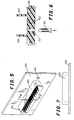
- FIGURE 1 is a perspective view of a female D-shell connector according to the present invention.
- FIGURE 2 shows a bottom view of the female D-shell connector of FIGURE 1.
- FIGURE 3 shows a side view of the female D-shell connector of FIGURE 1.
- FIGURE 4 is a sectional view of the female D-shell connector of FIGURE 1 taken along lines A-A.
- FIGURE 5 is a perspective view of a male D-shell connector according to the present invention.
- FIGURE 6 is a side view of the male D-shell connector shown in FIGURE 5 without the pins or pin holes.
- FIGURE 7 is a sectional view of the male D-shell connector of FIGURE 5 taken along lines B-B.
- a planar substrate 10 is molded as an integral portion of the connector and may be for example a printed wiring board (PWB).
- the substrate includes an approximately D-shaped block 14 extending from a surface thereof.
- the outer side surfaces 16 of the block 14 may be plated with a conductive material by a process such as that disclosed in the above application to Mettler et al or other appropriate process.
- This D-shaped block 14 will have essentially the dimensions of one of the many variations of a standard female D-shell connector.
- the block 14 includes a top surface 18 which is essentially free of conductive plating.
- Top surface 18 carries a plurality of plated through holes such as 22 extending from this top surface 18 to the bottom of the substrate.
- 25 such plated through holes are shown, but this is not to be limiting since many standard and non-standard conductor numbers are possible.
- the plated through holes 22 of the present invention are connected to plated conductors 26 on the lower surface of the printed wiring board substrate 10 as shown in FIGURE 2. These plated through holes 22 may thus be connected to electrical circuit components disposed on the circuit board as required or may be attached to wires via these conductors in a conventional manner.
- D-shell connectors When D-shell connectors are mated together, they are frequently secured into place by a screw connection. To permit such connection, frequently stand-offs are placed between the connectors to facilitate a good mechanical fit which will not place undue stresses on the mating pins.
- a pair of integral stand-offs 30 having a screw hole 32 passing therethrough may be provided as an integral molded part of the substrate 10.
- FIGURE 3 A side view of the connector of FIGURE 1 is shown in FIGURE 3.
- the junction of the sides 16 with the upper surface 18 may be chamfered at 45°.
- the through holes 22 may have a funnel shape at the top.
- the topmost portion of the through hole 22 is square in cross section and is formed that way in the molding process.
- the remainder of the through holes 22 are also square in cross section but may be round to more closely conform with the shape of the mating pin of the male connector. This shape is of course not to be limiting since a round or oval cross section hole or other shape could also be used.
- Holes 22 may be tapered slightly from top to bottom so that the springs are gradually loaded as a male connector is inserted. In the preferred embodiment, this taper is from about 0.032 to about 0.026 inches
- the contact forces between the male pin and the female plastic spring are set by the tolerances between the two mating parts through the range of tolerances.
- the contact forces are designed to provide between approximately 150 and 500 grams of normal force. Tighter tolerances may be used to narrow this range if desired.
- the design preferrably limits the displacement of the plastic material to a degree which prevents the plastic material from experiencing significant stress.
- a channel 38 is molded or cut between the two rows of apertures 22 to provide relief in the plastic substrate to permit it to flex somewhat when pins are inserted into the through holes 22.
- This relief channel 38 allows the plastic walls of the through holes 22 to flex and act as springs to tightly compress the mating pins of the male connector.
- the two rows of through holes 22 are separated by approximately 0.112 inch. Adjacent through holes 22 in the rows are separated by approximately 0.109 inch and opposing holes in each row are staggered.
- the relief channel 38 is approximately 0.036 inch wide and approximately 0.178 inch deep.
- the preferred material for use in making the substrate is General Electric Ultem 2312. Of course, these materials and measurements are not intended to be limiting, but rather illustrative. Other materials and dimensions may prove suitable.
- the outside layer of metalization within the female connector may be copper, nickel, gold or a variety of other materials.
- the outside surface of the connector may be plated with a variety of materials also but is preferrably plated with nickel to provide a durable, abrasion resistant surface.
- a planar substrate 50 which may be a printed wiring board includes a plurality of plated through holes 52 which are fitted with commercially available or custom made metal pins 56. Such pins 56 are installed as a secondary operation by press fitting the pins 56 into the plated through holes 52 in a known manner.
- Through holes 52 preferrably include a wider tapered area adjacent the lower surface of the substrate and a narrower portion near the upper surface of the substrate. This forms a compliant contact surface for the pin 56 reducing or eliminating the need for the pin 56 to be soldered into place.
- These through holes 52 are arranged in two staggered rows to match the mating female connector as shown in FIGURE 1.
- the two rows of through holes are surrounded by a D-shaped wall 60 which is suitably dimensioned to mate outside the D-shaped block of the mating female connector.
- the inner and / or the outer surfaces of the D-shaped wall 60 may be plated with a shield conductor if desired according to the process described in the above John Mettler et al. application.
- the bottom and / or top surface of the substrate 50 may be plated in a manner similar to that of substrate 10 to form a part of a printed wiring board.
- the plated through holes 52 are electrically connected to plated conductors on the lower surface of the substrate 50 to make appropriate electrical contact with the pins 56.
- the substrate 50 may be provided with screw holes 64 which align with screw holes 32 of stand offs 30 in the female connector.
Landscapes
- Engineering & Computer Science (AREA)
- Microelectronics & Electronic Packaging (AREA)
- Coupling Device And Connection With Printed Circuit (AREA)
Priority Applications (1)
| Application Number | Priority Date | Filing Date | Title |
|---|---|---|---|
| EP92306454A EP0578880A1 (de) | 1992-07-14 | 1992-07-14 | Metallisierter D-Verbinder mit Umhüllung |
Applications Claiming Priority (1)
| Application Number | Priority Date | Filing Date | Title |
|---|---|---|---|
| EP92306454A EP0578880A1 (de) | 1992-07-14 | 1992-07-14 | Metallisierter D-Verbinder mit Umhüllung |
Publications (1)
| Publication Number | Publication Date |
|---|---|
| EP0578880A1 true EP0578880A1 (de) | 1994-01-19 |
Family
ID=8211432
Family Applications (1)
| Application Number | Title | Priority Date | Filing Date |
|---|---|---|---|
| EP92306454A Withdrawn EP0578880A1 (de) | 1992-07-14 | 1992-07-14 | Metallisierter D-Verbinder mit Umhüllung |
Country Status (1)
| Country | Link |
|---|---|
| EP (1) | EP0578880A1 (de) |
Cited By (4)
| Publication number | Priority date | Publication date | Assignee | Title |
|---|---|---|---|---|
| GB2289170A (en) * | 1994-05-06 | 1995-11-08 | Sony Corp | Printed circuit board solder thief |
| GB2289169A (en) * | 1994-04-06 | 1995-11-08 | Harper Jones Francis David | Printed circuit key for vehicle security |
| EP0836757A4 (de) * | 1995-06-12 | 1999-11-03 | Berg Tech Inc | Elektrischer verbinder und elektrische kabelanordnung mit niedrigem übersprechen und gesteuertem impedanzverhalten |
| CN114619273A (zh) * | 2022-03-31 | 2022-06-14 | 西安航空制动科技有限公司 | 一种壳体零件二维及三维孔系的加工装置及加工方法 |
Citations (5)
| Publication number | Priority date | Publication date | Assignee | Title |
|---|---|---|---|---|
| EP0189288A2 (de) * | 1985-01-18 | 1986-07-30 | E.I. Du Pont De Nemours And Company | Abgeschirmte Verbindungsleiste und Zusammenbau |
| US4708412A (en) * | 1986-05-20 | 1987-11-24 | Amp Incorporated | Electrical connector having low inductance shield |
| US4921453A (en) * | 1989-04-13 | 1990-05-01 | Ici Americas Inc. | Molded complaint springs |
| US4969842A (en) * | 1989-11-30 | 1990-11-13 | Amp Incorporated | Molded electrical connector having integral spring contact beams |
| US5127838A (en) * | 1990-02-23 | 1992-07-07 | General Electric Company | Plated electrical connectors |
-
1992
- 1992-07-14 EP EP92306454A patent/EP0578880A1/de not_active Withdrawn
Patent Citations (5)
| Publication number | Priority date | Publication date | Assignee | Title |
|---|---|---|---|---|
| EP0189288A2 (de) * | 1985-01-18 | 1986-07-30 | E.I. Du Pont De Nemours And Company | Abgeschirmte Verbindungsleiste und Zusammenbau |
| US4708412A (en) * | 1986-05-20 | 1987-11-24 | Amp Incorporated | Electrical connector having low inductance shield |
| US4921453A (en) * | 1989-04-13 | 1990-05-01 | Ici Americas Inc. | Molded complaint springs |
| US4969842A (en) * | 1989-11-30 | 1990-11-13 | Amp Incorporated | Molded electrical connector having integral spring contact beams |
| US5127838A (en) * | 1990-02-23 | 1992-07-07 | General Electric Company | Plated electrical connectors |
Cited By (8)
| Publication number | Priority date | Publication date | Assignee | Title |
|---|---|---|---|---|
| GB2289169A (en) * | 1994-04-06 | 1995-11-08 | Harper Jones Francis David | Printed circuit key for vehicle security |
| GB2289169B (en) * | 1994-04-06 | 1998-05-06 | Harper Jones Francis David | Security coupling |
| GB2289170A (en) * | 1994-05-06 | 1995-11-08 | Sony Corp | Printed circuit board solder thief |
| GB2289170B (en) * | 1994-05-06 | 1998-06-24 | Sony Corp | Circuit board |
| EP0836757A4 (de) * | 1995-06-12 | 1999-11-03 | Berg Tech Inc | Elektrischer verbinder und elektrische kabelanordnung mit niedrigem übersprechen und gesteuertem impedanzverhalten |
| EP1594184A3 (de) * | 1995-06-12 | 2005-12-14 | Fci | Elektrischer Verbinder und elektrische Kabelanordnung mit niedrigem Übersprechen und gesteuertem Impedanzverhalten |
| CN114619273A (zh) * | 2022-03-31 | 2022-06-14 | 西安航空制动科技有限公司 | 一种壳体零件二维及三维孔系的加工装置及加工方法 |
| CN114619273B (zh) * | 2022-03-31 | 2023-08-04 | 西安航空制动科技有限公司 | 一种壳体零件二维及三维孔系的加工装置及加工方法 |
Similar Documents
| Publication | Publication Date | Title |
|---|---|---|
| US6652318B1 (en) | Cross-talk canceling technique for high speed electrical connectors | |
| EP0563942B1 (de) | Abgeschirmter elektrischer Verbinder | |
| JP3534478B2 (ja) | 電気コネクタ | |
| EP1274151B1 (de) | USB elektrischer Verbinder | |
| EP1032087B1 (de) | Verbindungsdose, verbindungsstecker und verbindungszusammenbau | |
| US6527592B2 (en) | Matching male and female connector assembly | |
| US6705902B1 (en) | Connector assembly having contacts with uniform electrical property of resistance | |
| US4457570A (en) | Connector for mating modular plug with printed circuit board | |
| US5102353A (en) | Electrical connectors | |
| US7044748B2 (en) | Electrical device for interconnecting two printed circuit boards at a large distance | |
| EP0657960B1 (de) | Leiterplattenverbinder | |
| US3569900A (en) | Electrical connector assembly | |
| EP0073957A2 (de) | Abgeschirmter elektrischer Verbinder | |
| US20090163078A1 (en) | Connector apparatus | |
| US5842887A (en) | Connector with improved shielding | |
| CA2211989C (en) | Connector having improved noise-shielding structure | |
| JP2005531121A (ja) | モジュール構造を有するインピーダンス調整された高密度コネクタ | |
| KR20020020783A (ko) | 임피던스가 조정되는 커넥터 | |
| US4869676A (en) | Connector assembly for use between mother and daughter circuit boards | |
| US6561821B1 (en) | High profile board-to-board electrical connector assembly | |
| WO2007002268A1 (en) | Electrical interconnection system | |
| US5127838A (en) | Plated electrical connectors | |
| US5158465A (en) | Audio jack connector | |
| EP1014513A2 (de) | Leiterplatte für Modularstecker | |
| EP0677215A4 (de) | Ein verbinder mit verbesserter abschirmung. |
Legal Events
| Date | Code | Title | Description |
|---|---|---|---|
| PUAI | Public reference made under article 153(3) epc to a published international application that has entered the european phase |
Free format text: ORIGINAL CODE: 0009012 |
|
| AK | Designated contracting states |
Kind code of ref document: A1 Designated state(s): BE DE ES FR GB IT NL SE |
|
| 17P | Request for examination filed |
Effective date: 19940630 |
|
| STAA | Information on the status of an ep patent application or granted ep patent |
Free format text: STATUS: THE APPLICATION HAS BEEN WITHDRAWN |
|
| 18W | Application withdrawn |
Withdrawal date: 19950830 |