EP0578899B1 - Verfahren zum Messen des Grades der Planheit einer dielektrischen Schicht in einer integrierten Schaltung und integrierter Schaltung mit einer Anordnung zur Durchführung dieses Verfahrens - Google Patents
Verfahren zum Messen des Grades der Planheit einer dielektrischen Schicht in einer integrierten Schaltung und integrierter Schaltung mit einer Anordnung zur Durchführung dieses Verfahrens Download PDFInfo
- Publication number
- EP0578899B1 EP0578899B1 EP92830382A EP92830382A EP0578899B1 EP 0578899 B1 EP0578899 B1 EP 0578899B1 EP 92830382 A EP92830382 A EP 92830382A EP 92830382 A EP92830382 A EP 92830382A EP 0578899 B1 EP0578899 B1 EP 0578899B1
- Authority
- EP
- European Patent Office
- Prior art keywords
- integrated circuit
- path
- measure
- dielectric layer
- planarity
- Prior art date
- Legal status (The legal status is an assumption and is not a legal conclusion. Google has not performed a legal analysis and makes no representation as to the accuracy of the status listed.)
- Expired - Lifetime
Links
Images

Classifications
-
- G—PHYSICS
- G01—MEASURING; TESTING
- G01B—MEASURING LENGTH, THICKNESS OR SIMILAR LINEAR DIMENSIONS; MEASURING ANGLES; MEASURING AREAS; MEASURING IRREGULARITIES OF SURFACES OR CONTOURS
- G01B21/00—Measuring arrangements or details thereof, where the measuring technique is not covered by the other groups of this subclass, unspecified or not relevant
- G01B21/30—Measuring arrangements or details thereof, where the measuring technique is not covered by the other groups of this subclass, unspecified or not relevant for measuring roughness or irregularity of surfaces
-
- G—PHYSICS
- G01—MEASURING; TESTING
- G01B—MEASURING LENGTH, THICKNESS OR SIMILAR LINEAR DIMENSIONS; MEASURING ANGLES; MEASURING AREAS; MEASURING IRREGULARITIES OF SURFACES OR CONTOURS
- G01B7/00—Measuring arrangements characterised by the use of electric or magnetic techniques
- G01B7/34—Measuring arrangements characterised by the use of electric or magnetic techniques for measuring roughness or irregularity of surfaces
- G01B7/345—Measuring arrangements characterised by the use of electric or magnetic techniques for measuring roughness or irregularity of surfaces for measuring evenness
Definitions
- This invention relates, in a first aspect thereof, to a process of measuring the degree of planarity of a dielectric layer in an integrated circuit, and in a second aspect, to an integrated circuit including means for performing the process.
- a variously shaped intermediate layer of polycrystalline silicon is first deposited onto a semiconductor substrate and then covered with a dielectric layer, both depositions being carried out using conventional photolithographic techniques. Due to the intermediate layer being discontinuous, the dielectric layer overlay usually exhibits a surface which is not perfectly than truly planar.
- the planarity of the dielectric layers has attained outstanding importance vis-a-vis the lithographic definition of the structures to be subsequently formed.
- the technique which is more generally employed to measure the degree of planarity is based on observation under the electron scan microscope of a section of the surface; thus, it becomes necessary to have the integrated circuit cut and destroyed. Consequently, this known technique can only be applied on a sampling basis and provides, in practice, a way of monitoring only the average quality of a production.
- a laser interferometer technology in which the distance between a reference surface and the surface of the substrate is related to the number of interference bands of a laser beam.
- an electrical capacitance technology is disclosed, in which flatness is determined by comparing an internal capacitance to the capacitance established between the tip of an electrical probe and the nearby substrate surface.
- an air gauging technology is disclosed, in which flatness is determined by measuring the volume of pressurized gas (nitrogen) allowed to escape between a precision nozzle and the nearby surface of the substrate.
- pressurized gas nitrogen
- GB-A-2083229 discloses a flatness measuring apparatus making use of a number of detecting probes, each of them being of the types mentioned above.
- the problem addressed by this invention is that of providing a non-destructive process whereby the degree of planarity of a dielectric layer in an integrated circuit can be measured.
- this invention provides, in a first aspect thereof, a process of measuring the degree of planarity of a dielectric layer in an integrated circuit, being characterized in that it comprises the steps of: depositing, onto a dielectric layer to be measured for planarity, a predetermined measure path of a conductive film; depositing a reference path identical with the measure path over a perfectly planar surface; and measuring the electric resistance through said measurement path against the electric resistance of the reference path.
- the resistance of the measure path is minimal where the deposition surface is perfectly planar, and increases as the surface deviates from perfect planarity.
- the measure path resistance is measured against the resistance of a reference path identical with the measure path but deposited across a perfectly planar surface, so that the resistance value is not affected by errors; moreover, a comparative process is definitely more convenient.
- the measure and reference paths are formed on the same integrated circuit, the former onto the portion to be tested for planarity and the latter onto perfecty planar portions.
- both the measure path and the reference paths can be formed jointly under the same conditions and on the same equipment, to thereby minimize the likelihood of resistance differentials arising from structural differences in the paths which are unrelated to the degree of planarity.
- a second aspect of the invention provides an integrated circuit comprising a continuous semiconductor substrate, a discontinuous intermediate layer (typically of polycrystalline silicon) disposed over a portion of the substrate, a dielectric layer deposited onto the substrate and the discontinuous intermediate layer, said dielectric layer having a surface to be tested for planarity, characterized in that it is provided with a measure path of a conductive film deposited across said surface of the dielectric layer at the location of the portion with the discontinuous intermediate layer and a reference path of a conductive film being identical with the measure path and deposited onto a perfectly planar portion of the integrated circuit.
- Such an integrated circuit includes the barely necessary for performing the aforesaid process.
- the circuit includes said measure path and three such reference paths so interlinked electrically as to form a Wheatstone bridge arrangement.
- the three reference paths are formed on peripheral portions of the integrated circuit.
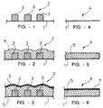
- a continuous semiconductor substrate of an integrated circuit In a portion 2 of the integrated circuit, a discontinuous intermediate layer 3, e.g. of polycrystalline silicon, is deposited over the substrate 1.
- a discontinuous intermediate layer e.g. of polycrystalline silicon
- the substrate 1 has no discontinuous intermediate overlay, and the portions 4 are, therefore, perfectly planar.
- a dielectric covering layer 5 is added.
- the surface of the dielectric layer 5 is not perfectly planar, and shows undulations which follow the run of the underlying layer 3; in the portions 4, the surface of the dielectric layer 5 is instead perfectly planar because perfectly planar is the surface on which it is deposited.
- a metallic conductive film is deposited over the dielectric layer 5 into a measure path 6 and three reference paths 7, as shown in Figures 3, 6 and 7.
- the four paths are all identical with one another (in plan view, as previously explained) and laid into a preferably meandering pattern so as to concentrate the longest possible path within the smallest possible area.
- the measure path 6 is deposited at the portion 2 of the integrated circuit, whilst the reference paths 7 are deposited at the portions 4 thereof. As for the measure path 6, it is laid such that its individual straight sections are oriented substantially perpendicular to any substantially straight sections of the discontinuous intermediate layer 3.
- the electric resistance of the path will show a given value; on the other hand, where the surface is not planar, then the electric resistance of the path will be the higher, the greater is the deviation of the surface from perfect planarity.
- the resistance R M of the measure path 6 is higher than the resistance R C of the reference path 7, and the degree of planarity of the surface can be appreciated from the value of the resistance R M .
- the measure path 6 three reference paths 7, connecting sections 9, and terminals 10 are all disposed into a Wheatstone bridge arrangement.
- the resistive value thus obtained is then checked against a preset scale indicating the degree of planarity.
- This scale can be established empirically.
- this measuring process of the degree of planarity can be readily incorporated to the standard sequence of electric tests which any integrated circuit is to go through.
Landscapes
- Physics & Mathematics (AREA)
- General Physics & Mathematics (AREA)
- Testing Or Measuring Of Semiconductors Or The Like (AREA)
- Measurement Of Length, Angles, Or The Like Using Electric Or Magnetic Means (AREA)
Claims (7)
- Verfahren zum Messen des Planheitsgrades einer dielektrischen Schicht (5) in einer integrierten Schaltung (1), gekennzeichnet durch die folgenden Verfahrensschritte:- Aufbringen eines vorgegebenen Meßweges (6) aus einem leitenden Film auf eine dielektrische Schicht (5), deren Planheit gemessen werden soll;- Aufbringen eines Bezugsweges (7), der identisch zu dem Meßweg (6) ist, auf eine vollkommen ebene Oberfläche (4); und- Messen des elektrischen Widerstandes durch den Meßweg (6) im Vergleich zu dem elektrischen Widerstand des Bezugsweges (7).
- Verfahren nach Anspruch 1, bei dem die Vergleichsmessung mit einer Wheatstone-Brückenanordnung durchgeführt wird, welche einen Meßweg (6) und drei identische Bezugswege (7) aufweist.
- Verfahren nach Anspruch 2, bei dem die Meß- und Bezugswege (6, 7) in derselben integrierten Schaltung (1) ausgebildet werden, ersterer auf dem Teil (2) der Schaltung, dessen Planheit gemessen werden soll, und letzterer auf vollkommen ebenen Teilen (4).
- Verfahren nach Anspruch 3, bei dem die vollkommen ebenen Teile mit den Bezugswegen (7) darauf Randabschnitte (4) der integrierten Schaltung (1) sind.
- Integrierte Schaltung mit einem zusammenhängenden Substrat (1), einer unterbrochenen Zwischenschicht (3), die über einem Teil (2) des Substrats (1) angeordnet ist, einer dielektrischen Schicht (5), die auf dem Substrat (1) und der unterbrochenen Zwischenschicht (3) liegt, wobei die dielekrische Schicht (5) eine Oberfläche aufweist, deren Planheit geprüft werden soll, dadurch gekennzeichnet, daß sie einen Meßweg (6) aus einem leitenden Film aufweist, der über der Oberfläche der dielektrischen Schicht (5) bei dem Ort des Teiles (2) mit der unterbrochenen Schicht (3) liegt, und einen Bezugsweg (7) aus einem leitendem Film aufweist, der identisch zu dem Meßweg (6) ist und auf einem vollkommen ebenen Teil (4) der integrierten Schaltung (1) liegt.
- Integrierte Schaltung nach Anspruch 5, welche den Meßweg (6) und drei derartige Bezugswege (7) umfaßt, die elektrisch in einer Wheatstone-Brückenanordnung miteinander verbunden sind.
- Integrierte Schaltung nach Anspruch 6, bei der die drei Bezugswege (6) auf Randabschnitten (4) der integrierten Schaltung (1) ausgebildet sind.
Priority Applications (4)
| Application Number | Priority Date | Filing Date | Title |
|---|---|---|---|
| DE69216223T DE69216223T2 (de) | 1992-07-15 | 1992-07-15 | Verfahren zum Messen des Grades der Planheit einer dielektrischen Schicht in einer integrierten Schaltung und integrierter Schaltung mit einer Anordnung zur Durchführung dieses Verfahrens |
| EP92830382A EP0578899B1 (de) | 1992-07-15 | 1992-07-15 | Verfahren zum Messen des Grades der Planheit einer dielektrischen Schicht in einer integrierten Schaltung und integrierter Schaltung mit einer Anordnung zur Durchführung dieses Verfahrens |
| US08/092,717 US5543633A (en) | 1992-07-15 | 1993-07-15 | Process and structure for measuring the planarity degree of a dielectric layer in an integrated circuit and integrated circuit including means for performing said process |
| JP5175575A JPH0714904A (ja) | 1992-07-15 | 1993-07-15 | 集積回路における誘電層の平坦性測定方法及び回路 |
Applications Claiming Priority (1)
| Application Number | Priority Date | Filing Date | Title |
|---|---|---|---|
| EP92830382A EP0578899B1 (de) | 1992-07-15 | 1992-07-15 | Verfahren zum Messen des Grades der Planheit einer dielektrischen Schicht in einer integrierten Schaltung und integrierter Schaltung mit einer Anordnung zur Durchführung dieses Verfahrens |
Publications (2)
| Publication Number | Publication Date |
|---|---|
| EP0578899A1 EP0578899A1 (de) | 1994-01-19 |
| EP0578899B1 true EP0578899B1 (de) | 1996-12-27 |
Family
ID=8212139
Family Applications (1)
| Application Number | Title | Priority Date | Filing Date |
|---|---|---|---|
| EP92830382A Expired - Lifetime EP0578899B1 (de) | 1992-07-15 | 1992-07-15 | Verfahren zum Messen des Grades der Planheit einer dielektrischen Schicht in einer integrierten Schaltung und integrierter Schaltung mit einer Anordnung zur Durchführung dieses Verfahrens |
Country Status (4)
| Country | Link |
|---|---|
| US (1) | US5543633A (de) |
| EP (1) | EP0578899B1 (de) |
| JP (1) | JPH0714904A (de) |
| DE (1) | DE69216223T2 (de) |
Families Citing this family (13)
| Publication number | Priority date | Publication date | Assignee | Title |
|---|---|---|---|---|
| JPH09107048A (ja) * | 1995-03-30 | 1997-04-22 | Mitsubishi Electric Corp | 半導体パッケージ |
| JPH09129695A (ja) * | 1995-10-30 | 1997-05-16 | Mitsubishi Electric Corp | 誘電体膜評価用テスト構造 |
| US6054720A (en) * | 1997-11-06 | 2000-04-25 | International Business Machines Corporation | Apparatus and method for evaluating the surface insulation resistance of electronic assembly manufacture |
| US5952674A (en) * | 1998-03-18 | 1999-09-14 | International Business Machines Corporation | Topography monitor |
| US6384466B1 (en) * | 1998-08-27 | 2002-05-07 | Micron Technology, Inc. | Multi-layer dielectric and method of forming same |
| US6684520B1 (en) | 2000-02-25 | 2004-02-03 | Xilinx, Inc. | Mask-alignment detection circuit in x and y directions |
| US6393714B1 (en) | 2000-02-25 | 2002-05-28 | Xilinx, Inc. | Resistor arrays for mask-alignment detection |
| US6305095B1 (en) * | 2000-02-25 | 2001-10-23 | Xilinx, Inc. | Methods and circuits for mask-alignment detection |
| US6563320B1 (en) * | 2000-02-25 | 2003-05-13 | Xilinx, Inc. | Mask alignment structure for IC layers |
| US6621280B1 (en) * | 2000-06-27 | 2003-09-16 | Agere Systems Inc. | Method of testing an integrated circuit |
| US7427857B2 (en) * | 2002-12-13 | 2008-09-23 | Nxp B.V. | Resistor structures to electrically measure unidirectional misalignment of stitched masks |
| CN101814453B (zh) * | 2010-04-08 | 2012-03-21 | 复旦大学 | 一种用于硅通孔互连中的硅片对准方法 |
| CN117146764B (zh) * | 2023-10-27 | 2024-01-05 | 江苏优创红外科技有限公司 | 一种光学镜片表面平整度检测设备 |
Family Cites Families (7)
| Publication number | Priority date | Publication date | Assignee | Title |
|---|---|---|---|---|
| US3974443A (en) * | 1975-01-02 | 1976-08-10 | International Business Machines Corporation | Conductive line width and resistivity measuring system |
| US4331035A (en) * | 1979-11-13 | 1982-05-25 | Gould Inc. | Geometric balance adjustment of thin film strain gage sensors |
| JPS5744807A (en) * | 1980-08-29 | 1982-03-13 | Hitachi Ltd | Flatness measuring apparatus |
| US4918377A (en) * | 1988-12-05 | 1990-04-17 | The United States Of America As Represented By The Administrator Of The National Aeronautics And Space Administration | Integrated circuit reliability testing |
| US5081421A (en) * | 1990-05-01 | 1992-01-14 | At&T Bell Laboratories | In situ monitoring technique and apparatus for chemical/mechanical planarization endpoint detection |
| DE69034137D1 (de) * | 1990-10-01 | 2004-06-03 | St Microelectronics Srl | Herstellung von Kontaktanschlüssen bei der alles überdeckenden CVD-Abscheidung und Rückätzen |
| JPH04261023A (ja) * | 1991-01-21 | 1992-09-17 | Mitsubishi Electric Corp | 半導体装置 |
-
1992
- 1992-07-15 EP EP92830382A patent/EP0578899B1/de not_active Expired - Lifetime
- 1992-07-15 DE DE69216223T patent/DE69216223T2/de not_active Expired - Fee Related
-
1993
- 1993-07-15 JP JP5175575A patent/JPH0714904A/ja active Pending
- 1993-07-15 US US08/092,717 patent/US5543633A/en not_active Expired - Lifetime
Also Published As
| Publication number | Publication date |
|---|---|
| EP0578899A1 (de) | 1994-01-19 |
| DE69216223T2 (de) | 1997-07-10 |
| US5543633A (en) | 1996-08-06 |
| JPH0714904A (ja) | 1995-01-17 |
| DE69216223D1 (de) | 1997-02-06 |
Similar Documents
| Publication | Publication Date | Title |
|---|---|---|
| EP0578899B1 (de) | Verfahren zum Messen des Grades der Planheit einer dielektrischen Schicht in einer integrierten Schaltung und integrierter Schaltung mit einer Anordnung zur Durchführung dieses Verfahrens | |
| US5528153A (en) | Method for non-destructive, non-contact measurement of dielectric constant of thin films | |
| US4516071A (en) | Split-cross-bridge resistor for testing for proper fabrication of integrated circuits | |
| US4918377A (en) | Integrated circuit reliability testing | |
| US5982166A (en) | Method for measuring a characteristic of a semiconductor wafer using cylindrical control | |
| EP0253460B1 (de) | Verfahren und Vorrichtung zum Festlegen der Spalttiefe von in Mengen angefertigten magnetischen Dünnfilm-Wandlern | |
| US5712571A (en) | Apparatus and method for detecting defects arising as a result of integrated circuit processing | |
| US5898478A (en) | Method of using a test reticle to optimize alignment of integrated circuit process layers | |
| EP1286389B1 (de) | Verfahren und Vorrichtung zum Testen von Halbleiterwafern | |
| US3808527A (en) | Alignment determining system | |
| US5876264A (en) | Deposition process windage calibration | |
| US5329334A (en) | Integrated circuit test reticle and alignment mark optimization method | |
| US4437760A (en) | Reusable electrical overlay measurement circuit and process | |
| US4782288A (en) | Method for evaluating processing parameters in the manufacture of semiconductor devices | |
| KR101252885B1 (ko) | 기판 상의 도전층에 대한 전기 응답을 최적화하기 위한방법 및 장치 | |
| US3609537A (en) | Resistance standard | |
| GB2326721A (en) | Wire width measurement | |
| US7550303B2 (en) | Systems and methods for overlay shift determination | |
| EP0602606B1 (de) | Herstellungsverfahren für Dehnungswandler | |
| US20030210058A1 (en) | Electrical print resolution test die | |
| CN112820715A (zh) | 校准用晶圆级在片电阻标准样片及制备方法 | |
| KR101303970B1 (ko) | 기판 상의 일 세트의 도전층에 대한 전기 응답을최적화하기 위한 방법 및 장치 | |
| US20040070393A1 (en) | Differential measurement method using eddy-current sensing to resolve a stack of conducting films on substrates | |
| CN118444023A (zh) | 一种航发钛合金叶片材料电阻率的精确测量方法 | |
| US4990218A (en) | Method of testing conductor film quality |
Legal Events
| Date | Code | Title | Description |
|---|---|---|---|
| PUAI | Public reference made under article 153(3) epc to a published international application that has entered the european phase |
Free format text: ORIGINAL CODE: 0009012 |
|
| AK | Designated contracting states |
Kind code of ref document: A1 Designated state(s): DE FR GB IT |
|
| 17P | Request for examination filed |
Effective date: 19940712 |
|
| 17Q | First examination report despatched |
Effective date: 19951016 |
|
| GRAG | Despatch of communication of intention to grant |
Free format text: ORIGINAL CODE: EPIDOS AGRA |
|
| GRAH | Despatch of communication of intention to grant a patent |
Free format text: ORIGINAL CODE: EPIDOS IGRA |
|
| GRAH | Despatch of communication of intention to grant a patent |
Free format text: ORIGINAL CODE: EPIDOS IGRA |
|
| GRAA | (expected) grant |
Free format text: ORIGINAL CODE: 0009210 |
|
| ITF | It: translation for a ep patent filed | ||
| AK | Designated contracting states |
Kind code of ref document: B1 Designated state(s): DE FR GB IT |
|
| REF | Corresponds to: |
Ref document number: 69216223 Country of ref document: DE Date of ref document: 19970206 |
|
| ET | Fr: translation filed |
Free format text: CORRECTIONS |
|
| PLBE | No opposition filed within time limit |
Free format text: ORIGINAL CODE: 0009261 |
|
| 26N | No opposition filed | ||
| REG | Reference to a national code |
Ref country code: GB Ref legal event code: IF02 |
|
| PGFP | Annual fee paid to national office [announced via postgrant information from national office to epo] |
Ref country code: DE Payment date: 20020724 Year of fee payment: 11 |
|
| PG25 | Lapsed in a contracting state [announced via postgrant information from national office to epo] |
Ref country code: DE Free format text: LAPSE BECAUSE OF NON-PAYMENT OF DUE FEES Effective date: 20040203 |
|
| PGFP | Annual fee paid to national office [announced via postgrant information from national office to epo] |
Ref country code: FR Payment date: 20040708 Year of fee payment: 13 |
|
| PGFP | Annual fee paid to national office [announced via postgrant information from national office to epo] |
Ref country code: GB Payment date: 20040714 Year of fee payment: 13 |
|
| PG25 | Lapsed in a contracting state [announced via postgrant information from national office to epo] |
Ref country code: IT Free format text: LAPSE BECAUSE OF NON-PAYMENT OF DUE FEES;WARNING: LAPSES OF ITALIAN PATENTS WITH EFFECTIVE DATE BEFORE 2007 MAY HAVE OCCURRED AT ANY TIME BEFORE 2007. THE CORRECT EFFECTIVE DATE MAY BE DIFFERENT FROM THE ONE RECORDED. Effective date: 20050715 Ref country code: GB Free format text: LAPSE BECAUSE OF NON-PAYMENT OF DUE FEES Effective date: 20050715 |
|
| GBPC | Gb: european patent ceased through non-payment of renewal fee |
Effective date: 20050715 |
|
| PG25 | Lapsed in a contracting state [announced via postgrant information from national office to epo] |
Ref country code: FR Free format text: LAPSE BECAUSE OF NON-PAYMENT OF DUE FEES Effective date: 20060331 |
|
| REG | Reference to a national code |
Ref country code: FR Ref legal event code: ST Effective date: 20060331 |