EP0580199A1 - Détecteur Viterbi adaptatif - Google Patents
Détecteur Viterbi adaptatif Download PDFInfo
- Publication number
- EP0580199A1 EP0580199A1 EP93201868A EP93201868A EP0580199A1 EP 0580199 A1 EP0580199 A1 EP 0580199A1 EP 93201868 A EP93201868 A EP 93201868A EP 93201868 A EP93201868 A EP 93201868A EP 0580199 A1 EP0580199 A1 EP 0580199A1
- Authority
- EP
- European Patent Office
- Prior art keywords
- signal
- detection signal
- input
- difference metric
- deriving
- Prior art date
- Legal status (The legal status is an assumption and is not a legal conclusion. Google has not performed a legal analysis and makes no representation as to the accuracy of the status listed.)
- Granted
Links
- 230000003044 adaptive effect Effects 0.000 title description 3
- 238000012937 correction Methods 0.000 claims abstract description 36
- 238000001514 detection method Methods 0.000 claims description 65
- 230000005540 biological transmission Effects 0.000 claims description 22
- 230000006870 function Effects 0.000 abstract description 59
- 230000004044 response Effects 0.000 description 6
- 238000012546 transfer Methods 0.000 description 5
- 230000006978 adaptation Effects 0.000 description 4
- 230000009977 dual effect Effects 0.000 description 2
- 230000000694 effects Effects 0.000 description 2
- 238000006467 substitution reaction Methods 0.000 description 2
- 230000007704 transition Effects 0.000 description 2
- 230000003111 delayed effect Effects 0.000 description 1
- 238000009795 derivation Methods 0.000 description 1
- 230000008030 elimination Effects 0.000 description 1
- 238000003379 elimination reaction Methods 0.000 description 1
- 238000005516 engineering process Methods 0.000 description 1
- 238000011156 evaluation Methods 0.000 description 1
- 230000002045 lasting effect Effects 0.000 description 1
- 238000000034 method Methods 0.000 description 1
- 230000003287 optical effect Effects 0.000 description 1
- 238000011160 research Methods 0.000 description 1
- 238000010079 rubber tapping Methods 0.000 description 1
- 238000001228 spectrum Methods 0.000 description 1
- 239000002023 wood Substances 0.000 description 1
Images


Classifications
-
- H—ELECTRICITY
- H03—ELECTRONIC CIRCUITRY
- H03M—CODING; DECODING; CODE CONVERSION IN GENERAL
- H03M13/00—Coding, decoding or code conversion, for error detection or error correction; Coding theory basic assumptions; Coding bounds; Error probability evaluation methods; Channel models; Simulation or testing of codes
- H03M13/65—Purpose and implementation aspects
- H03M13/6502—Reduction of hardware complexity or efficient processing
-
- H—ELECTRICITY
- H03—ELECTRONIC CIRCUITRY
- H03M—CODING; DECODING; CODE CONVERSION IN GENERAL
- H03M13/00—Coding, decoding or code conversion, for error detection or error correction; Coding theory basic assumptions; Coding bounds; Error probability evaluation methods; Channel models; Simulation or testing of codes
- H03M13/37—Decoding methods or techniques, not specific to the particular type of coding provided for in groups H03M13/03 - H03M13/35
- H03M13/39—Sequence estimation, i.e. using statistical methods for the reconstruction of the original codes
- H03M13/41—Sequence estimation, i.e. using statistical methods for the reconstruction of the original codes using the Viterbi algorithm or Viterbi processors
-
- H—ELECTRICITY
- H03—ELECTRONIC CIRCUITRY
- H03M—CODING; DECODING; CODE CONVERSION IN GENERAL
- H03M13/00—Coding, decoding or code conversion, for error detection or error correction; Coding theory basic assumptions; Coding bounds; Error probability evaluation methods; Channel models; Simulation or testing of codes
- H03M13/65—Purpose and implementation aspects
- H03M13/6502—Reduction of hardware complexity or efficient processing
- H03M13/6505—Memory efficient implementations
Definitions
- the invention relates to a transmission system comprising a data transmitter for supplying with a symbol interval data symbols to an input of a channel and a data receiver comprising a means for deriving a detection signal from an output signal of the channel, a means for deriving from the detection signal the most likely sequence of data symbols carried by the detection signal by recursively updating two candidate data sequences (survivors) on the basis of the value of a difference metric which is a measure for the probability difference of the survivors, the detection means furthermore including an adapting means for updating the difference metric, the new difference metric depending on a saturation function of the previous difference metric, and the saturation function for an ordinate value interval being dual to the identity function.
- the invention likewise relates to a receiver to be used in a system of this type.
- Transmission systems of this type may be used, for example, for transmitting data signals through the public telephone network or for reconstructing data signals from a magnetic tape or disc.
- the analog pulses do not overlap in time. If the medium has a limited bandwidth, the pulses will start overlapping which in many cases will lead to the fact that the value of the received detection signal not only depends on a single data symbol at a given instant, but also on data symbols neighbouring in time. This effect is termed intersymbol interference.
- Intersymbol interference may be caused not only by a limited bandwidth of the medium, but also by the use of a band limiting filter on the transmitter side which is used for giving a desired shape to the frequency spectrum of the transmitted or recorded analog pulses.
- the presence of intersymbol interference will often lead to an enhancement of the bit error rate.
- An optimum receiver which would (substantially) completely eliminate the influence of intersymbol interference, would determine any possible sequence of transmitted data symbols and would determine the associated detection signal which would have been received if the relevant sequence of data symbols had been transmitted through a noise-free channel. By comparing with the current detection signal all the detection signals thus obtained, the most likely sequence of transmitted data symbols could be determined. Such a receiver, however, would require an impracticably large computer and storage capacity.
- a commonly termed Viterbi detector is often used.
- each survivor when a next data symbol is received, is extended and split up into a plurality of survivors of which only the most recently appended data symbols are different.
- the probability measure belonging to each new survivor is derived from the probability measure of the survivor from which the new survivor is derived and from an even function belonging to this new survivor of the difference between the current detection signal and the expected detection signal. Suitable even functions are the commonly termed L1 norm (
- Viterbi detector In aforementioned journal article a further simplification of the Viterbi detector is proposed which is possible if no more than two survivors need to be updated. This is the case if the number of possible values L of the transmission signal or recording signal is equal to two, and if the transfer is equal to 1+D or 1-D, where D represents a one symbol interval delay of the channel input signal. Since in this situation no more than two survivors need to be updated, it may be sufficient in lieu of updating a probability measure for each survivor, to update no more than one difference metric which is a measure for the difference between the two survivors.
- the known Viterbi detector may also be used for channels having a transfer function of 1+D n or 1-D n .
- n such Viterbi detectors are to be used whilst samples of the detection signals are alternately applied to the various Viterbi detectors. This also results in the fact that the necessary operation rate of each Viterbi detector may be reduced by a factor of n.
- a new value of the difference metric belonging to a new value of the detection signal is equal to a saturation function of the difference between the old difference metric and a signal that is proportional to the detection signal.
- the saturation values are determined, for example, by the assumed properties of the channel and the norm (for example, L1 or L2) used for determining the difference metric.
- the new value of the difference metric there can be directly determined how the survivors are to be extended. If the new value of the difference metric is situated in the (substantially) linear interval of the saturation function, the two survivors are to be extended by a symbol that has a value equal to the value of the most recent symbol of this survivor. In the two saturation regions in which the new difference metric may be situated, the new survivors are obtained by extending the first or second survivor to two new survivors by adding thereto the two possible symbol values. There has been assumed in this context that no precoding of the symbols to be transmitted or recorded respectively, has occurred, because when precoding is used there is a possibility of combining the inverse precoding with survivor generation.
- a problem of the prior-art transmission system is that it presents only optimum performance with a limited class of channels having a very specific transfer function i.e. (1+D n ) or (1-D n ).
- the invention is characterized, in that the new difference metric is a combination of the saturation function and a correction signal, this correction signal depending on the detection signal and on a correction parameter which is a measure for a difference between a current channel parameter and an assumed channel parameter.
- An embodiment of the invention is characterized, in that the size of the ordinate value interval is proportional to an estimate of the amplitude of the detection signal.
- the size of the (substantially) linear region proportional to an estimate of the amplitude of the detection signal, there is obtained that the data receiver continues to operate well for detection signals which have different amplitudes.
- the use of, for example, an AGC amplifier for keeping the input signal of the detection means constant, may be omitted.
- a further embodiment of the invention is characterized, in that the detection means comprises a means for storing and adapting the difference metric in the form of at least two components and for updating the survivors on the basis of the value of the components.
- the difference metric By storing the difference metric in the form of at least two components there is achieved that a simpler storage means may suffice for this storage. Then it is not necessary that for each new value of the detection signal the difference metric is actually derived from the components. It is conceivable that the adaptation and evaluation of the difference metric may be effected on the basis of said components without the need of constantly determining the difference metric itself.
- a further embodiment of the invention is characterized, in that the means for deriving a detection signal from the input signal comprises a means for deriving a compensation signal for intersymbol interference from one of the survivors and a channel model stored in the detection means, and for deriving the detection signal by subtraction of the compensation signal from the input signal.
- the detection means By deriving the detection signal from the input signal and an intersymbol interference compensation signal derived from one of the survivors, it is possible to use the detection means for channels having an impulse response lasting longer than two symbol intervals of the detection signal, without a considerable enhancement of the complexity of the detection means.
- a preferred embodiment of the invention is characterized, in that the receiver comprises an adapting means for adaptively deriving the correction parameter from the detection signal.
- the receiver By adaptively deriving the value necessary for the correction parameter from the detection signal, the receiver is capable of automatically adapting itself to time-variable channels.
- Many methods are known for adaptively deriving channel parameters from a received input signal. A number of them are described in the title "Adaptive Digital Filters and Signal Analysis” by M.G. Bellanger, Marcel Dekker Inc., 1987, ISBN 0-8247-7788-0.
- a sequence of symbols a k to be transmitted is converted by a transmitter 2 into a signal suitable for transmission.
- This signal is fed to a channel 4.
- This channel may be a customary transmission channel, but also a magnetic or optical recording medium.
- the output signal of the channel 4 is applied to a receiver 6.
- a deriving means 8 for deriving a detection signal from an input signal derives a detection signal from the input signal of the receiver.
- the deriving means 8 habitually comprises a filter, for example, for partly suppressing intersymbol interference.
- the detection signal is applied to the detection means 10 which derives from the detection signal a decision â k of the sequence of transmitted symbols. It is likewise possible for the sequence of symbols â k to be applied to the deriving means 8 used for deriving the detection signal from the input signal.
- the detection means 10 as shown in Fig. 2 comprises a memory 14 for updating the difference metric ⁇ k .
- the adapting means here comprises an adder circuit 12 and a function generator 18 for generating the saturation function.
- the output of the memory 14 is connected to a first input of the function generator 18.
- the detection signal r k is applied to a second input of the function generator 18.
- An output of the function generator 18 carrying output signal S( ⁇ ) is connected to a first input of an adder circuit 12.
- a second input of the adder circuit 12 is supplied with a correction signal C k .
- the output of the adder circuit 12 is connected to an input of the memory 14.
- a second output of the function generator 18 carrying an output signal m+ is connected to a first input of an OR-gate 24 and to a control input LP of a shift register 20.
- a third output of the function generator 18 carrying output signal m ⁇ is connected to a first input of a OR-gate 26 and to a control input LP of a shift register 22.
- a fourth output of the function generator 18 carrying output signal m0 is connected to a second input of the OR-gate 24 ad to a second input of the OR-gate 26.
- the output of the OR-gate 24 is connected to a control input SH of the shift register 22.
- the output of the OR-gate 26 is connected to a control input SH of the shift register 20.
- a fixed logic “+1" value is applied to the input of the shift register 22 and a fixed logic “-1" value is applied to the input of the shift register 20.
- the output of each cell of the shift register 20 is coupled to a input of a successive cell of the shift register 22, whereas the output of each cell of the shift register 22 is coupled to a input of a successive cell of the shift register 20.
- the difference metric ⁇ k is stored in the memory 14.
- the function generator derives a output signal S( ⁇ k ) from a stored value of the difference metric and the detection signal r k .
- the output signal of the function generator is combined with a correction signal C k which is a measure for a difference of a current channel parameter from a expected channel parameter.
- the value of the saturation function ad the correction signal will be discussed in more detail hereinafter.
- the signals m+, m0 and m ⁇ denote how the survivors are to be extended.
- the logic values of m+, m0 and m ⁇ are determined by the region in which the signal ⁇ k or S( ⁇ k ) is situated. If ⁇ k has a value so that S( ⁇ k ) adopts a first (for example smallest) saturation value, then the signal m ⁇ is active. If ⁇ k lies in the linear region of the saturation function, the signal m0 is active. If ⁇ k has a value so that S( ⁇ k ) adopts a second (for example largest) saturation value, the signal m+ is active.
- Shift register 20 accommodates the survivor whose estimate â k of the most recent symbol a k has a logic "-1" value
- shift register 22 accommodates the survivor whose estimated â k of the most recent symbol a k has a logic "+1" value.
- the output signal of the two OR-gates 24 and 26 will be active and the control inputs SH of the two shift registers activated, so that the logic values of the input signals of the two shift registers are shifted into the relevant shift registers. This implies that the two survivors are extended by a symbol equal to the most recent but one symbol.
- the control input LP of the shift register 20 will be activated and, as a result of the output of the OR-gate 24 being activated, the control input SH of the shift register 22 will be activated. This implies that the survivor that had been stored in shift register 22 is taken over in shift register 20 but shifted by one position. In addition, the logic value of the input signal of shift register 22 is shifted into this shift register 20. This means that the two survivors are equal but for the most recent symbol. Such a situation is called a merge.
- the control input LP of the shift register 22 will be activated and, as a result of the output of the OR-gate 26 becoming active, the control input SH of the shift register 20 will be activated. This means that the survivor that had been stored in shift register 20 is taken over in shift register 22 but shifted by one position. In addition, the logic value of the input signal of shift register 20 is shifted in this shift register 20.
- the decisions â k- ⁇ delayed over ⁇ symbol intervals and made about the symbols â k may be tapped from the output of either shift register 20 or 22.
- the required memory length ⁇ may be reduced considerably by tapping the symbols â k- ⁇ from the shift register which at that moment accommodates the more likely survivor. This may simply be effected on the basis of the sign of the difference metric ⁇ k .
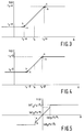
- the saturation function shown in Fig. 3 combined with a suitable correction signal C k actually leads to a optimum determination of the symbols â k .
- Fig. 4 shows a saturation function equivalent to that of Fig. 3.
- the saturation function as shown in Fig. 4 may be derived from the saturation function by scaling all the signals from Fig. 2 by a factor of ⁇ / ⁇ and replacing the difference metric ⁇ ⁇ k-1 by a derived difference metric ⁇ ' k-1 which is equal to ⁇ ⁇ ⁇ k-1 / ⁇ + ⁇ r k .
- ⁇ the correction parameter according to the inventive idea
- ⁇ is equal to ( ⁇ - ⁇ )/ ⁇ .
- the relation between ⁇ ' k-1 and ⁇ ' k as well as the associated extensions of the survivors will be given in the Table below.
- the correction signal is here dual to ⁇ r k .
- Fig. 5 shows aother possible saturation function.
- the L1 norm in lieu of the L2 norm is stared from.
- the L1 norm is equal to the absolute value of its argument in this case being the difference between the expected value of the signal r k for a specific survivor and the really occurring value of r k .
- the Table corresponding to Fig. 5 will be given below.
- the correction signal is now only present if no merge occurs (m0).
- the saturation function degenerates according to Table 4 to a constant value of + ⁇ or - ⁇ respectively.
- an input carrying the signal ⁇ ⁇ k-1 is connected to a positive input of a comparator 34, a negative input of a comparator 36 and a first contact of a switch 42.
- An input carrying input signal r k is connected to a first input of a adder circuit 30 and to a first input of subtracter circuit 32.
- a second input of the adder circuit 30 is supplied with a estimate of the channel parameter ⁇ [ ⁇ ] if the saturation function as shown in Fig. 3 [Fig. 4] is realised.
- a second (negative) input of the subtracter circuit 32 is also supplied with a estimate of the channel parameter ⁇ [ ⁇ ].
- the output of the adder circuit 30 is connected to a negative input of the comparator 34 and to a first contact of the switch 40.
- the output of the subtracter circuit 32 is connected to a positive input of the comparator 36 and to a first contact of the switch 44.
- the output of the comparator 34 carrying output signal m+ is connected to a first input of a NOR-gate 38 and to a control input of the switch 40.
- the output of the comparator 36 carrying output signal m ⁇ is connected to a second input of the NOR-gate 38 and to a control input of the switch 44.
- the output of the NOR-gate 38 carrying output signal m0 is connected to a control input of the switch 42.
- a second contact of each one of the switches 40,42 and 44 is connected to a common junction at which the output signal of the function generator 18 is available.
- the output of the comparator 34 will be active if the signal ⁇ ⁇ k-1 exceeds r k + ⁇ .
- the output of comparator 36 can never be active in this situation, because r k - ⁇ is always smaller than r k + ⁇ for a positive ⁇ . Since the signal m+ is active, the output signal m0 cannot be active. Since signal m+ is active, the switch 40 is closed and the output signal of the function generator is equal to r k + ⁇ .
- the output of the comparator 36 will be active if the signal ⁇ ⁇ k-1 is smaller than r k - ⁇ .
- the output of comparator 34 can never be active in this situation, because r k - ⁇ is always smaller than r k + ⁇ for a positive ⁇ . Since the signal m ⁇ is active, the output signal m0 cannot be active. As a result of the signal m ⁇ being active, the switch 44 is closed and the output signal of the function generator is equal to r k - ⁇ .
- the input signal r k is applied to an input of a memory circuit 50, to a negative input of a subtracter circuit 52, to a first input of an adder circuit 56 and to a first input of an adder circuit 58.
- An output of the adder circuit 58 is connected to the input of a memory 60.
- the output of the memory 60 is connected to a break contact of a change-over switch 68 and a second input of the adder circuit 58.
- the active contact of the change-over switch 68 is connected to a point of constant potential which represents a signal having a reference value 0.
- the central contact of the change-over switch 68 is connected to a second input of the adder circuit 56.
- the output of the adder circuit 56 is connected to a first input of a multiplier circuit 54.
- a second input of the multiplier circuit 54 is supplied with a estimate of the channel parameter ⁇ .
- the output of the multiplier circuit 54 is connected to a first positive input of the subtracter circuit 52.
- An output of the memory circuit 50 carrying output signal r p is connected to a second positive input of the subtracter circuit 52.
- the output of the subtracter circuit 52 is connected to a negative input of a comparator 62 and a positive input of a comparator 64.
- a positive input of the comparator 62 is connected to the central contact of a change-over switch 72.
- a negative input of the comparator 64 is connected to the point of constant potential.
- the output of the comparator 62 carrying output signal B is connected to a first input of an EXCLUSIVE OR-gate 70 and to a first input of a AND-gate 80.
- the output of the comparator 64 carrying output signal A is connected to a input of a flipflop 74, a second input of the EXCLUSIVE OR-gate 70 and a first input of an AND-gate 78.
- the output of the EXCLUSIVE OR-gate 70 carrying output signal u k is connected to a clock input of the flipflop 74, an input of a inverter 76, the control input of the change-over switch 68, a second input of the AND-gate 78, a second input of an AND-gate 80 and to a reset input of the memory 60.
- the output of the flipflop 74 is connected to a control input of the change-over switch 72.
- An estimate of the channel parameter ⁇ is applied to a break contact of the change-over switch 72, whereas the sign-inverted estimate of ⁇ is applied to a active contact of the change-over switch 72.
- the signal m0 is available.
- the signal m+ is available, whereas the output of the AND-gate 80 presents the signal m ⁇ .
- the signal r p is saved by means of memory 50. If there is a merge, the clock input of memory 50 is activated and the value of r k then valid is taken over as the new value r p .
- the adder circuit 58, the memory 60, the switch 68, the adder circuit 56 and the multiplier circuit 54 assist in determining the correction signal.
- the output of the memory 60 presents the sum of the values of r k that have occurred after the most recent merge.
- This output signal may be written as: If there is no merge (m0), the correction signal is equaI to: If there has been a merge (m+ or m ⁇ ), the correction signal C k is equaI to ⁇ r k , because the change-over switch 68 is switched to a reference voltage which represents a zero signal.
- the signal r p -r k +C k is then available at the negative input of the comparator 62 and at the positive input of the comparator 64.
- the value of +2 ⁇ is available at the positive input of the comparator 62 if the most recent merge has been a m+ merge, and the value of -2 ⁇ if the most recent merge has been an m ⁇ merge.
- the output signals of the respective comparators 62 and 64 remain the same and the signal u k remains inactive. In that case there has been no merge (m0). As a result, r p and ⁇ p retain their previous value.
- the correction signal is adapted according to (8) .
- the output signal of the inverter 76 is active and shows that there has been no merge.
- the output signal of the comparator 62 is inactive and the output signal of the comparator 64 is active.
- the output of the EXCLUSIVE OR-gate 70 is then also active. In that case there has been a positive merge (m+).
- the logic value of the signal A is clocked with the signal u k in the flipflop 74, so that ⁇ is now equal to +1.
- the switch 72 is switched to the input signal +2 ⁇ .
- the switch 68 is also switched, so that the next correction signal equals ⁇ r k .
- the memory 60 is reset, so that the summation of r k may now start from the new value of p.
- the output signal of the AND-gate 78 is now active to denote that there has been a positive merge.
- the signal m+ is applied to a first contact of a switch 92, a potential corresponding to a signal equal to 0 is applied to a first contact of a switch 94 and the signal (m ⁇ ) is applied to a switch 96 via an inverter 90.
- the signals m+ and m ⁇ are the output signals of the respective comparators 34 and 36 shown in Fig. 6 or the output signals m++ or m ⁇ respectively, shown in Fig. 7.
- a second contact of the switches 92,94 and 96 is connected to a first input of a multiplier circuit 98.
- a multiplication factor ⁇ is applied to a second input of the multiplier circuit 98.
- the output of the multiplier circuit 98 is connected to a first input of a adder circuit 100.
- the output of the adder circuit 100 is connected to the input of a memory 102, whereas the output of the memory 102 is connected to a second input of the adder circuit 100.
- a signal a+ k is applied to a break contact of a change-over switch 104, whereas a signal a ⁇ k is applied to an active contact of the change-over switch 104.
- a signal a+ k-1 is applied to a break contact of a change-over switch 106, whereas a signal a ⁇ k-1 is applied to an active contact of the change-over switch 106.
- the signals a+ k , a ⁇ k , a+ k-1 and a ⁇ k-1 originate from the two shift registers 22 and 20 in Fig. 2.
- the central contacts of the switches 104 and 106 are connected each to an associated input of a NOR-gate 110 and to an associated input of an AND-gate 111.
- the output of gate 110 is connected to a first input of an AND-gate 112.
- the output of AND-gate 111 is connected to a first input of a AND-gate 114.
- a second input of the AND-gate 112 is supplied with the signal m+, whereas a second input of the AND-gate 114 is supplied with the signal m ⁇ .
- the output of the AND-gate 112 is connected to a control input of the switch 92.
- the output of the AND-gate 114 is connected to a control input of the switch 96.
- the signal m0 is applied to the control input of the switch 94.
- the signal ⁇ k coming from the output of the memory circuit 14 in Fig. 2 is applied to a decision circuit 108.
- the output of the decision circuit 108 is connected to control inputs of the switches 104 and 106.
- This error signal may again be used for adapting the estimated value of ⁇ .
- the error signal determined in (11) also its sign may be used for determining the error signal.
- the advantage of this is that the signs of d k + and d k ⁇ are immediately available in the form of the signals m+ and m ⁇ respectively, whilst these signals may adopt the value of +1 and -1 respectively.
- the control signals Q, m0 and R determine which of the switches 92,94 or 96 is closed. If there has been no merge at the instant k-1, switch 94 is closed and no adaptation of is made. If signal Q or signal R respectively, is active, switch 92 or 96 respectively, is closed. Due to the presence of the inverter 90, there is a signal according to (11) available at the input of the multiplier circuit 98 in both situations.
- the multiplier circuit 98, the adder circuit 100 and the memory form the implementation of the prior-art sign algorithm for determining .
- the AND-gate 112 produces the signal A if there has been a positive merge and if the two most recent symbols of the most likely survivor were equal to -1.
- the two most recent symbols of the most likely survivor are available at the central contacts of the change-over switches 104 and 106.
- the most likely survivor is determined by taking the sign of the signal ⁇ k by means of the decision switch 108.
- the output signal of this decision switch 108 activates the switches 104 and 106 so that the most recent symbols of the most likely survivor are connected to the central contacts of the switches 104 and 106.
- an estimate of ⁇ may be obtained by: Since is often considerably smaller than 1, (15) may be approximated by: A further simplification is obtained by the use of the sign algorithm. (16) then changes into: may be determined with the aid of the LMS algorithm for which ⁇ e k â k may be used as an adaptation signal. If is limited to powers of 2, not the LMS or sign algorithm may be used for the adaptive determination, because in that case the minor adaptations bring ⁇ outside the set of permitted values.
- a solution to this is determining an average over N values of e k â k where N is of the order of 100 to 1000. If this average lies above a first threshold, is increased by a factor of 2 and if this average lies below a second threshold, is reduced by a factor of 2. This increasing or reducing may be simply effected by a shift operation. In this manner will eventually obtain the value at which the mean squared value of the error signal is minimized.
- the channel has an impulse response that has a size exceeding two symbol intervals, it is possible to combine the relatively simple Viterbi detector with a decision feedback circuit.
- Combining a Viterbi detector with a decision feedback circuit is known per se from the journal article "On the use of decision feedback for simplifying the Viterbi detector” by J.W.M. Bergmans et al., in Philips Journal of Research, Vol. 42, No. 4, 1987, pp. 399-428.
Landscapes
- Physics & Mathematics (AREA)
- Probability & Statistics with Applications (AREA)
- Engineering & Computer Science (AREA)
- Theoretical Computer Science (AREA)
- Error Detection And Correction (AREA)
Priority Applications (1)
| Application Number | Priority Date | Filing Date | Title |
|---|---|---|---|
| EP19930201868 EP0580199B1 (fr) | 1992-07-03 | 1993-06-28 | Détecteur Viterbi adaptatif |
Applications Claiming Priority (3)
| Application Number | Priority Date | Filing Date | Title |
|---|---|---|---|
| EP92202028 | 1992-07-03 | ||
| EP92202028 | 1992-07-03 | ||
| EP19930201868 EP0580199B1 (fr) | 1992-07-03 | 1993-06-28 | Détecteur Viterbi adaptatif |
Publications (2)
| Publication Number | Publication Date |
|---|---|
| EP0580199A1 true EP0580199A1 (fr) | 1994-01-26 |
| EP0580199B1 EP0580199B1 (fr) | 1997-03-12 |
Family
ID=26131533
Family Applications (1)
| Application Number | Title | Priority Date | Filing Date |
|---|---|---|---|
| EP19930201868 Expired - Lifetime EP0580199B1 (fr) | 1992-07-03 | 1993-06-28 | Détecteur Viterbi adaptatif |
Country Status (1)
| Country | Link |
|---|---|
| EP (1) | EP0580199B1 (fr) |
Citations (4)
| Publication number | Priority date | Publication date | Assignee | Title |
|---|---|---|---|---|
| EP0155110A2 (fr) * | 1984-02-27 | 1985-09-18 | Nec Corporation | Décodeur Viterbi comprenant un circuit majoritaire pour reproduire un signal décodé |
| US4847871A (en) * | 1987-01-28 | 1989-07-11 | Matsushita Electric Industrial Co., Ltd. | Viterbi detector for digital signal |
| US4868830A (en) * | 1985-09-27 | 1989-09-19 | California Institute Of Technology | Method and apparatus for implementing a traceback maximum-likelihood decoder in a hypercube network |
| US4905317A (en) * | 1986-04-03 | 1990-02-27 | Kabushiki Kaisha Toshiba | Path memory control method in Viterbi decoder |
-
1993
- 1993-06-28 EP EP19930201868 patent/EP0580199B1/fr not_active Expired - Lifetime
Patent Citations (4)
| Publication number | Priority date | Publication date | Assignee | Title |
|---|---|---|---|---|
| EP0155110A2 (fr) * | 1984-02-27 | 1985-09-18 | Nec Corporation | Décodeur Viterbi comprenant un circuit majoritaire pour reproduire un signal décodé |
| US4868830A (en) * | 1985-09-27 | 1989-09-19 | California Institute Of Technology | Method and apparatus for implementing a traceback maximum-likelihood decoder in a hypercube network |
| US4905317A (en) * | 1986-04-03 | 1990-02-27 | Kabushiki Kaisha Toshiba | Path memory control method in Viterbi decoder |
| US4847871A (en) * | 1987-01-28 | 1989-07-11 | Matsushita Electric Industrial Co., Ltd. | Viterbi detector for digital signal |
Also Published As
| Publication number | Publication date |
|---|---|
| EP0580199B1 (fr) | 1997-03-12 |
Similar Documents
| Publication | Publication Date | Title |
|---|---|---|
| US5081651A (en) | Maximum likelihood sequence estimation apparatus | |
| EP0363551B1 (fr) | Egaliseur adaptif pour des systèmes d'enregistrement, utilisant la signalisation à réponse partielle | |
| EP0750306B1 (fr) | Méthode de décodage à vraisemblance maximale, et appareil de reproduction d'informations numériques | |
| EP0644661B1 (fr) | Appareil pour traiter des signaux | |
| US4468786A (en) | Nonlinear equalizer for correcting intersymbol interference in a digital data transmission system | |
| JP3638093B2 (ja) | 光ディスクの復号装置 | |
| US5461644A (en) | Adaptive viterbi detector | |
| US7813702B1 (en) | Receiver with dual D.C. noise cancellation circuits | |
| EP0453814B1 (fr) | Système adaptatif d'estimation de réponses impulsionnelles de canal au moyen d'estimation de séquence ayant un maximum de vraisemblance | |
| US5905743A (en) | Apparatus, methods and computer program products for sequential maximum likelihood estimating communications signals using whitening path metrics | |
| EP0577212B1 (fr) | Détecteur Viterbi adaptif | |
| US6819724B2 (en) | Viterbi decoder and Viterbi decoding method | |
| KR100393198B1 (ko) | E2pr4ml방식의등화기를이용한타이밍복원장치,그에따른타이밍복원방법및최종데이터판정장치 | |
| US5581568A (en) | Data detection apparatus | |
| AU731565B2 (en) | A reception method and a receiver | |
| US5892801A (en) | Decision path reduction of M-ary tree-search detector | |
| US20020150175A1 (en) | Method and apparatus for generating reliability information for channel decoding in a radio receiver | |
| EP0580199B1 (fr) | Détecteur Viterbi adaptatif | |
| EP2017965A1 (fr) | Détecteur map coulissant pour canaux de réponse partiels | |
| US5864590A (en) | Procedure for transmission of information on a channel including a system for reception of data signals by sampling using clock signals | |
| US5557638A (en) | Transmission system for multivalued digital symbols | |
| JP2560893B2 (ja) | データ信号受信装置 | |
| US6292510B1 (en) | Automatic equalization method and automatic equalizer | |
| EP0430428A2 (fr) | Estimation de symbole de donnée | |
| KR960014403B1 (ko) | 적응 등화기의 탭 계수 갱신 제어 시스템 |
Legal Events
| Date | Code | Title | Description |
|---|---|---|---|
| PUAI | Public reference made under article 153(3) epc to a published international application that has entered the european phase |
Free format text: ORIGINAL CODE: 0009012 |
|
| AK | Designated contracting states |
Kind code of ref document: A1 Designated state(s): AT DE FR GB IT |
|
| 17P | Request for examination filed |
Effective date: 19940629 |
|
| RAP1 | Party data changed (applicant data changed or rights of an application transferred) |
Owner name: N.V. PHILIPS' GLOEILAMPENFABRIEKEN |
|
| GRAG | Despatch of communication of intention to grant |
Free format text: ORIGINAL CODE: EPIDOS AGRA |
|
| 17Q | First examination report despatched |
Effective date: 19960430 |
|
| GRAH | Despatch of communication of intention to grant a patent |
Free format text: ORIGINAL CODE: EPIDOS IGRA |
|
| GRAH | Despatch of communication of intention to grant a patent |
Free format text: ORIGINAL CODE: EPIDOS IGRA |
|
| GRAA | (expected) grant |
Free format text: ORIGINAL CODE: 0009210 |
|
| AK | Designated contracting states |
Kind code of ref document: B1 Designated state(s): AT DE FR GB IT |
|
| PG25 | Lapsed in a contracting state [announced via postgrant information from national office to epo] |
Ref country code: AT Effective date: 19970312 |
|
| REF | Corresponds to: |
Ref document number: 150235 Country of ref document: AT Date of ref document: 19970315 Kind code of ref document: T |
|
| REF | Corresponds to: |
Ref document number: 69308672 Country of ref document: DE Date of ref document: 19970417 |
|
| ITF | It: translation for a ep patent filed | ||
| ET | Fr: translation filed | ||
| PLBE | No opposition filed within time limit |
Free format text: ORIGINAL CODE: 0009261 |
|
| STAA | Information on the status of an ep patent application or granted ep patent |
Free format text: STATUS: NO OPPOSITION FILED WITHIN TIME LIMIT |
|
| 26N | No opposition filed | ||
| PGFP | Annual fee paid to national office [announced via postgrant information from national office to epo] |
Ref country code: GB Payment date: 19980601 Year of fee payment: 6 |
|
| PGFP | Annual fee paid to national office [announced via postgrant information from national office to epo] |
Ref country code: FR Payment date: 19980623 Year of fee payment: 6 |
|
| PGFP | Annual fee paid to national office [announced via postgrant information from national office to epo] |
Ref country code: DE Payment date: 19980824 Year of fee payment: 6 |
|
| REG | Reference to a national code |
Ref country code: FR Ref legal event code: CD |
|
| PG25 | Lapsed in a contracting state [announced via postgrant information from national office to epo] |
Ref country code: GB Free format text: LAPSE BECAUSE OF NON-PAYMENT OF DUE FEES Effective date: 19990628 |
|
| PG25 | Lapsed in a contracting state [announced via postgrant information from national office to epo] |
Ref country code: FR Free format text: THE PATENT HAS BEEN ANNULLED BY A DECISION OF A NATIONAL AUTHORITY Effective date: 19990630 |
|
| GBPC | Gb: european patent ceased through non-payment of renewal fee |
Effective date: 19990628 |
|
| PG25 | Lapsed in a contracting state [announced via postgrant information from national office to epo] |
Ref country code: DE Free format text: LAPSE BECAUSE OF NON-PAYMENT OF DUE FEES Effective date: 20000503 |
|
| REG | Reference to a national code |
Ref country code: FR Ref legal event code: ST |
|
| PG25 | Lapsed in a contracting state [announced via postgrant information from national office to epo] |
Ref country code: IT Free format text: LAPSE BECAUSE OF NON-PAYMENT OF DUE FEES Effective date: 20050628 |