EP0580980A1 - Procédé de séchage à la vapeur - Google Patents
Procédé de séchage à la vapeur Download PDFInfo
- Publication number
- EP0580980A1 EP0580980A1 EP93108329A EP93108329A EP0580980A1 EP 0580980 A1 EP0580980 A1 EP 0580980A1 EP 93108329 A EP93108329 A EP 93108329A EP 93108329 A EP93108329 A EP 93108329A EP 0580980 A1 EP0580980 A1 EP 0580980A1
- Authority
- EP
- European Patent Office
- Prior art keywords
- vapor
- semiconductor substrate
- tank
- isopropyl alcohol
- drying
- Prior art date
- Legal status (The legal status is an assumption and is not a legal conclusion. Google has not performed a legal analysis and makes no representation as to the accuracy of the status listed.)
- Withdrawn
Links
Images
Classifications
-
- H—ELECTRICITY
- H10—SEMICONDUCTOR DEVICES; ELECTRIC SOLID-STATE DEVICES NOT OTHERWISE PROVIDED FOR
- H10P—GENERIC PROCESSES OR APPARATUS FOR THE MANUFACTURE OR TREATMENT OF DEVICES COVERED BY CLASS H10
- H10P70/00—Cleaning of wafers, substrates or parts of devices
- H10P70/10—Cleaning before device manufacture, i.e. Begin-Of-Line process
- H10P70/15—Cleaning before device manufacture, i.e. Begin-Of-Line process by wet cleaning only
-
- H—ELECTRICITY
- H10—SEMICONDUCTOR DEVICES; ELECTRIC SOLID-STATE DEVICES NOT OTHERWISE PROVIDED FOR
- H10P—GENERIC PROCESSES OR APPARATUS FOR THE MANUFACTURE OR TREATMENT OF DEVICES COVERED BY CLASS H10
- H10P50/00—Etching of wafers, substrates or parts of devices
-
- H—ELECTRICITY
- H10—SEMICONDUCTOR DEVICES; ELECTRIC SOLID-STATE DEVICES NOT OTHERWISE PROVIDED FOR
- H10P—GENERIC PROCESSES OR APPARATUS FOR THE MANUFACTURE OR TREATMENT OF DEVICES COVERED BY CLASS H10
- H10P72/00—Handling or holding of wafers, substrates or devices during manufacture or treatment thereof
- H10P72/04—Apparatus for manufacture or treatment
- H10P72/0402—Apparatus for fluid treatment
- H10P72/0406—Apparatus for fluid treatment for cleaning followed by drying, rinsing, stripping, blasting or the like
- H10P72/0408—Apparatus for fluid treatment for cleaning followed by drying, rinsing, stripping, blasting or the like for drying
Definitions
- This invention relates generally to vapor drying, and more specifically to the vapor drying of semiconductor substrates.
- Vapor drying of semiconductor substrates with isopropyl alcohol (IPA) is widely used in the semiconductor industry.
- semiconductor substrates wet with deionized water, are introduced into a quartz tank containing a cloud of vaporized IPA.
- the substrates are typically oriented vertically, in a front-to-back relationship.
- a resistive heater mounted to the bottom of the quartz tank, is used to heat a reservoir of liquefied IPA and thus generate the IPA vapor cloud.
- IPA condenses out on the substrates and forms an azeotropic mixture with the de-ionized water.
- the azeotropic mixture has a reduced surface tension that allows it to flow off the substrates, and thus remove de-ionized water from the semiconductor substrates.
- the semiconductor substrates are not always adequately dried by this process.
- the introduction of the wet semiconductor substrates into the quartz tank causes the IPA vapor cloud to collapse or reequilibrate through condensation.
- the IPA vapor cloud is restored first at the bottom of the quartz tank, which is closest to the resistive heat source. Consequently, the azeotropic mixture, which is essential to the drying process, is formed first on those portions of the semiconductor substrate that are located near the bottom of the tank.
- the azeotropic mixture progresses upward on the substrates, in tandem with the restored IPA vapor cloud.
- the semiconductor substrates are dried in a bottom to top manner.
- the restored IPA vapor cloud does not always come into contact with the de-ionized water on the upper portions of the semiconductor substrates, and subsequently form an azeotropic mixture, before the de-ionized water evaporates, forming water spots on the upper portions of the semiconductor substrate. These water spots negatively affect semiconductor device yields and reliability. Additionally, this problem is aggravated by the ever increasing size of semiconductor substrates. Accordingly, a need exists for an IPA vapor drying process that uniformly and reproducibly dries semiconductor substrates, independent of their size.
- an object is vapor dried by placing the object within a tank.
- the object has a top and a bottom.
- the object is exposed to a vapor of a drying medium.
- the vapor of the drying medium is directed toward both the top and the bottom of the object.
- the vapor of the drying medium condenses on and drips from the bottom of the object, carrying away another liquid that was present on the object.
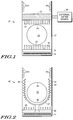
- FIG. 1 illustrates, in cross-section, a vapor drying system suitable for implementing a process in accordance with one embodiment of the invention.
- FIG. 2 illustrates, in cross-section, a vapor drying system suitable for implementing a process in accordance with another embodiment of the invention.
- FIG. 1 Shown in FIG. 1 is a portion 10 of a vapor drying system comprising a quartz tank 12, a resistive heater 14, a liquefied drying medium 16, drying medium vapors 18 and 19, a semiconductor substrate 20, a vapor manifold 22, cooling coils 24, and an external vapor source 30.
- Liquefied drying medium 16 is preferably ultra pure isopropyl alcohol.
- a vapor drying process in accordance with one embodiment of the invention entails the following steps.
- a semiconductor substrate 20, which is wet with a liquid, is placed vertically into quartz tank 12.
- Liquefied drying medium 16, which is lying at the bottom surface of quartz tank 12, is heated by resistive heater 14 such that it boils and generates drying medium vapors 18 that are directed toward the bottom portion 26 of semiconductor substrate 20.
- drying medium vapors 19 generated by external vapor source 30 are injected into manifold 22 and directed toward the top portion 28 of semiconductor substrate 20. Drying medium vapors 18 and 19 condense on semiconductor substrate 20 and form an azeotropic mixture with the liquid originally present on semiconductor substrate 20. The azeotropic mixture drips from the bottom portion 26 of semiconductor substrate 20 and is carried to a drain, removing the liquid that was originally present on semiconductor substrate 20. When drying medium vapors 18 and 19 no longer condense on semiconductor substrate 20, then semiconductor substrate 20 is removed from the vapor drying system.
- FIG. 2 Shown in FIG. 2 is a portion 40 of a vapor drying system comprising a quartz tank 42, a resistive heater 44, a liquefied drying medium 46, drying medium vapors 48, a semiconductor substrate 50, cooling coils 54, and a perforated quartz insert 52.
- Liquefied drying medium 46 is preferably ultra pure isopropyl alcohol.
- a vapor drying process in accordance with a second embodiment of the invention entails the following steps.
- a semiconductor substrate 50 which is wet with a liquid, is placed vertically into quartz tank 42 and within perforated quartz insert 52.
- Liquefied drying medium 46 which is lying at the bottom surface of quartz tank 42, is heated by resistive heater 44 such that it boils and generates drying medium vapors 48.
- Drying medium vapors 48 are guided by perforated quartz insert 52 such that the vapor flow is directed toward both the bottom portion 56 and the top portion 58 of semiconductor substrate 50, as shown in FIG. 2.
- the bottom portion of perforated quartz insert 52 is not perforated so that drying medium vapor 48 is forced to move upward and is channeled around semiconductor substrate 50.
- Drying medium vapors 48 condense on semiconductor substrate 50 and form an azeotropic mixture with the liquid originally present on semiconductor substrate 50.
- the azeotropic mixture drips from the bottom portion 56 of semiconductor substrate 50 and is carried to a drain, removing the liquid that was originally present on semiconductor substrate 50.
- semiconductor substrate 50 is removed from the vapor drying system.
- One advantage is that vapor from the drying medium contacts both the upper and lower portions of the semiconductor substrate nearly simultaneously. Consequently, vapor condensation and the subsequent formation of the azeotropic mixture occurs rapidly on both the upper and lower portions of the semiconductor substrate at essentially the same time.
- the entire semiconductor substrate is quickly covered by the azeotropic mixture, which is essential to the drying process, and the semiconductor substrate is uniformly dried.
- this multi-directional drying process allow large semiconductor substrates to be dried, but it also minimizes the time required to dry them.
Landscapes
- Cleaning Or Drying Semiconductors (AREA)
- Drying Of Solid Materials (AREA)
Applications Claiming Priority (2)
| Application Number | Priority Date | Filing Date | Title |
|---|---|---|---|
| US920074 | 1992-07-27 | ||
| US07/920,074 US5351419A (en) | 1992-07-27 | 1992-07-27 | Method for vapor drying |
Publications (1)
| Publication Number | Publication Date |
|---|---|
| EP0580980A1 true EP0580980A1 (fr) | 1994-02-02 |
Family
ID=25443110
Family Applications (1)
| Application Number | Title | Priority Date | Filing Date |
|---|---|---|---|
| EP93108329A Withdrawn EP0580980A1 (fr) | 1992-07-27 | 1993-05-24 | Procédé de séchage à la vapeur |
Country Status (4)
| Country | Link |
|---|---|
| US (1) | US5351419A (fr) |
| EP (1) | EP0580980A1 (fr) |
| JP (1) | JPH0697149A (fr) |
| KR (1) | KR940002965A (fr) |
Cited By (1)
| Publication number | Priority date | Publication date | Assignee | Title |
|---|---|---|---|---|
| WO2005004217A1 (fr) * | 2003-07-02 | 2005-01-13 | S.E.S. Co., Ltd. | Procede et dispositif de traitement d'un substrat |
Families Citing this family (17)
| Publication number | Priority date | Publication date | Assignee | Title |
|---|---|---|---|---|
| US5660642A (en) * | 1995-05-26 | 1997-08-26 | The Regents Of The University Of California | Moving zone Marangoni drying of wet objects using naturally evaporated solvent vapor |
| US5653045A (en) * | 1995-06-07 | 1997-08-05 | Ferrell; Gary W. | Method and apparatus for drying parts and microelectronic components using sonic created mist |
| KR100189779B1 (ko) * | 1995-12-04 | 1999-06-01 | 윤종용 | 웨이퍼의 건조장치 |
| US5815942A (en) * | 1996-12-13 | 1998-10-06 | Kabushiki Kaisha Toshiba | Vapor drying system and method |
| KR100434714B1 (ko) * | 1997-04-18 | 2004-10-14 | 주식회사 하이닉스반도체 | 웨이퍼건조장치 |
| JP3230051B2 (ja) * | 1997-05-16 | 2001-11-19 | 東京エレクトロン株式会社 | 乾燥処理方法及びその装置 |
| JPH11162876A (ja) * | 1997-11-28 | 1999-06-18 | Nec Corp | 半導体装置の製造装置及び製造方法 |
| US6289605B1 (en) * | 2000-02-18 | 2001-09-18 | Macronix International Co. Ltd. | Method for drying a semiconductor wafer |
| US7364625B2 (en) * | 2000-05-30 | 2008-04-29 | Fsi International, Inc. | Rinsing processes and equipment |
| US6589361B2 (en) | 2000-06-16 | 2003-07-08 | Applied Materials Inc. | Configurable single substrate wet-dry integrated cluster cleaner |
| US6519869B2 (en) * | 2001-05-15 | 2003-02-18 | United Microelectronics, Corp. | Method and apparatus for drying semiconductor wafers |
| US6899111B2 (en) * | 2001-06-15 | 2005-05-31 | Applied Materials, Inc. | Configurable single substrate wet-dry integrated cluster cleaner |
| US6398875B1 (en) | 2001-06-27 | 2002-06-04 | International Business Machines Corporation | Process of drying semiconductor wafers using liquid or supercritical carbon dioxide |
| US20040031167A1 (en) | 2002-06-13 | 2004-02-19 | Stein Nathan D. | Single wafer method and apparatus for drying semiconductor substrates using an inert gas air-knife |
| US20080289660A1 (en) * | 2007-05-23 | 2008-11-27 | Air Products And Chemicals, Inc. | Semiconductor Manufacture Employing Isopropanol Drying |
| US9275849B2 (en) * | 2007-07-30 | 2016-03-01 | Planar Semiconductor, Inc. | Single-chamber apparatus for precision cleaning and drying of flat objects |
| US9418831B2 (en) * | 2007-07-30 | 2016-08-16 | Planar Semiconductor, Inc. | Method for precision cleaning and drying flat objects |
Citations (2)
| Publication number | Priority date | Publication date | Assignee | Title |
|---|---|---|---|---|
| JPS63266833A (ja) * | 1987-04-24 | 1988-11-02 | Hitachi Ltd | 乾燥装置 |
| GB2224639A (en) * | 1988-11-15 | 1990-05-16 | Canon Kk | Vapor cleaning method |
Family Cites Families (2)
| Publication number | Priority date | Publication date | Assignee | Title |
|---|---|---|---|---|
| JPH02110929A (ja) * | 1988-10-20 | 1990-04-24 | Hitachi Electron Eng Co Ltd | ベーパ乾燥装置 |
| JP2752001B2 (ja) * | 1990-10-19 | 1998-05-18 | 株式会社日立製作所 | 蒸気乾燥装置 |
-
1992
- 1992-07-27 US US07/920,074 patent/US5351419A/en not_active Expired - Fee Related
-
1993
- 1993-05-24 EP EP93108329A patent/EP0580980A1/fr not_active Withdrawn
- 1993-06-04 KR KR1019930010024A patent/KR940002965A/ko not_active Withdrawn
- 1993-07-23 JP JP5202062A patent/JPH0697149A/ja active Pending
Patent Citations (2)
| Publication number | Priority date | Publication date | Assignee | Title |
|---|---|---|---|---|
| JPS63266833A (ja) * | 1987-04-24 | 1988-11-02 | Hitachi Ltd | 乾燥装置 |
| GB2224639A (en) * | 1988-11-15 | 1990-05-16 | Canon Kk | Vapor cleaning method |
Non-Patent Citations (1)
| Title |
|---|
| PATENT ABSTRACTS OF JAPAN vol. 013, no. 088 (E-721)28 February 1989 & JP-A-63 266 833 ( SAKURAI TOSHIHIKO ) 2 November 1988 * |
Cited By (3)
| Publication number | Priority date | Publication date | Assignee | Title |
|---|---|---|---|---|
| WO2005004217A1 (fr) * | 2003-07-02 | 2005-01-13 | S.E.S. Co., Ltd. | Procede et dispositif de traitement d'un substrat |
| CN100380602C (zh) * | 2003-07-02 | 2008-04-09 | S.E.S.株式会社 | 衬底处理方法和衬底处理装置 |
| US7648580B2 (en) | 2003-07-02 | 2010-01-19 | S.E.S. Co., Ltd. | Substrate processing method and substrate processing device |
Also Published As
| Publication number | Publication date |
|---|---|
| KR940002965A (ko) | 1994-02-19 |
| JPH0697149A (ja) | 1994-04-08 |
| US5351419A (en) | 1994-10-04 |
Similar Documents
| Publication | Publication Date | Title |
|---|---|---|
| US5351419A (en) | Method for vapor drying | |
| US5951779A (en) | Treatment method of semiconductor wafers and the like and treatment system for the same | |
| US20120260517A1 (en) | Apparatus and Method for Reducing Substrate Pattern Collapse During Drying Operations | |
| US20090229637A1 (en) | Method of preventing pattern collapse during rinsing and drying | |
| KR100481858B1 (ko) | 공비혼합 효과를 이용하여 반도체기판을 건조시키는 장비및 상기 장비를 사용하는 건조방법 | |
| US6598312B2 (en) | Wafer drying apparatus | |
| US5688410A (en) | Method of ashing resist and apparatus therefor | |
| JPH01287928A (ja) | 蒸気乾燥方法及びその装置 | |
| US6695926B1 (en) | Treatment method of semiconductor wafers and the like and treatment system for the same | |
| JPS63182818A (ja) | 乾燥装置 | |
| US6101737A (en) | Apparatus and method for drying a semiconductor member | |
| JP2511873B2 (ja) | ベ−パ乾燥装置 | |
| KR980011979A (ko) | 웨이퍼 세정/건조 장치 및 방법 | |
| JP3009006B2 (ja) | 半導体基板の乾燥装置 | |
| JP2023084770A (ja) | 溶剤蒸気供給装置及び溶剤蒸気供給方法 | |
| JPS62159433A (ja) | レジスト除去方法及び装置 | |
| US6055743A (en) | Method and apparatus for drying semiconductor wafers without forming water markers thereon | |
| JP2003092256A (ja) | 基板処理装置及び基板処理方法 | |
| KR0180344B1 (ko) | 반도체 웨이퍼의 건조장치 | |
| TW200301928A (en) | Apparatus and methods for processing electronic component precursors | |
| US6519869B2 (en) | Method and apparatus for drying semiconductor wafers | |
| JPH11102891A (ja) | 基板処理装置 | |
| JPS61241927A (ja) | 蒸気乾燥装置 | |
| JPS63266833A (ja) | 乾燥装置 | |
| JP2002502109A (ja) | 基板の乾燥法および乾燥装置 |
Legal Events
| Date | Code | Title | Description |
|---|---|---|---|
| PUAI | Public reference made under article 153(3) epc to a published international application that has entered the european phase |
Free format text: ORIGINAL CODE: 0009012 |
|
| AK | Designated contracting states |
Kind code of ref document: A1 Designated state(s): DE FR GB IT |
|
| 18D | Application deemed to be withdrawn |
Effective date: 19940803 |