EP0581085A1 - Strahlungsgeschützte CMOS-Struktur durch implantierten Schutzring vom P-Typ und Verfahren zur Herstellung - Google Patents
Strahlungsgeschützte CMOS-Struktur durch implantierten Schutzring vom P-Typ und Verfahren zur Herstellung Download PDFInfo
- Publication number
- EP0581085A1 EP0581085A1 EP93111024A EP93111024A EP0581085A1 EP 0581085 A1 EP0581085 A1 EP 0581085A1 EP 93111024 A EP93111024 A EP 93111024A EP 93111024 A EP93111024 A EP 93111024A EP 0581085 A1 EP0581085 A1 EP 0581085A1
- Authority
- EP
- European Patent Office
- Prior art keywords
- area
- field oxide
- well
- spaced
- rad
- Prior art date
- Legal status (The legal status is an assumption and is not a legal conclusion. Google has not performed a legal analysis and makes no representation as to the accuracy of the status listed.)
- Withdrawn
Links
Images


Classifications
-
- H—ELECTRICITY
- H10—SEMICONDUCTOR DEVICES; ELECTRIC SOLID-STATE DEVICES NOT OTHERWISE PROVIDED FOR
- H10D—INORGANIC ELECTRIC SEMICONDUCTOR DEVICES
- H10D84/00—Integrated devices formed in or on semiconductor substrates that comprise only semiconducting layers, e.g. on Si wafers or on GaAs-on-Si wafers
- H10D84/80—Integrated devices formed in or on semiconductor substrates that comprise only semiconducting layers, e.g. on Si wafers or on GaAs-on-Si wafers characterised by the integration of at least one component covered by groups H10D12/00 or H10D30/00, e.g. integration of IGFETs
- H10D84/82—Integrated devices formed in or on semiconductor substrates that comprise only semiconducting layers, e.g. on Si wafers or on GaAs-on-Si wafers characterised by the integration of at least one component covered by groups H10D12/00 or H10D30/00, e.g. integration of IGFETs of only field-effect components
- H10D84/83—Integrated devices formed in or on semiconductor substrates that comprise only semiconducting layers, e.g. on Si wafers or on GaAs-on-Si wafers characterised by the integration of at least one component covered by groups H10D12/00 or H10D30/00, e.g. integration of IGFETs of only field-effect components of only insulated-gate FETs [IGFET]
- H10D84/85—Complementary IGFETs, e.g. CMOS
-
- H—ELECTRICITY
- H10—SEMICONDUCTOR DEVICES; ELECTRIC SOLID-STATE DEVICES NOT OTHERWISE PROVIDED FOR
- H10W—GENERIC PACKAGES, INTERCONNECTIONS, CONNECTORS OR OTHER CONSTRUCTIONAL DETAILS OF DEVICES COVERED BY CLASS H10
- H10W10/00—Isolation regions in semiconductor bodies between components of integrated devices
- H10W10/01—Manufacture or treatment
- H10W10/011—Manufacture or treatment of isolation regions comprising dielectric materials
- H10W10/012—Manufacture or treatment of isolation regions comprising dielectric materials using local oxidation of silicon [LOCOS]
- H10W10/0125—Manufacture or treatment of isolation regions comprising dielectric materials using local oxidation of silicon [LOCOS] comprising introducing electrical impurities in local oxidation regions, e.g. to alter LOCOS oxide growth characteristics
- H10W10/0126—Manufacture or treatment of isolation regions comprising dielectric materials using local oxidation of silicon [LOCOS] comprising introducing electrical impurities in local oxidation regions, e.g. to alter LOCOS oxide growth characteristics introducing electrical active impurities in local oxidation regions to create channel stoppers
- H10W10/0127—Manufacture or treatment of isolation regions comprising dielectric materials using local oxidation of silicon [LOCOS] comprising introducing electrical impurities in local oxidation regions, e.g. to alter LOCOS oxide growth characteristics introducing electrical active impurities in local oxidation regions to create channel stoppers using both n-type and p-type impurities, e.g. for isolation of complementary doped regions
-
- H—ELECTRICITY
- H10—SEMICONDUCTOR DEVICES; ELECTRIC SOLID-STATE DEVICES NOT OTHERWISE PROVIDED FOR
- H10W—GENERIC PACKAGES, INTERCONNECTIONS, CONNECTORS OR OTHER CONSTRUCTIONAL DETAILS OF DEVICES COVERED BY CLASS H10
- H10W10/00—Isolation regions in semiconductor bodies between components of integrated devices
- H10W10/10—Isolation regions comprising dielectric materials
- H10W10/13—Isolation regions comprising dielectric materials formed using local oxidation of silicon [LOCOS], e.g. sealed interface localised oxidation [SILO] or side-wall mask isolation [SWAMI]
-
- Y—GENERAL TAGGING OF NEW TECHNOLOGICAL DEVELOPMENTS; GENERAL TAGGING OF CROSS-SECTIONAL TECHNOLOGIES SPANNING OVER SEVERAL SECTIONS OF THE IPC; TECHNICAL SUBJECTS COVERED BY FORMER USPC CROSS-REFERENCE ART COLLECTIONS [XRACs] AND DIGESTS
- Y10—TECHNICAL SUBJECTS COVERED BY FORMER USPC
- Y10S—TECHNICAL SUBJECTS COVERED BY FORMER USPC CROSS-REFERENCE ART COLLECTIONS [XRACs] AND DIGESTS
- Y10S257/00—Active solid-state devices, e.g. transistors, solid-state diodes
- Y10S257/921—Radiation hardened semiconductor device
-
- Y—GENERAL TAGGING OF NEW TECHNOLOGICAL DEVELOPMENTS; GENERAL TAGGING OF CROSS-SECTIONAL TECHNOLOGIES SPANNING OVER SEVERAL SECTIONS OF THE IPC; TECHNICAL SUBJECTS COVERED BY FORMER USPC CROSS-REFERENCE ART COLLECTIONS [XRACs] AND DIGESTS
- Y10—TECHNICAL SUBJECTS COVERED BY FORMER USPC
- Y10S—TECHNICAL SUBJECTS COVERED BY FORMER USPC CROSS-REFERENCE ART COLLECTIONS [XRACs] AND DIGESTS
- Y10S438/00—Semiconductor device manufacturing: process
- Y10S438/953—Making radiation resistant device
Definitions
- the invention relates to semiconductor processing, and more particularly to fabrication and processing of radiation-hardened CMOS structures.
- CMOS Complementary Metal Oxide Semiconductor
- CMOS processes (2 micron line widths and below).
- Two of the biggest advantages of CMOS technology are: 1) its inherently high noise immunity (due to relatively large voltage differences between CMOS logic output voltages and input switching thresholds compared to other logic families), and 2) low power dissipation.
- CMOS technology is particularly desirable in military and aerospace applications because of these noise and power characteristics.
- military and aerospace environments tend to be characterized by high levels of radiation, particularly gamma and X-ray radiation, and standard CMOS circuits are known to have some problems with high-radiation environments. While it is possible to construct radiation shields for CMOS military applications, this tends to add weight, expense, and complexity; requires extensive testing; and negates much of the desirability of CMOS for these applications.
- CMOS technology is typified by logic gates constructed from complementary pairs of MOS Field Effect Transistors (FET's) (p-channel and n-channel) in a sort of a push-pull configuration where only one transistor of any given pair is "on” at a time, such that CMOS gates (ideally) draw no steady-state current.
- FET's MOS Field Effect Transistors
- IGFETs insulated-gate field effect transistors
- Random-hardness refers to the ability of a semiconductor device to withstand radiation without alteration of its electrical characteristics.
- a semiconductor device is said to be radiation hardened (rad-hard), radiation tolerant, or radiation resistant if it can continue to function within specifications after exposure to a specified amount of radiation.
- Semiconductor devices can be damaged or destroyed by the effects of nuclear radiation from natural and man-made sources. Radiation changes the electrical properties of solid state devices, leading to possible failure of any system incorporating them.
- Rad-hard devices and circuits have been developed to minimize the effects of these forces.
- the devices can be designed to be rad-hard, or the normal manufacturing process can be modified to produce rad-hard devices with special isolation techniques. Radiation hardening now permits systems designers to take advantage of the benefits of CMOS technology in high-performance, high-reliability products intended for applications where radiation is present.
- An alpha particle is a helium nucleus or a helium atom without its electrons. It travels at close to the speed of light, but can be stopped by a sheet of paper.
- a beta particle is an electron traveling at nearly the speed of light. The same as an electron orbiting a nucleus, it differs only in speed.
- the beta particle can travel about 20 feet (6.1 m) in air and is stopped by 1/16 inch (1.6 mm) thick aluminum barriers.
- Ions are charged particles formed when one or more electrons are removed or added to a previously neutral atom or molecule.
- The are, for example, silicon ions.
- Neutrons A neutron is a particle without electric charge. It has a mass that is approximately equal to that of a proton. Neutrons are naturally bound to the nucleus of an atom, but they can be displaced in various types of nuclear interactions.
- Gamma rays are photons or quanta of energy with characteristics that are identical to those of X rays. The difference between gamma rays and X rays is their source. Gamma rays come from the atomic nucleus, but X rays are generated by processes outside the nucleus. Gamma rays and X rays have no electrical charge, travel at the speed of light, and can be stopped by a concrete or lead shield.
- the interactions of a particle with a material will depend on the properties of each.
- the properties of particles are: 1) mass, 2) charge, and 3) kinetic energy.
- the properties of materials are: 1) mass, 2) charge, and 3) density.
- the energy transferred to a material by ionizing radiation is measured in rads (radiation absorbed dose).
- rads radiation absorbed dose
- One rad is equal to the energy of 100 ergs per gram of material.
- the material must be specified, because this energy will differ with each material.
- the ionizing dose rate for silicon- based (Si based) semiconductors is referred to in rads(Si)/second.
- Particles are referred to in terms of concentration as well as the time integral of concentration:
- Neutron radiation presents more problems in bipolar devices than in CMOS devices until a fluence of 10 15 neutrons per square centimeter or greater is reached. Heavily charged particles can cause single event upset.
- Ionization is the principal agent that damages or destroys CMOS devices. It is caused by photon (gamma or X ray) interactions, fast neutron interactions, and charged (alpha and beta) particles. However, of these, gamma and X-radiation are the primary sources of this ionization.
- CMOS devices particularly troublesome to CMOS devices in high radiation environments are active parasitic devices which occur within the CMOS devices themselves, particularly field isolation MOS ("field transistor”, or “parasitic field transistor”; used interchangeably herein) and parasitic SCR (silicon controlled rectifier) structures.
- field isolation MOS field transistor
- parasitic SCR silicon controlled rectifier
- NMOS the n-channel part of the complementary pairs of transistors in CMOS structures
- parasitic SCR latch-up are known to cause fatal (unrecoverable) misoperation of CMOS designs in high radiation environments.
- NMOS field transistor leakage is known to be induced by large negative threshold shifts in parasitic field transistors as a cumulative effect of radiation.
- rad-hard radiation tolerant
- CMOS devices Numerous radiation tolerant (rad-hard) designs of CMOS devices have been proposed and implemented. Typically, these designs are significantly larger and/or slower than their conventional CMOS counterparts. Examples of present techniques for creating rad-hard CMOS devices and the characterization thereof are given in: H. Hatano and Satoru Takatsuka, "Total Dose Radiation-Hardened Latch-up Free CMOS Structures for Radiation-Tolerant VLSI Designs", IEEE Trans. Nucl. Sci., vol NS-33, no.
- HATANO 1 Hiroshi Hatano and Satoru Takatsuka, "Radiation-Tolerant 50MHz Bulk CMOS VLSI Circuits Utilizing Radiation-Hard Structure NMOS transistors", IEEE Trans. Nucl. Sci., vol. NS-33, no. 5, 1986, (hereinafter "HATANO 2"); and I. Yoshii, K. Hama, K Maeguchi, S. Takatsuka, and H. Hatano, “Total-Dose Characterization of a High-Performance Radiation-Hardened 1.0- ⁇ rn CMOS Sea-Of-Gates Technology", (hereinafter "HATANO 3").
- P-, P, and P + used to describe the doping concentrations of P-type dopants
- N-, N, and N + used to describe the doping concentrations of N-type dopants
- P- and N- designations apply to doping concentrations of 10' 4- 10' 6 atoms/cm 3 of P-type and N-type dopants, respectively.
- P and “N” designations apply to doping concentrations of 1 016 -1 019 atoms/cm 3 of P-type and N-type dopants, respectively.
- P + and “N + designations apply to doping concentrations of 10 19- 10 21 atoms/ cm 3 of P-type and N-type dopants, respectively.
- HATANO 1 shows six rad-hard NMOS transistor structures which may be incorporated into CMOS devices, three of which (“Structures 4-6" therein) utilize a P + guard hand structure under thin oxide.
- these three thin oxide “guard” band implementations are shown to have suitable total-dose radiation characteristics, but they suffer from relatively low density and speed compared to the other three structures ("Structures 1-3").
- Structures 4-6 Of the three structures shown as “Structures 4-6" in HATANO 1, “Structure 6" is slightly smaller, and exhibits better speed response. It is this structure which is of primary interest herein.
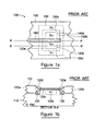
- Figures 1a-1c illustrate "Structure 6" of HATANO 1.
- Figure 1a shows a top view of an NMOS transistor 100 wherein a P+ guard ring 130 and N + source and drain diffusion regions, 140a and 140b, respectively, underlie an oxide layer 120.
- An overlying poly-silicon (“poly") gate structure 150 is shown.
- Guard ring 130 is shown as having two segments 130a and 130b running perpendicular to the gate structure, and two segments 130c and 130d running parallel to the gate structure.
- Two section lines A-A' for which Figure 1 b is a representative section
- B-B' for which Figure 1 c is a representative section
- Figure 1b shows a section A-A' of NMOS transistor 100 wherein the poly-silicon gate 150 is shown overlying thick field oxide layer segment 120a, and a thin gate oxide layer segment 120c.
- Oxide layer segments 120a-c are all components of oxide layer 120 ( Figure 1 a).
- P + guard ring 130 is diffused into a P- well 110 into which the NMOS transistor is fabricated, and is shown as two sections underlying the interfaces between thick oxide layer segments 120a and 120b and thin oxide layer section 120c, 120d and 120e, respectively.
- These interfaces 120d and 120e are commonly called "bird's beak" sections, due to the similarity of their shape to the head and beak of a bird.
- the gate structure 150 does not continue onto thick gate oxide segment 120b, but is "pulled back". This minimizes the possibility of field inversion under oxide layer 120b. While this is advantageous for the purposes of HATANO 1, some CMOS design constraints do not permit the gate to be pulled back, limiting the usefulness of this structure for those applications.
- Figure 1c shows a section B-B' of NMOS transistor 100, away from gate structure 150 and through N + drain (or source) diffusion region 140b. Again, thick field oxide layer sections 120a and 120b, and thin gate oxide section 120c are shown overlying P- well 110, into which P+ guard ring 130 and N + drain diffusion region 140b have been separately diffused.
- the doping density of the P + guard ring 130 in NMOS transistor 100 necessitates a relatively large distance between the N + source and drain diffusion regions (140a and 140b) and the guard ring 130 in order to minimize parasitic capacitances therebetween.
- the fact that guard ring 130 is actually a complete ring also tends to increase the area over which capacitances between the guard ring and source and drain diffusion regions 140a and 140b may occur.
- These parasitic capacitances slow the switching response of the NMOS transistor 100, and any associated CMOS device, accordingly. As a result, significant tradeoffs must be made between transistor speed and size.
- HATANO 1 shows rad-hard Structure 6 ( Figures 1 a-c herein) as being 59% larger (in area) than a similar conventional CMOS gate.
- the additional size is due, at least in part, to the distance it is required to space the P + guard ring (130) away from the source and drain diffusion regions (140a and 140b) so that the effect of parasitic capacitance on device speed will be minimal.
- the portions 130a and 130b of P + guard ring 130 which run perpendicular to the gate 150 compensate primarily for an effect known as “poly field inversion” or “gate field inversion” (activation of active parasitic transistors due to fields from the gate structure).
- the portions 130c and 130d of P + guard ring 130 which run parallel to the gate 150 compensate primarily for an effect known as “metal field inversion” arising from activation of parasitic devices by fields from metal contacts to the source and drain diffusion regions (not shown).
- guard structures have significant advantages in the area of total dose radiation hardness, by virtue of their very effective control of the active parasitic device thresholds.
- CMOS structure characterized by thick field oxide around the NMOS transistors; thin gate oxide over N + source and drain diffusion regions, a channel area under a poly-silicon gate overlying and between the source and drain structures, and relative immunity to metal field inversion (provided by techniques well known to those skilled in the art of semiconductor processing), is prepared up to a point prior to the fabrication of the gate structure.
- a photo-mask is applied and a two-part P (10 18- 10 20 atoms/cm 3 ) guard structure is photo-implanted into each NMOS transistor structure such that each part will immediately underlie one of the two bird's-beak oxide structures running perpendicular to the path of the gate.
- the remaining CMOS device structure is completed normally.
- CMOS structure which is relatively immune to metal field inversion
- the need for the complete guard ring of the prior art e.g., Structure 6 of HATANO 1
- the portion of the ring which runs parallel to the gate structure in Structure 6 of HATANO 1 is not necessary in the present invention.
- This also helps further reduce the size and/or speed of the NMOS transistor by reducing the total parasitic capacitance. By reducing the parasitic capacitance, it is then possible to reduce the spacing between the guard structure and the N + source and drain diffusion regions for the same level of capacitance, further reducing device size. Alternatively a benefit in NMOS transistor speed may be achieved for the same device size.
- the active parasitic device thresholds are still effectively controlled (increased), but the lower doping density permits significantly less distance between the guard structure and the source and drain diffusion regions at the same or lower levels of parasitic capacitance as those in the technique of the prior art.
- a P + doping density for the guard structure (such as that used in the guard ring of Structure 6 of HATANO 1) would be "overkill", and would require significant increases in device size in order to maintain reasonable performance.
- rad-hard CMOS devices can be constructed which exhibit excellent total-dose radiation hardness, perform at speeds comparable to those of normal (non rad-hard) CMOS devices, are comparable in size to normal CMOS devices, and are readily manufacturable, requiring minimal additional implanter time.
- Figures 1a-1c show a prior-art rad-hard NMOS transistor which, when used in a CMOS device, provides good total-dose radiation hardness, but which is substantially larger and somewhat slower than comparable conventional CMOS devices.
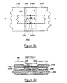
- Figures 2a-2c show different views of an embodiment of a rad-hard NMOS transistor, as it relates to the present invention.
- Figure 2a shows an isometric view of a section of an embodiment of a rad-hard NMOS transistor 200 according to the present invention.
- a P- well 230 into which P doped regions 220a and 220b have been implanted under thick field oxide segments 210a and 210b, respectively.
- a thin gate oxide segment 215 overlies P- well 230 and joins thick gate oxide segments 210a and 210b.
- a poly-silicon gate structure 240 overlies the three oxide segments.
- N + diffusion regions 250a and 250b interchangeably act as source and drain of the NMOS transistor.
- the second N + diffusion region 250b acts as the drain.
- the first N + diffusion region 250a is chosen as the drain, then the second N + diffusion region 250b acts as the source.
- a space between the two N + diffusion regions 250a and 250b in the P- well 230 underlying the poly-silicon gate structure 240 and the thin gate oxide segment 215 acts as a channel area (shown as 290 in Figure 2b) of the NMOS transistor.
- a P guard structure 260a is implanted such that it runs approximately the length of the area covered by the poly-silicon gate structure 240 and the two N + diffusion regions 250a and 250b.
- a similar P guard structure 260b is implanted immediately under the "bird's beak interface (shown as 210d in Figure 2c) between thick field oxide 210b and thin gate oxide 215, and running approximately the same length as P guard structure 260a.
- Figure 2a also shows parasitic field transistor leakage paths as arrows 270a and 270b.
- One parasitic transistor can occur generally along the path shown by arrow 270a.
- the direction of current leakage is dependent upon the polarity of voltages applied to N + diffusion regions 250a and 250b. The direction shown implies that 250a is chosen as the drain, or more positive diffusion region.
- Leakage currents will flow along this path in the event that sufficient field inversion occurs to create a channel in the P- well along the path.
- P doped region 220a protects against this to some degree but, in conventional NMOS transistors, trapped charges under the bird's beak interface between field oxide 210a and gate oxide 215 can cause sufficient inversion of the P- material in the region of the bird's beak interface 210c (effectively lowering the threshold of the parasitic field transistor) to create a leakage path between the two N + diffusion regions 250a and 250b, allowing leakage current to flow. At a minimum, this causes significantly increased power dissipation; at maximum, it can cause misoperation of the device which incorporates the NMOS transistor. This effect is particularly prone to long-term degradation due to cumulative effects of radiation.
- guard band 260a in combination with P doped region 220a substantially increases the threshold of the parasitic field transistor structure by substantially increasing the amount of charge required to cause inversion of the material in this area, dramatically reducing the likelihood of leakages being caused by trapped charges in the bird's beak region.
- a similar parasitic transistor leakage path is shown on the opposite side of the N + diffusion regions by 270b. This parasitic transistor leakage path is effectively compensated by P guard band 260b in a manner similar to that previously described for P guard band 260a.
- Figure 2b shows a top view of the same NMOS transistor structure, more clearly illustrating the area relationships between the gate structure 240, the N + diffusion regions 250a and 250b, and the P guard structures 260a and 260b. All other reference numbers are the same as for Figure 2a and refer to the same features of the NMOS transistor.
- the channel area is generally indicated by 290. This channel area occurs in the P- well immediately below the thin oxide layer 215.
- Figure 2b it can clearly be seen that the two N + diffusion regions 250a and 250b do not extend under the gate structure. This is because the N + diffusion process uses the gate structure as a mask.
- Figure 2b also indicates a section line C-C' through the center line of the gate structure 240, along which line the cross-sectional view in Figure 2c is taken.
- Figure 2c shows a cross-sectional view C-C' of rad-hard NMOS transistor 200 taken along the centerline of gate structure 240. All reference numbers and the structures they represent are the same as for Figures 2a and 2b. Figure 2c more clearly shows the relationship between the gate structure 240, the oxide layer segments 210a, 210b, and 215, the N + diffusion region 250b, the P guard bands 260a and 260b, and the P doped regions 220a and 220b.
- N + diffusion region 250b is shown as a dashed line because the cross-sectional view is taken through the centerline of gate structure 240, under which the N + diffusion regions do not extend.
- the P guard bands 260a and 260b are clearly shown under bird's beak regions 210c and 210d, respectively, and located in (and, by implication, extending through) the region under the gate 240.
- Figures 2a-2c show the structure of a rad-hard NMOS transistor, and the discussion related thereto describes the features and mechanisms by which the transistor is made radiation-hard.
- Figures 3a-d the method of manufacturing a CMOS structure incorporating such a rad-hard NMOS transistor is described.
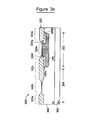
- Figures 3a-3d show cross-sectional views of a rad-hard CMOS structure incorporating the techniques of the invention, at various process steps.
- Figure 3a shows a cross-sectional view of an incomplete typical CMOS structure at a point in the fabrication process before deposition of a gate structure. The plane of this cross-sectional view runs along the center line of the path of the gate structure to be formed overlying the structure shown.
- a substrate material has been chosen comprising a base N + material 360 underlying an N- material 350.
- a P- well 340 has been created.
- Two P structures 330a and 330b are shown implanted into P- well 340 under thick portions 320c and 320e of overlying oxide layer 320 (330a and 330b are similar to 220a and 220b with respect to Figures 2a, 2c).
- Overlying oxide layer 320 has been created, appropriately etched, and processed to form thick oxide segments 320a, 320c, and 320e, and thin oxide segments 320b and 320d, shown in this cross-sectional view.
- Thin oxide segment 320b will act as a thin gate oxide for a PMOS transistor which will be located generally in the region indicated by 204.
- Thin oxide segment 320d will act as a thin gate oxide for an NMOS transistor which will be located generally in the region indicated by 202.
- Bird's beak regions 320f is shown at the interface of thick oxide 320b and thin oxide 320d
- bird's beak region 320g is shown at the interface of thick oxide 320e and thin oxide 320d.
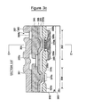
- Figure 3b shows the CMOS structure of Figure 3a after an overlying layer of a patterned photo-resist masking material 310 has been deposited, and during photo implantation by an implantation process 395 of two P guard structures 335a and 335b.
- Photo-resist masking layer 310 has elongated openings 396, through which the implantation occurs.
- thicker portions of thick oxide segments 320c and 320e also tend to act as masks for the implantation process 395, limiting the implantation to the area under bird's beak structures 320f and 320g ( Figure 3a).
- guard bands 335a and 335b are in contact with and conductive to the P material of P structures 330a and 330b.
- Guard bands 335a and 335b are similar to guard bands 260a and 260b with respect to Figures 2a and 2c. Note that these guard bands differ from the guard ring of Figures 1 a-c (Structure 6 of HATANO 1) in that they do not connect to form a ring, and in that they are formed of a P material rather than a more heavily doped P+ material. After implantation of the P guard structures 335a and 335b, the CMOS structure is completed in normal fashion.
- Figure 3c shows the completed CMOS structure in the same cross-sectional view (now indicated as section E-E' for relation to the cross-sectional view of Figure 3d).
- a completed PMOS transistor is shown generally located in the region indicated by 304
- a completed rad-hard NMOS transistor employing the technique of the present invention is shown generally located in the region indicated by 302.
- a P + diffusion region 370a is shown underlying thin oxide segment 320b (Fig. 3a) and forming a source/drain of a completed PMOS transistor
- an N + diffusion region 370b is shown underlying thin oxide segment 3d (Fig.
- a source/drain of a completed NMOS transistor, and a poly-silicon gate structure 325 and overlying insulating glass 335 have been formed.
- metal 381 from a first metallization has been deposited, a planar oxide layer 345 been deposited and appropriately etched, metal contacts 380a and 380b from a second metallization have been deposited, and a final overlying insulating oxide 355 has been deposited.
- a hole 357 has been opened (etched) for external access to the contact metal 381 b.
- the poly-silicon gate structure 325 serves as the gate for both the PMOS transistor and the NMOS transistor. This is typical of CMOS structures, which tend to utilize PMOS and NMOS transistors in complementary pairs, often with common gate connections.
- Figure 3c indicates a section line and viewing direction D-D' by which the cross-sectional view of Figure 3d is shown.
- Figure 3d shows a cross-sectional view of the same completed CMOS structure, taken at a right angle to the view of Figure 3d.
- the NMOS transistor generally indicated by 302 is a right-angle view of the same NMOS transistor depicted in Figure 3c.
- the PMOS transistor generally indicated by 306, however, is a different transistor from the one shown in Figure 3c. Accordingly, a different poly-silicon gate structure 325a is shown for this PMOS transistor 306.
- P + diffusion regions 370d and 370e form the source and drain of the PMOS transistor 306, to which contact is made by metal contacts 385a and 385b, respectively, from a first metallization process.
- Section line and viewing direction E-E' indicate the relation of Figure 3c (section E-E') to this view.
- This view also cuts through P- well 340 (shown). Also shown are N + diffusion regions 370b and 370c forming the source and drain of NMOS transistor 302, to which contact is made by metal contacts 385c and 385d, respectively, from the first metallization process. Metal 381 c is shown deposited overlying planarized oxide layer 345.
- Figures 3a-3d show many features of typical CMOS structures and their fabrication processes, these are incidental to the present invention, which is concerned mainly with: 1) photo- implantation of P guard bands into the P- well of an NMOS transistor immediately under the bird's beak region of the interface between thin gate oxide and thick field oxide, 2) the resulting rad-hard NMOS transistor structure, and 3) incorporation of NMOS transistors of this type into a suitable CMOS structure to form a radiation hard CMOS device.
- the remainder of the processes required to create a CMOS device are well known to those skilled in the art of semiconductor processing.
- the steps discussed herein prior to and after the photo-implantation of the P guard bands are merely exemplary, and any suitable similar CMOS structures and processes may be substituted.
- the present invention differs significantly from the prior art (e.g., Structure 6, HATANO 1) in that:
Landscapes
- Metal-Oxide And Bipolar Metal-Oxide Semiconductor Integrated Circuits (AREA)
- Element Separation (AREA)
- Insulated Gate Type Field-Effect Transistor (AREA)
Applications Claiming Priority (2)
| Application Number | Priority Date | Filing Date | Title |
|---|---|---|---|
| US07/911,861 US5220192A (en) | 1992-07-10 | 1992-07-10 | Radiation hardened CMOS structure using an implanted P guard structure and method for the manufacture thereof |
| US911861 | 1992-07-10 |
Publications (1)
| Publication Number | Publication Date |
|---|---|
| EP0581085A1 true EP0581085A1 (de) | 1994-02-02 |
Family
ID=25430996
Family Applications (1)
| Application Number | Title | Priority Date | Filing Date |
|---|---|---|---|
| EP93111024A Withdrawn EP0581085A1 (de) | 1992-07-10 | 1993-07-09 | Strahlungsgeschützte CMOS-Struktur durch implantierten Schutzring vom P-Typ und Verfahren zur Herstellung |
Country Status (3)
| Country | Link |
|---|---|
| US (1) | US5220192A (de) |
| EP (1) | EP0581085A1 (de) |
| JP (1) | JPH0677422A (de) |
Cited By (2)
| Publication number | Priority date | Publication date | Assignee | Title |
|---|---|---|---|---|
| WO2004102641A3 (en) * | 2003-05-12 | 2005-04-07 | Structured Materials Ind Inc | Radiation hardened microelectronic device |
| EP1542289A1 (de) * | 2003-12-11 | 2005-06-15 | STMicroelectronics S.A. | Strahlungsresistente MOS-Struktur |
Families Citing this family (33)
| Publication number | Priority date | Publication date | Assignee | Title |
|---|---|---|---|---|
| US5556793A (en) * | 1992-02-28 | 1996-09-17 | Motorola, Inc. | Method of making a structure for top surface gettering of metallic impurities |
| US5516731A (en) * | 1994-06-02 | 1996-05-14 | Lsi Logic Corporation | High-temperature bias anneal of integrated circuits for improved radiation hardness and hot electron resistance |
| US5529948A (en) * | 1994-07-18 | 1996-06-25 | United Microelectronics Corporation | LOCOS technology with reduced junction leakage |
| KR0152909B1 (ko) * | 1994-10-21 | 1998-12-01 | 문정환 | 반도체장치의 격리구조의 제조방법 |
| JP2825068B2 (ja) * | 1995-04-20 | 1998-11-18 | 日本電気株式会社 | 半導体装置 |
| US5998867A (en) * | 1996-02-23 | 1999-12-07 | Honeywell Inc. | Radiation enhanced chip encapsulant |
| US6087849A (en) * | 1998-09-23 | 2000-07-11 | Intel Corporation | Soft error immunity in CMOS circuits with large shared diffusion areas |
| US6330182B1 (en) | 1998-09-23 | 2001-12-11 | Intel Corporation | Method for evaluating soft error immunity of CMOS circuits |
| US7411250B2 (en) * | 2001-04-05 | 2008-08-12 | Peregrine Semiconductor Corporation | Radiation-hardened silicon-on-insulator CMOS device, and method of making the same |
| US6531739B2 (en) * | 2001-04-05 | 2003-03-11 | Peregrine Semiconductor Corporation | Radiation-hardened silicon-on-insulator CMOS device, and method of making the same |
| US6549443B1 (en) | 2001-05-16 | 2003-04-15 | Rockwell Collins, Inc. | Single event upset resistant semiconductor circuit element |
| US6794908B2 (en) * | 2002-05-31 | 2004-09-21 | Honeywell International Inc. | Radiation-hard circuit |
| US7382043B2 (en) * | 2002-09-25 | 2008-06-03 | Maxwell Technologies, Inc. | Method and apparatus for shielding an integrated circuit from radiation |
| US20050040546A1 (en) * | 2003-05-12 | 2005-02-24 | Cuchiaro Joseph D. | Radiation hardened microelectronic device |
| US7191516B2 (en) * | 2003-07-16 | 2007-03-20 | Maxwell Technologies, Inc. | Method for shielding integrated circuit devices |
| US7170147B2 (en) * | 2003-07-28 | 2007-01-30 | Lucent Technologies Inc. | Dissipative isolation frames for active microelectronic devices, and methods of making such dissipative isolation frames |
| US7304354B2 (en) * | 2004-02-17 | 2007-12-04 | Silicon Space Technology Corp. | Buried guard ring and radiation hardened isolation structures and fabrication methods |
| US20060119410A1 (en) * | 2004-12-06 | 2006-06-08 | Honeywell International Inc. | Pulse-rejecting circuit for suppressing single-event transients |
| US7544968B1 (en) | 2005-08-24 | 2009-06-09 | Xilinx, Inc. | Non-volatile memory cell with charge storage element and method of programming |
| US7687797B1 (en) * | 2005-08-24 | 2010-03-30 | Xilinx, Inc. | Three-terminal non-volatile memory element with hybrid gate dielectric |
| US7236001B2 (en) * | 2005-09-02 | 2007-06-26 | Honeywell International Inc. | Redundancy circuits hardened against single event upsets |
| US8278719B2 (en) * | 2005-10-14 | 2012-10-02 | Silicon Space Technology Corp. | Radiation hardened isolation structures and fabrication methods |
| US8115515B2 (en) * | 2006-03-28 | 2012-02-14 | Honeywell International Inc. | Radiation hardened differential output buffer |
| US20080142899A1 (en) * | 2006-08-04 | 2008-06-19 | Silicon Space Technology Corporation | Radiation immunity of integrated circuits using backside die contact and electrically conductive layers |
| US7698681B2 (en) * | 2007-08-14 | 2010-04-13 | International Business Machines Corporation | Method for radiation tolerance by logic book folding |
| US7725870B2 (en) * | 2007-08-14 | 2010-05-25 | International Business Machines Corporation | Method for radiation tolerance by implant well notching |
| US20110084324A1 (en) * | 2009-10-09 | 2011-04-14 | Texas Instruments Incorporated | Radiation hardened mos devices and methods of fabrication |
| US9281232B2 (en) | 2013-10-21 | 2016-03-08 | Texas Instruments Incorporated | Device having improved radiation hardness and high breakdown voltages |
| US9569583B2 (en) * | 2014-04-07 | 2017-02-14 | TallannQuest LLC | Method and system for computer-aided design of radiation-hardened integrated circuits |
| US10038058B2 (en) | 2016-05-07 | 2018-07-31 | Silicon Space Technology Corporation | FinFET device structure and method for forming same |
| WO2018231148A1 (en) * | 2017-06-15 | 2018-12-20 | Nanyang Technological University | Circuit and method of forming the same |
| US10770342B2 (en) | 2018-09-15 | 2020-09-08 | TallannQuest LLC | Devices and methods for radiation hardening integrated circuits using shallow trench isolation |
| US11784250B1 (en) | 2023-02-02 | 2023-10-10 | Apogee Semiconductor, Inc. | Devices and methods for compact radiation-hardened integrated circuits |
Citations (2)
| Publication number | Priority date | Publication date | Assignee | Title |
|---|---|---|---|---|
| JPS627148A (ja) * | 1985-07-03 | 1987-01-14 | Agency Of Ind Science & Technol | 相補型半導体装置及びその製造方法 |
| EP0273702A2 (de) * | 1986-12-29 | 1988-07-06 | General Electric Company | Technik um Metall-Oxid-Silizium Bauelemente gegen Strahlungen abzuhärten |
Family Cites Families (1)
| Publication number | Priority date | Publication date | Assignee | Title |
|---|---|---|---|---|
| US4498227A (en) * | 1983-07-05 | 1985-02-12 | Fairchild Camera & Instrument Corporation | Wafer fabrication by implanting through protective layer |
-
1992
- 1992-07-10 US US07/911,861 patent/US5220192A/en not_active Expired - Fee Related
-
1993
- 1993-07-07 JP JP5192737A patent/JPH0677422A/ja not_active Withdrawn
- 1993-07-09 EP EP93111024A patent/EP0581085A1/de not_active Withdrawn
Patent Citations (2)
| Publication number | Priority date | Publication date | Assignee | Title |
|---|---|---|---|---|
| JPS627148A (ja) * | 1985-07-03 | 1987-01-14 | Agency Of Ind Science & Technol | 相補型半導体装置及びその製造方法 |
| EP0273702A2 (de) * | 1986-12-29 | 1988-07-06 | General Electric Company | Technik um Metall-Oxid-Silizium Bauelemente gegen Strahlungen abzuhärten |
Non-Patent Citations (3)
| Title |
|---|
| D.P. FRAZIER: "Radiation Hardening Technique", MOTOROLA TECHNICAL DEVELOPMENTS, vol. 8, no. 1, October 1988 (1988-10-01), SCHAUMBURG, ILLINOIS US, pages 12 - 13 * |
| H. HATANO AND S. TAKATSUKA: "Total Dose Radiation-hardened Latch-up Free CMOS Structures for Radiation-tolerant VLSI Designs.", IEEE TRANSACTIONS ON NUCLEAR SCIENCE, vol. 33, no. 6, December 1986 (1986-12-01), NEW YORK US, pages 1505 - 1508 * |
| PATENT ABSTRACTS OF JAPAN vol. 011, no. 171 (E - 512) 2 June 1987 (1987-06-02) * |
Cited By (2)
| Publication number | Priority date | Publication date | Assignee | Title |
|---|---|---|---|---|
| WO2004102641A3 (en) * | 2003-05-12 | 2005-04-07 | Structured Materials Ind Inc | Radiation hardened microelectronic device |
| EP1542289A1 (de) * | 2003-12-11 | 2005-06-15 | STMicroelectronics S.A. | Strahlungsresistente MOS-Struktur |
Also Published As
| Publication number | Publication date |
|---|---|
| US5220192A (en) | 1993-06-15 |
| JPH0677422A (ja) | 1994-03-18 |
Similar Documents
| Publication | Publication Date | Title |
|---|---|---|
| US5220192A (en) | Radiation hardened CMOS structure using an implanted P guard structure and method for the manufacture thereof | |
| EP0189914A2 (de) | Integriertes Halbleiterschaltungsbauelement und Verfahren zu seiner Herstellung | |
| US20100267212A1 (en) | Fabrication methods for radiation hardened isolation structures | |
| JPS62128170A (ja) | 半導体装置 | |
| Mavis et al. | Employing radiation hardness by design techniques with commercial integrated circuit processes | |
| US8390074B2 (en) | Structure and method for latchup improvement using through wafer via latchup guard ring | |
| US5516731A (en) | High-temperature bias anneal of integrated circuits for improved radiation hardness and hot electron resistance | |
| US5293052A (en) | SOT CMOS device having differentially doped body extension for providing improved backside leakage channel stop | |
| US5561319A (en) | Integrated circuit structure including CMOS devices protected by patterned nitride passivation and method for the fabrication thereof | |
| Seixas Jr et al. | Minimizing the TID effects due to gamma rays by using diamond layout for MOSFETs | |
| EP0066429A2 (de) | Halbleiterspeicher | |
| Brady et al. | Fully-depleted submicron SOI for radiation hardened applications | |
| US8890256B2 (en) | Structure for heavy ion tolerant device, method of manufacturing the same and structure thereof | |
| JP3348782B2 (ja) | 半導体装置の製造方法 | |
| JPH0575187B2 (de) | ||
| Hatano et al. | Total dose radiation-hardened latch-up free CMOS structures for radiation-tolerant VLSI designs | |
| Hatano | Radiation hardened high performance CMOS VLSI circuit designs | |
| US5756381A (en) | Method providing, an enriched source side extension and a lightly doped extension | |
| US6407433B1 (en) | Preventing gate oxide damage by post poly definition implantation while gate mask is on | |
| Manchanda et al. | A high-performance directly insertable self-aligned ultra-rad-hard and enhanced isolation field-oxide technology for gigahertz silicon NMOS/CMOS VLSI | |
| Hatano et al. | A radiation-hardened 10 K-gate CMOS gate array | |
| CN114975596A (zh) | 四种抗总剂量与单粒子闭锁的cmos集成电路基本单元 | |
| Hatano et al. | Radiation-tolerant high-performance CMOS VLSI circuit design | |
| JPS63307757A (ja) | 耐放射線型半導体装置 | |
| CN112366246A (zh) | 一种辐射粒子探测器器件结构 |
Legal Events
| Date | Code | Title | Description |
|---|---|---|---|
| PUAI | Public reference made under article 153(3) epc to a published international application that has entered the european phase |
Free format text: ORIGINAL CODE: 0009012 |
|
| AK | Designated contracting states |
Kind code of ref document: A1 Designated state(s): DE ES FR GB IT NL |
|
| 17P | Request for examination filed |
Effective date: 19940729 |
|
| 17Q | First examination report despatched |
Effective date: 19961105 |
|
| STAA | Information on the status of an ep patent application or granted ep patent |
Free format text: STATUS: THE APPLICATION IS DEEMED TO BE WITHDRAWN |
|
| 18D | Application deemed to be withdrawn |
Effective date: 19980428 |