EP0581459A2 - Automatische on-line-Überwachung und Optimierung von Vermittlungsknoten eines optischen Netzes - Google Patents
Automatische on-line-Überwachung und Optimierung von Vermittlungsknoten eines optischen Netzes Download PDFInfo
- Publication number
- EP0581459A2 EP0581459A2 EP93305289A EP93305289A EP0581459A2 EP 0581459 A2 EP0581459 A2 EP 0581459A2 EP 93305289 A EP93305289 A EP 93305289A EP 93305289 A EP93305289 A EP 93305289A EP 0581459 A2 EP0581459 A2 EP 0581459A2
- Authority
- EP
- European Patent Office
- Prior art keywords
- frequency
- optical signal
- optical
- node
- switching
- Prior art date
- Legal status (The legal status is an assumption and is not a legal conclusion. Google has not performed a legal analysis and makes no representation as to the accuracy of the status listed.)
- Granted
Links
Images


Classifications
-
- H—ELECTRICITY
- H04—ELECTRIC COMMUNICATION TECHNIQUE
- H04Q—SELECTING
- H04Q11/00—Selecting arrangements for multiplex systems
- H04Q11/0001—Selecting arrangements for multiplex systems using optical switching
- H04Q11/0062—Network aspects
-
- H—ELECTRICITY
- H04—ELECTRIC COMMUNICATION TECHNIQUE
- H04B—TRANSMISSION
- H04B10/00—Transmission systems employing electromagnetic waves other than radio-waves, e.g. infrared, visible or ultraviolet light, or employing corpuscular radiation, e.g. quantum communication
- H04B10/07—Arrangements for monitoring or testing transmission systems; Arrangements for fault measurement of transmission systems
- H04B10/075—Arrangements for monitoring or testing transmission systems; Arrangements for fault measurement of transmission systems using an in-service signal
- H04B10/077—Arrangements for monitoring or testing transmission systems; Arrangements for fault measurement of transmission systems using an in-service signal using a supervisory or additional signal
- H04B10/0773—Network aspects, e.g. central monitoring of transmission parameters
-
- H—ELECTRICITY
- H04—ELECTRIC COMMUNICATION TECHNIQUE
- H04Q—SELECTING
- H04Q11/00—Selecting arrangements for multiplex systems
- H04Q11/0001—Selecting arrangements for multiplex systems using optical switching
- H04Q11/0062—Network aspects
- H04Q2011/0079—Operation or maintenance aspects
- H04Q2011/0083—Testing; Monitoring
Definitions
- the invention relates to the monitoring of control parameters associated with optical switches within a network for the transmission of optical signals.
- the aforementioned problems are solved, in accordance with the principles of the invention, by inducing a low-frequency modulation onto an optical signal as it passes through a node within a switch or sub-system in response to variations in a control voltage applied to that node about what is assumed to be the optimum control voltage level, analyzing the optical signal at a position downstream from the node to ascertain the amplitude, frequency, and phase characteristics of the induced low-frequency modulation, and determining, on the basis of these characteristics, if the control voltage which was assumed to be optimal is indeed the correct level to insure properop- eration of the node. If this voltage is found to be at some incorrect level, it is adjusted accordingly to the optimal value.
- the amplitude of the induced low-frequency modulation may be maintained at a low level so as not to interfere with the transmission of the primary information and data carried by the optical signal.
- Analysis of the amplitude, frequency, and phase of the modulated signal may be performed at a single fixed location within the network.
- multiple switching nodes may be monitored simultaneously from a single location within the network by modulating each node at a unique frequency. This allows each modulated signal received to be differentiated from all others, and readily identified as having originated at a particular node.
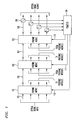
- FIG. 1 is a simplified block diagram showing an optical communication system incorporating a particular embodiment of this invention.
- three photonic modules 101, 102, and 103
- an optical signal monitor/electrical signal generator (“OSM/ESG")
- optical transmission paths 105, 106, 107, and 108 are included in the system.
- Primary information bearing optical signals travel along these optical transmission paths from input to output.
- the photonic modules within this system are each opto-electronic integrated guided-wave switching devices of the type shown in FIG. 2.
- the optical switching within such guided-wave devices is controlled by the applying voltages or currents to control electrodes internal to the devices.
- Such switching devices e.g., directional couplers
- Such switching devices are typically fabricated from lithium-niobate, and are well known in the art.
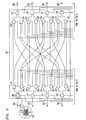
- FIG. 2 shows, in simplified form, the internal architecture of photonic module 101 of FIG. 1.
- Photonic module 101 (a 4 x 4 switch) accepts optical input signals from optical transmission paths via input lines 201, 202, 203, and 204, and outputs optical signals via lines 205-208.
- Transmission path 105 (FIG. 1) is connected to photonic module 101 via input line 201.
- a switching node having a control electrode is associated with each of the input and output lines in photonic module 101 (input nodes 209- 212 and output nodes 213-216). Additional control electrodes (217-232) are associated with the sixteen intermediate optical switching nodes within photonic module 101.
- a detailed depiction of switching node 209 (which is associated with input line 201) is shown in FIG. 2.
- a voltage applied to electrode 233 regulates the transmission of optical signals through switching node 209.
- FIG. 3 provides a graphical representation of the typical transfer characteristics for switching nodes such as those contained within photonic module 101.
- a maximum amount of light is transmitted through a switching node when the control voltage applied to that node is set to a bias point designated the "cross state" (shown as point 301 in FIG. 3).
- V o a voltage applied to that node
- V m sin(mt) a small alternating voltage
- V m sin(mt) shown as waveform 302
- the light output by the switching node is modulated accordingly (waveform 303).
- modulated output does not contain frequency components at the fundamental modulation frequency w, but rather only components at 2 ⁇ ,4 ⁇ and higher even multiples of ⁇ .
- V o- a voltage slightly less than that required to place the node at cross state bias point 301
- modulated output waveform 403 resulting from the application of voltage [Vo- + V m sin((ot)] 402 contains frequency components at the fundamental modulation frequency w, and 3 ⁇ ,5 ⁇ , etc.
- a low-frequency signal V m sin((ot) is modulated onto the optical signals traveling along optical transmission path 105 at the input of photonic module 101.
- This optical modulation is accomplished by adding a modulating voltage (generated by OSM/ESG 104 of FIG. 1) to the control voltage being applied to control electrode 233 of switching node 209 (FIG. 2).
- the frequency ⁇ is chosen so that it is well outside of the bandwidth of the primary optical signals being transmitted along optical path 105. For example, a 100 to 1000 Hz modulation frequency would be well outside the bandwidth of primary optical signals carried within an optical network capable of supporting 1 Gb/s transmissions.
- the amplitude of the modulated voltage would be kept to a minimum so as not to introduce too large a fluctuation in the level of the optical signal being modulated, thus insuring that the information carried by the primary optical signal will not be corrupted or interfered with.
- control electrode 233 causes the optical signal being transmitted along path 105, and entering photonic module 101 via input line 201 to be modulated.
- Other switching nodes within photonic module 101 are biased to allow the modulated optical signal to exit photonic module 101 at output line 205.
- the modulated signal propagates along optical transmission path 106.
- the switching nodes within photonic module 102 and photonic module 103 are biased so that the modulated signal on transmission path 106 is propagated to transmission paths 107 and 108, and to optical tap 109.
- Optical tap 109 routes a small portion of the modulated signal to OSM/ESG 104.
- OSM/ESG 104 analyzes the received optical signal and determines the frequency components of the low-frequency modulation. As the modulation is low frequency, OSM/ESG 104 may employ an inexpensive, low-speed photo-sensor arrangement to detect the signal. If the received low-frequency modulation is found to have frequency components of 2 ⁇ ,4 ⁇ ,6 ⁇ , etc., the control voltage being applied to control electrode 233 of switching node 209 is biased to enable the maximum transmission of light through node 209. However, if the received low-frequency modulation is found to have frequency components of ⁇ ,3 ⁇ ,5 ⁇ , etc., the level of the control voltage being applied to switching node 209 requires adjustment. As discussed above with respect to FIGS.
- the fundamental modulation frequency w, and odd multiples thereof, would be evident in a modulated signal only if the magnitude of control voltage applied to a particular switching node is either too great or too small.
- the phase of the fundamental modulation frequency ⁇ detected in the received optical signal with that of the electrical signal inducing the modulation, it can be determined if the magnitude of the applied control voltage is too great (phase difference of 180°), or too small (phase difference of 0°).
- the control voltage applied to the switching node at which the modulation was introduced is adjusted accordingly, and the modulation of the optical signal as it passes through the node is repeated to determine if the adjustment has placed the node at the proper cross state bias point.
- FIG. 6 is a simplified block diagram of a signal generation/detection circuit used to implement the automatic control voltage adjustment described above for switching node 209 (FIG. 2). Such a circuit is contained within OSM/ESG 104 shown in FIG. 1.
- Signal generator 601 produces a low-frequency electrical signal of frequency o) which is passed to summing element 602 and multiplier 603.
- the generated signal can be any symmetric waveform, such as a sinusoid or a saw-tooth.
- Multiplier 603 also receives an input signal from photo-detector circuit 604.
- the signal generated by photo-detector circuit 604 is proportional to the intensity of the light incident upon photodiode 605.
- This incident light is a portion of the modulated optical signal tapped from transmission path 108 by optical tap 109 (FIG. 1).
- the signal from photo-detector circuit 604 is multiplied with the low frequency signal output by signal generator 601; the product is integrated by integrator 606 and passed to summing element 602 where it is added to the output of signal generator 601.
- Integrator 606 outputs a positive voltage when the signal produced by photo-detector circuit contains a high-amplitude frequency component having the same frequency as the output of signal generator 601, but phase-shifted 180° from the output of signal generator 601.
- Integrator 606 produces a negative voltage when the signal produced by photo-detector circuit contains a high-amplitude frequency component having the same frequency and phase as the output of signal generator 601.
- integrator 606 If the signal produced by photo-detector circuit does not contain a frequency component having the same frequency as the output of signal generator 601, integrator 606 outputs a zero level signal.
- Summing element 607 adds the output of summing element 602 to a nominal control voltage being applied to switching node 209. The sum of these two signals is then applied, via control path 110 (FIG. 1), to control electrode 233 of switching node 209 (FIG. 2).
- the output of integrator 606 varies as a function of the amplitude, frequency, and phase of the signal produced by photo-detector circuit 604. This results in the output of summing element 607 providing a voltage to control electrode 233 of switching node 209 (FIG. 2) which is actively adjusted so that switching node 209 is maintained at an optimal cross state bias point.
- the monitoring and optimization technique can be applied to each of the twenty four switching nodes within photonic module 101.
- the technique may be practiced sequentially upon individual nodes, or simultaneously upon multiple nodes by employing multiple signal generation/detection circuits.
- the control voltage at each nodes is modulated at a unique frequency. Each of these unique frequencies is chosen so that one is not a multiple harmonic of another. This allows the modulated optical signal received from any particular node to be differentiated from all other received signals.
- the above described techniques may also be applied to switching nodes within photonic modules 102 and 103 (via signals scent over control paths 111 and 112, respectively).
- the monitoring and optimization scheme may also be employed in a similar fashion if the switching node is to be set in the "bar state.” In this state, light is channeled through the switching node in a direction other than the direction selected in the cross state.
- the transfer characteristic for the bar state is essentially the complement of the characteristics depicted in FIGS. 3,4, and 5. Again, the above described technique is employed to optimize the control voltage applied to the switching node for maximum transmission of light along the desired path.
- the invention provides for the practical, on-line monitoring and optimization of optical switch control parameters within an optical communication system. It will be understood that the particular methods described are only illustrative of the principles of the present invention, and that various modifications could be made by those skilled in the art without departing from the scope of the present invention.
- One such modification would include generating the electrical signals provided to the switching nodes in the above described examples at a plurality of individual electrical signal generators; each of these generators being dedicated to a particular photonic module, photonic module port, or group of photonic module ports.
Landscapes
- Engineering & Computer Science (AREA)
- Computer Networks & Wireless Communication (AREA)
- Physics & Mathematics (AREA)
- Electromagnetism (AREA)
- Signal Processing (AREA)
- Optical Communication System (AREA)
- Electronic Switches (AREA)
- Use Of Switch Circuits For Exchanges And Methods Of Control Of Multiplex Exchanges (AREA)
- Optical Modulation, Optical Deflection, Nonlinear Optics, Optical Demodulation, Optical Logic Elements (AREA)
Applications Claiming Priority (2)
| Application Number | Priority Date | Filing Date | Title |
|---|---|---|---|
| US914302 | 1992-07-17 | ||
| US07/914,302 US5317439A (en) | 1992-07-17 | 1992-07-17 | Automatic on-line monitoring and optimization of optical network switching nodes |
Publications (3)
| Publication Number | Publication Date |
|---|---|
| EP0581459A2 true EP0581459A2 (de) | 1994-02-02 |
| EP0581459A3 EP0581459A3 (de) | 1994-10-12 |
| EP0581459B1 EP0581459B1 (de) | 1998-05-27 |
Family
ID=25434162
Family Applications (1)
| Application Number | Title | Priority Date | Filing Date |
|---|---|---|---|
| EP93305289A Expired - Lifetime EP0581459B1 (de) | 1992-07-17 | 1993-07-06 | Automatische on-line-Überwachung und Optimierung von Vermittlungsknoten eines optischen Netzes |
Country Status (5)
| Country | Link |
|---|---|
| US (1) | US5317439A (de) |
| EP (1) | EP0581459B1 (de) |
| JP (1) | JP2902545B2 (de) |
| CA (1) | CA2098748C (de) |
| DE (1) | DE69318769T2 (de) |
Cited By (3)
| Publication number | Priority date | Publication date | Assignee | Title |
|---|---|---|---|---|
| WO1995020301A1 (en) * | 1994-01-25 | 1995-07-27 | Smiths Industries Aerospace & Defense Systems, Inc. | Method and apparatus for controlling an electro-optical switch |
| WO1999016192A1 (en) * | 1996-02-15 | 1999-04-01 | Honeywell, Inc. | Dual signal subharmonic carrier for systems with unknown delay |
| EP0813349A3 (de) * | 1996-06-13 | 2001-04-11 | Nortel Networks Limited | Optisches Übertragungssystem |
Families Citing this family (17)
| Publication number | Priority date | Publication date | Assignee | Title |
|---|---|---|---|---|
| US5664033A (en) * | 1994-04-05 | 1997-09-02 | Tektronix, Inc. | Remote fiber test system using a non-blocking N×N mechanical fiber optical switch |
| US5532864A (en) * | 1995-06-01 | 1996-07-02 | Ciena Corporation | Optical monitoring channel for wavelength division multiplexed optical communication system |
| US5712932A (en) * | 1995-08-08 | 1998-01-27 | Ciena Corporation | Dynamically reconfigurable WDM optical communication systems with optical routing systems |
| US5745274A (en) * | 1995-12-27 | 1998-04-28 | Lucent Technologies Inc. | Maintenance of optical networks |
| US5710846A (en) * | 1996-03-26 | 1998-01-20 | Rf Systems, Inc. | Self-calibrating optical fiber switch |
| NL1002940C2 (nl) * | 1996-04-24 | 1997-10-28 | Nederland Ptt | Optisch netwerk met protectie-configuratie. |
| JP3077600B2 (ja) * | 1996-09-26 | 2000-08-14 | 日本電気株式会社 | 光ネットワークシステムのパス監視装置 |
| JPH11122177A (ja) * | 1997-10-17 | 1999-04-30 | Fujitsu Ltd | 監視制御信号送信装置及び方法 |
| US6721508B1 (en) | 1998-12-14 | 2004-04-13 | Tellabs Operations Inc. | Optical line terminal arrangement, apparatus and methods |
| US6862380B2 (en) * | 2000-02-04 | 2005-03-01 | At&T Corp. | Transparent optical switch |
| US8363744B2 (en) | 2001-06-10 | 2013-01-29 | Aloft Media, Llc | Method and system for robust, secure, and high-efficiency voice and packet transmission over ad-hoc, mesh, and MIMO communication networks |
| AU2002228910A1 (en) * | 2000-11-03 | 2002-05-15 | Vitesse Semiconductor Corporation | Optical routers and redundancy |
| US6740864B1 (en) | 2002-04-30 | 2004-05-25 | Finisar Corporation | Method and apparatus for monitoring optical switches and cross-connects |
| US7608011B2 (en) * | 2003-01-04 | 2009-10-27 | Ford Global Technologies, Llc | Hydrogen fuelled hybrid powertrain and vehicle |
| US9567666B2 (en) * | 2009-01-12 | 2017-02-14 | Guardian Industries Corp | Apparatus and method for making sputtered films with reduced stress asymmetry |
| JP5711939B2 (ja) | 2010-11-02 | 2015-05-07 | 富士通オプティカルコンポーネンツ株式会社 | 光送信器及び光伝送装置 |
| US9819436B2 (en) | 2013-08-26 | 2017-11-14 | Coriant Operations, Inc. | Intranodal ROADM fiber management apparatuses, systems, and methods |
Family Cites Families (19)
| Publication number | Priority date | Publication date | Assignee | Title |
|---|---|---|---|---|
| US4278850A (en) * | 1978-04-11 | 1981-07-14 | Kokusai Denshin Denwa Co., Ltd. | Monitoring system for optical transmission line repeaters |
| US4301536A (en) * | 1979-12-28 | 1981-11-17 | Bell Telephone Laboratories, Incorporated | Multitone frequency response and envelope delay distortion tests |
| US4417337A (en) * | 1981-06-29 | 1983-11-22 | Bell Telephone Laboratories, Incorporated, | Adaptive multitone transmission parameter test arrangement |
| JPS58221534A (ja) * | 1982-06-18 | 1983-12-23 | Fujitsu Ltd | 光フアイバ通信方式 |
| US4649334A (en) * | 1984-10-18 | 1987-03-10 | Kabushiki Kaisha Toshiba | Method of and system for controlling a photovoltaic power system |
| US4829512A (en) * | 1986-08-26 | 1989-05-09 | Nec Corporation | Loop-back control apparatus for a loop network having duplicate optical fiber transmission lines |
| US4773071A (en) * | 1986-10-02 | 1988-09-20 | Grumman Aerospace Corporation | Memory for storing response patterns in an automatic testing instrument |
| DE3636427A1 (de) * | 1986-10-25 | 1988-05-05 | Standard Elektrik Lorenz Ag | Schaltungsanordnung und nachrichtennetzwerk mit pruefeinrichtung und pruefverfahren |
| JPS63223615A (ja) * | 1987-03-12 | 1988-09-19 | Fujitsu Ltd | 外部変調器 |
| SE458328B (sv) * | 1987-07-16 | 1989-03-13 | Ericsson Telefon Ab L M | Anordning foer fellokalisering i en dubbelriktad optisk linjelaenk |
| JPH0828680B2 (ja) * | 1987-07-23 | 1996-03-21 | 国際電信電話株式会社 | 双方向光ファイバ通信系の障害点監視方式 |
| JPS6459220A (en) * | 1987-08-31 | 1989-03-06 | Nec Corp | Optical space division matrix switch |
| US4937851A (en) * | 1988-07-20 | 1990-06-26 | Keptel, Inc. | Loop status verification system |
| US4911515A (en) * | 1988-12-22 | 1990-03-27 | Northern Telecom Limited | Optical fiber communications system with optical fiber monitoring |
| US4918396A (en) * | 1989-04-05 | 1990-04-17 | At&T Bell Laboratories | Monitoring and/or control of optical amplifiers |
| US5066118A (en) * | 1990-04-12 | 1991-11-19 | Minnesota Mining And Manufacturing Company | Optical fault finder using matched and clipping filters |
| US5069544A (en) * | 1990-04-12 | 1991-12-03 | Minnesota Mining And Manufacturing Company | Adaptive pulse width optical fault finder |
| JPH0425819A (ja) * | 1990-05-21 | 1992-01-29 | Nec Corp | 光マトリクススイッチのスイッチング状態調整方式 |
| US5218465A (en) * | 1991-09-03 | 1993-06-08 | Motorola, Inc. | Intelligent interconnects for broadband optical networking |
-
1992
- 1992-07-17 US US07/914,302 patent/US5317439A/en not_active Expired - Lifetime
-
1993
- 1993-06-18 CA CA002098748A patent/CA2098748C/en not_active Expired - Fee Related
- 1993-07-06 DE DE69318769T patent/DE69318769T2/de not_active Expired - Fee Related
- 1993-07-06 EP EP93305289A patent/EP0581459B1/de not_active Expired - Lifetime
- 1993-07-16 JP JP5197683A patent/JP2902545B2/ja not_active Expired - Fee Related
Cited By (4)
| Publication number | Priority date | Publication date | Assignee | Title |
|---|---|---|---|---|
| WO1995020301A1 (en) * | 1994-01-25 | 1995-07-27 | Smiths Industries Aerospace & Defense Systems, Inc. | Method and apparatus for controlling an electro-optical switch |
| US6075910A (en) * | 1994-01-25 | 2000-06-13 | Honeywell Inc. | Method and apparatus for controlling an electro-optical switch |
| WO1999016192A1 (en) * | 1996-02-15 | 1999-04-01 | Honeywell, Inc. | Dual signal subharmonic carrier for systems with unknown delay |
| EP0813349A3 (de) * | 1996-06-13 | 2001-04-11 | Nortel Networks Limited | Optisches Übertragungssystem |
Also Published As
| Publication number | Publication date |
|---|---|
| DE69318769D1 (de) | 1998-07-02 |
| US5317439A (en) | 1994-05-31 |
| EP0581459A3 (de) | 1994-10-12 |
| EP0581459B1 (de) | 1998-05-27 |
| CA2098748A1 (en) | 1994-01-18 |
| JP2902545B2 (ja) | 1999-06-07 |
| DE69318769T2 (de) | 1998-12-10 |
| JPH06232721A (ja) | 1994-08-19 |
| CA2098748C (en) | 1997-03-18 |
Similar Documents
| Publication | Publication Date | Title |
|---|---|---|
| US5317439A (en) | Automatic on-line monitoring and optimization of optical network switching nodes | |
| US7555226B2 (en) | Automatic bias control for an optical modulator | |
| JP5853386B2 (ja) | 光変調装置および光変調制御方法 | |
| EP0444688B1 (de) | Optischer Sender | |
| US8184355B2 (en) | Light modulation device | |
| EP2148457A2 (de) | Optischer Sender | |
| US8538263B2 (en) | Optical communication system, optical receiver of same, and optical communication method of same | |
| EP0580316B1 (de) | Funktionsüberwachung und Fehlerlokalisierung für optische Anlage, System und Netzwerk | |
| US6917455B2 (en) | Cascaded RZ and NRZ laser modulators having RZ/NRZ phase alignment bias control | |
| US20020114047A1 (en) | Cascaded RZ and NRZ laser modulators having RZ/NRZ phase alignment bias control | |
| JP4184131B2 (ja) | 光ssb変調装置 | |
| JPH0738615B2 (ja) | 光fsk周波数偏移安定化回路 | |
| US6473219B1 (en) | Method and apparatus for asymetrical optical modulation | |
| CA2182033C (en) | Method and apparatus for controlling an electro-optical switch | |
| US20040005154A1 (en) | Optical transmitter | |
| JPH05232412A (ja) | LiNbO3 マッハツェンダ干渉型変調器の制御装置 | |
| JP2757816B2 (ja) | 光強度変調器の特性測定方法及び制御方法 | |
| JP2664749B2 (ja) | 光変調装置 | |
| JPH04116618A (ja) | 光変調装置 | |
| JPH05249418A (ja) | 光変調回路 | |
| JP2869585B2 (ja) | 光変調装置 | |
| JPH0752271B2 (ja) | 光周波数安定化装置 | |
| WO2003015455A2 (en) | Optical routing apparatus | |
| JPH0856040A (ja) | 多電極レーザダイオードの波長制御装置 | |
| SE460932B (sv) | Saett att stabilisera styrningen av en elektrooptisk modulator |
Legal Events
| Date | Code | Title | Description |
|---|---|---|---|
| PUAI | Public reference made under article 153(3) epc to a published international application that has entered the european phase |
Free format text: ORIGINAL CODE: 0009012 |
|
| AK | Designated contracting states |
Kind code of ref document: A2 Designated state(s): DE FR GB |
|
| RAP3 | Party data changed (applicant data changed or rights of an application transferred) |
Owner name: AT&T CORP. |
|
| PUAL | Search report despatched |
Free format text: ORIGINAL CODE: 0009013 |
|
| AK | Designated contracting states |
Kind code of ref document: A3 Designated state(s): DE FR GB |
|
| 17P | Request for examination filed |
Effective date: 19950330 |
|
| GRAG | Despatch of communication of intention to grant |
Free format text: ORIGINAL CODE: EPIDOS AGRA |
|
| 17Q | First examination report despatched |
Effective date: 19970807 |
|
| GRAG | Despatch of communication of intention to grant |
Free format text: ORIGINAL CODE: EPIDOS AGRA |
|
| GRAH | Despatch of communication of intention to grant a patent |
Free format text: ORIGINAL CODE: EPIDOS IGRA |
|
| GRAH | Despatch of communication of intention to grant a patent |
Free format text: ORIGINAL CODE: EPIDOS IGRA |
|
| GRAA | (expected) grant |
Free format text: ORIGINAL CODE: 0009210 |
|
| AK | Designated contracting states |
Kind code of ref document: B1 Designated state(s): DE FR GB |
|
| REF | Corresponds to: |
Ref document number: 69318769 Country of ref document: DE Date of ref document: 19980702 |
|
| ET | Fr: translation filed | ||
| PLBE | No opposition filed within time limit |
Free format text: ORIGINAL CODE: 0009261 |
|
| STAA | Information on the status of an ep patent application or granted ep patent |
Free format text: STATUS: NO OPPOSITION FILED WITHIN TIME LIMIT |
|
| 26N | No opposition filed | ||
| REG | Reference to a national code |
Ref country code: GB Ref legal event code: IF02 |
|
| PGFP | Annual fee paid to national office [announced via postgrant information from national office to epo] |
Ref country code: DE Payment date: 20070719 Year of fee payment: 15 |
|
| PGFP | Annual fee paid to national office [announced via postgrant information from national office to epo] |
Ref country code: GB Payment date: 20070720 Year of fee payment: 15 |
|
| PGFP | Annual fee paid to national office [announced via postgrant information from national office to epo] |
Ref country code: FR Payment date: 20070710 Year of fee payment: 15 |
|
| GBPC | Gb: european patent ceased through non-payment of renewal fee |
Effective date: 20080706 |
|
| PG25 | Lapsed in a contracting state [announced via postgrant information from national office to epo] |
Ref country code: DE Free format text: LAPSE BECAUSE OF NON-PAYMENT OF DUE FEES Effective date: 20090203 |
|
| REG | Reference to a national code |
Ref country code: FR Ref legal event code: ST Effective date: 20090331 |
|
| PG25 | Lapsed in a contracting state [announced via postgrant information from national office to epo] |
Ref country code: GB Free format text: LAPSE BECAUSE OF NON-PAYMENT OF DUE FEES Effective date: 20080706 |
|
| PG25 | Lapsed in a contracting state [announced via postgrant information from national office to epo] |
Ref country code: FR Free format text: LAPSE BECAUSE OF NON-PAYMENT OF DUE FEES Effective date: 20080731 |