EP0584844A2 - Elément de circuit à opération multiplication-addition avec apprentissage adaptatif et circuit utilisant un élément pareil - Google Patents
Elément de circuit à opération multiplication-addition avec apprentissage adaptatif et circuit utilisant un élément pareil Download PDFInfo
- Publication number
- EP0584844A2 EP0584844A2 EP93200856A EP93200856A EP0584844A2 EP 0584844 A2 EP0584844 A2 EP 0584844A2 EP 93200856 A EP93200856 A EP 93200856A EP 93200856 A EP93200856 A EP 93200856A EP 0584844 A2 EP0584844 A2 EP 0584844A2
- Authority
- EP
- European Patent Office
- Prior art keywords
- circuit
- adaptive
- learning
- excitatory
- learning type
- Prior art date
- Legal status (The legal status is an assumption and is not a legal conclusion. Google has not performed a legal analysis and makes no representation as to the accuracy of the status listed.)
- Granted
Links
Images


Classifications
-
- H—ELECTRICITY
- H10—SEMICONDUCTOR DEVICES; ELECTRIC SOLID-STATE DEVICES NOT OTHERWISE PROVIDED FOR
- H10D—INORGANIC ELECTRIC SEMICONDUCTOR DEVICES
- H10D30/00—Field-effect transistors [FET]
-
- G—PHYSICS
- G06—COMPUTING OR CALCULATING; COUNTING
- G06N—COMPUTING ARRANGEMENTS BASED ON SPECIFIC COMPUTATIONAL MODELS
- G06N3/00—Computing arrangements based on biological models
- G06N3/02—Neural networks
- G06N3/06—Physical realisation, i.e. hardware implementation of neural networks, neurons or parts of neurons
- G06N3/063—Physical realisation, i.e. hardware implementation of neural networks, neurons or parts of neurons using electronic means
- G06N3/065—Analogue means
-
- G—PHYSICS
- G11—INFORMATION STORAGE
- G11C—STATIC STORES
- G11C11/00—Digital stores characterised by the use of particular electric or magnetic storage elements; Storage elements therefor
- G11C11/21—Digital stores characterised by the use of particular electric or magnetic storage elements; Storage elements therefor using electric elements
- G11C11/22—Digital stores characterised by the use of particular electric or magnetic storage elements; Storage elements therefor using electric elements using ferroelectric elements
-
- H—ELECTRICITY
- H03—ELECTRONIC CIRCUITRY
- H03K—PULSE TECHNIQUE
- H03K19/00—Logic circuits, i.e. having at least two inputs acting on one output; Inverting circuits
- H03K19/02—Logic circuits, i.e. having at least two inputs acting on one output; Inverting circuits using specified components
- H03K19/08—Logic circuits, i.e. having at least two inputs acting on one output; Inverting circuits using specified components using semiconductor devices
- H03K19/094—Logic circuits, i.e. having at least two inputs acting on one output; Inverting circuits using specified components using semiconductor devices using field-effect transistors
Definitions
- the present invention relates to an adaptive-learning type product-sum operation circuit element, an adaptive-learning type product-sum operation circuit and an adaptive-learning type product-sum operation circuit array for weighing and adding a number of signals input into a plurality of neuron circuits in a neural network.
- Both the methods have a problem of enormously increasing learning time in a practical network having more than 10,000 neurons.
- the present invention is to obviate the aforesaid shortcoming.
- the present invention relates to a circuit for making the weight of synaptic connection the optimum by adaptive-learning with the aid of residual polarization of a ferroelectric film, and when this circuit is used, even if the use of a network is started under such a condition that the weight of synaptic connection is not the optimum, a function of making the weight of synaptic connection the optimum as the use is progressed can be expected.
- a concrete circuit constructs a matrix of synaptic connection of m ⁇ n by connecting in parallel adaptive-learning type MISFET (metal-insulator-semiconductor field effect transistors) with the use of a ferroelectric thin film as a gate insulating film by m stages equal to a number of input signals to form synaptic connection of one neuron circuit, and further aligning the MISFETs for other neuron circuits so that n rows are formed in total.
- MISFET metal-insulator-semiconductor field effect transistors
- An object of the present invention is to provide a product-sum operation circuit comprising an insulator substrate, a single crystal semiconductor thin film having a p-n-p or n-p-n structure in a lateral direction formed in the shape of stripes on the insulator substrate, a ferroelectric thin film deposited thereon for covering at least the semiconductor stripe structure, and a strip-like electrode consisting of a metal or a polycrystalline semiconductor further formed thereon for intersecting the semiconductor stripes at a right angle or suitable angle.
- Another object of the present invention is to provide an adaptive-learning type product-sum operation circuit comprising a neuron circuit as a constituent having such an adaptive-learning function that a parallel circuit of adaptive-learning type MISFET is connected to a capacitance C in series, resistances R2 and R3 are made the other sides of a bridge and connected by a unijunction transistor (UJT), and a junction point of said MISFET and capacitance C is connected to the UJT for narrowing an interval between output pulses by a positive excitatory control signal entered into the MISFET and widening an interval between output pulses by a negative inhibitory control signal entered into the other MISFET.
- UJT unijunction transistor
- Still another object of the invention is to provide an adaptive-learning type product-sum operation circuit, comprising a photoconductor PC1 conducted by an excitatory optical information input signal and a photo-conductor PC2 conducted by an inhibitory optical information input signal connected in series between positive and negative terminals, a series circuit of a capacitance C and an adaptive-learning type FET connected between said positive and earth terminals, an LED and a series circuit of a UJT and a resistance are connected in parallel, a junction point of said photoconductor is connected to a gate electrode of said adaptive-learning type FET, an intersecting point of the adaptive-learning type FET and the capacitance C is connected to the UJT, the circuit comprising excitatory and inhibitory controls means for narrowing and widening a pulse interval of output pulses by receiving optical information input signals in PC1 and PC2, respectively.
- Yet still another object of the present invention is to provide an adaptive-learning type product-sum operation circuit comprising a series circuit of a p-channel MOSFET switch 18 conducted by an excitatory information input signal and an n-channel MOSFET switch 19 conducted by an inhibitory information input signal, a series circuit of a capacitance C and an adaptive-learning type MISFET 41, a series circuit of a resistance 26, a unijunction transister UJT 42 and a resistance R, a series circuit of a p-channel MOSFET 40 and resistances 28, 29, these circuits being connected in parallel, respectively, a junction point 20 of said FET switches 18 and 19 being connected to a gate electrode of said adaptive-learning type FET 41, a junction point 21 of said adaptive-learning type FET 41 and capacitance C being connected to said UJT 42, a junction point 27 of said UJT 42 and resistance 26 being branched from an excitatory information output terminal 24 and connected to a gate electrode of said p-channel MOSFET 40, an inhibitory information
- Yet still another object of the present invention is to provide an adaptive-learning type product-sum operation circuit array comprising an array network of neuron circuits of m ⁇ n by providing m stages of a series circuit of a photoconductor PC1 conducted by an excitatory optical information input signal, neuron circuits of n rows and a photoconductor PC2 conducted by an inhibitory optical information input signal between positive and negative terminals, excitatory control means for narrowing an interval of output pulses of each neuron circuit element by excitatory control signals, and inhibitory control means for widening an interval of output pulses of each neuron circuit element by inhibitory control signal, and further comprising adaptive-learning functions such as complement of a displaced or missing letter or pattern of input picture information.
- Yet still another object of the present invention is to provide an adaptive-learning type product-sum operation circuit array comprising an array network of neuron circuits of m ⁇ n by providing m stages of a series circuit of a semiconductor switch conducted by an excitatory electric input signal, n rows of neuron circuits and a semiconductor switch conducted by an inhibitory electric information input signal between positive and negative terminals, excitatory control means for narrowing an interval of output pulses of each neuron circuit by excitatory control signals and inhibitory control means for widening an interval of output pulses of each neuron circuit by inhibitory control signals, and further comprising adaptive-learning functions such as complement of a displaced or missing letter or pattern of an input electric information signal.
- a semiconductor stripe on an insulator substrate corresponds to a portion where metal-insulator-semiconductor field effect type transistors (MISFETs) are connected in parallel, and the uppermost metal or polycrystalline semiconductor electrode corresponds to gate electrodes of the MISFETs.
- MISFETs metal-insulator-semiconductor field effect type transistors
- This structure is characterized by enabling to give a field which can change residual polarization of a ferroelectric film only at a gate insulating film of FET of an intersecting point between a semiconductor stripe and a gate electrode stripe to where a suitable voltage is given. Therefore, when this novel characteristic is used, initial weights of every synapse can be set independently.
- 1 is a source
- 2 is a drain
- 3 is a gate
- 4 is a ferroelectric film
- 5 is a p-type (n-type) semiconductor
- C is a capacitance
- R1, R2, R3 are resistances
- 6 is an input terminal
- 7 is an output terminal
- 8 is a bias voltage terminal
- 9, 14, 30 are +V0 terminals
- 10, 15, 31 are -V0 terminals
- 11, 12 are intermediate points
- 16, 17 are input terminals
- 18, 19 are FET switches
- 20, 21, 22, 27 are intermediate points
- 13, 23 are earth terminals
- 24, 25 are output terminals, 26, 28, 29 are resistances
- 34 is an optical output portion
- 35 is an insulator substrate
- 36, 37 are Si stripes
- 38 is a ferroelectric thin film
- 39 is a gate electrode
- 40 is a p-channel MOSFET
- 41 is an adaptive-learning type MISFET
- 42 is a unijunction transistor (UJT)
- the present invention is to propose an adaptive-learning neuron circuit having a high density synapse connection consisting of a ferroelectric thin film.
- the circuit construction of the present invention will be explained by referring to the accompanying drawings in detail.
- the present inventor first observes an adaptive-learning function of an electron device and then explains the adaptive-learning type MISFET proposed by the present inventor and the principle construction of adaptive-learning function of an adaptive-learning neuron circuit with the use of the MISFET.
- the present inventors is to think that the adaptive-learning function has the following two properties.
- the functions 1 means a function for changing a normally OFF-type FET to a normally ON-type FET during a period of applying a certain number of input signals to a gate
- the function 2 means a function for generating a change of the properties under the sufficiently controlled condition, and it is different from deterioration of a device by input signals.
- a function similar to this adaptive-learning function is to apply a special control signal different from a usual signal so as to change the condition of a device.
- This function is different from the adaptive-learning function in the point of using a control signal, which is specified as a self-control function by the present inventor.
- a typical self-control device is an electrically erasable non-volatile memory (EEPROM), wherein a read-out signal corresponds to a usual signal, and a write-in signal and an erase signal correspond to special control signals.
- EEPROM electrically erasable non-volatile memory
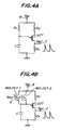
- the adaptive-learning type MISFET proposed by the present invention has the same structure as that of the usual MOSFET as shown in a schematic diagram of Fig. 1, but the point of using a ferroelectric thin film as a gate insulating film is novel.
- Fig. 1 shows an enhancement type FET of an n channel, and when a positive pulse voltage is applied to a gate, an inversion layer is formed at a channel portion in case of applying a pulse and the FET turns ON.
- polarization is generated in the ferroelectric thin film, and this polarization remains even after the voltage is back to 0, so that a conductive layer is stationarily formed on the surface of a semiconductor after several pulses are applied, and source and drain become ON even after a gate voltage is made 0. That is, the FET is changed to a normally ON-type FET by learning.
- the ferroelectric thin film requires a switching time t s for inverting spontaneous polarization P s .
- the switching time in case of applying an electric field E more than a coercive electric field E c is expressed as follow formula.
- t s t so exp (E a /E) (1)
- E a is an activation field, which value changes according to the kind of a ferroelectric material.
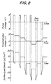
- Fig. 2 shows a calculation example of a threshold voltage of a MIS diode having a metal/ferroelectric film/Si structure and a charge density of a semiconductor surface.
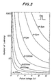
- Fig. 3 shows a relation between the learning times and a gate input voltage, where the learning times means number of input pulses until an inversion layer is formed on the initially accumulated semiconductor surface. Assumed numerical values are the same as those of Fig. 2. Fig. 3 is usable as a design chart for obtaining the thickness of a gate insulating film when learning times is designated.
- Fig. 1 is a source electrode
- 2 is a drain electrode
- 3 is a gate electrode
- 4 is a ferroelectric thin film
- 5 is a p type or n type semiconductor made of silicon (Si) and the like on an insulator substrate, and adaptive-learning effect means that the polarization of the ferroelectric thin film is gradually changed and a resistance value between the source electrode 1 and the drain electrode 2 is changed during usual signal pulses are applies to the gate electrode 3.
- Fig. 2 shows a calculation data of a threshold voltage of a MIS diode having a metal/ferroelectric film/Si structure and a charge density of a semiconductor surface.
- Fig. 3 shows a relation between a pulse voltage (V) applied to a MIS diode and a learning times, wherein "learning times" means pulse number for changing the Si surface of the MIS diode to an inversion condition. This number is changed by making the width of 1 pulse 5 ns within a range of 50 nm to 3 ⁇ m of a film thickness d of the ferroelectric thin film.
- Fig. 4 shows a fundamental circuit of a pulse generator known as a trigger circuit of thyristor.
- UJT unijunction transistor
- a pulse interval is determined by a time constant of CR1. Therefore, if a resistance R1 is replaced by a source-drain resistance of adaptive-learning FET, it becomes possible to change an output pulse interval of a neuron circuit.
- the UJT is a positive feedback type device, so that the neuron circuit is formed with an SOI (i.e Si-on-insulator) structure, and each device should electrically insulated so as not to latch up the circuit.
- Figs. 5(A) and 5(B) show one embodiment of the present invention, in which a terminal 9 is kept at a source voltage of +V0 and a terminal 10 is kept at a source voltage of -V0, between which an excitatory photoconductor PC1 and an inhibitory photoconductor PC2 are connected in series, an adaptive-learning type FET is connected to its middle point, a capacitance C is connected between the adaptive-learning type FET and the terminal 9, unijunction transistor UJT is connected to its middle point 12, a light emitting diode LED is connected to said capacitance in parallel between the terminal 9 and the unijunction transistor UJT, and a resistance R is connected between the unijunction transistor UJT and an earth terminal 13.
- Optical information input signals h ⁇ 1 and h ⁇ 2 are incident into said excitatory photoconductor PC1 and inhibitory photoconductor PC2, and an optical information output signal h ⁇ is output from LED.
- Fig. 5(B) is substitute of electric elements for the photoconductors PC1 and PC2 shown in Fig. 5(A).
- terminals 14 and 15 are kept at voltages (+V0) and (-V0), respectively, switches 18 and 19 consisting of usual MOSFET are connected to said terminals 14 and 15 for switching between source-drain electrodes by a control voltage applied to gates of terminals 16 and 17, an adaptive-learning type MISFET 41 shown in Fig.
- a capacitance C is connected between a terminal 14 and a terminal 21
- a unijunction transistor (UJT) 42 is connected to the terminal 21
- a resistance 26 is connected between terminals 14 and 22
- R is connected between the unijunction transistor (UJT) 42 and an earth terminal 23
- a p channel MOSFET 40 is connected to a middle point 27 of the terminal 22 and an output terminal 24 and an output terminal 25 divided by resistances 28 and 29 is connected to a drain terminal of the MOSFET 40.
- the other end of the resistance 29 is connected to the terminal 15.
- an excitatory information input voltage pulse is applied to the terminal 16
- an inhibitory information input voltage pulse is applied to the terminal 17
- an excitatory information output voltage pulse is output from the terminal 24, and an inhibitory information output voltage pulse is output from the terminal 25.
- Fig. 6 shows n row of neuron arrays having m stage excitatory optical input terminals and m stage inhibitory optical input terminals
- an excitatory optical information input signal is input into photo-conductors of PC1-1, PC1-2, ... PC1-m
- an inhibitory optical information input signal is input into photo-conductors of PC2-1, ... PC2-m
- a photoconductor PC1-1, n row of the gate electrodes of adaptive-learning type FETs (F1-1, F1-2, ... , F1-n) and a photoconductor PC2-1 are connected in series, other sets PC 1-m , F m-1 , F m-2 , ...
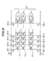
- FIG. 7 shows a circuit of a synaptic layout consisting of such adaptive-learning type FET.
- Fig. 8 shows the construction of a neuron array circuit substituting the above photoconductors PC1-1, PC1-2, ... PC1-m and PC2-1, ... , PC2-m for FET switches 45-1, 45-2, ... , 45-m and 46-1, ... , 46-m, respectively.
- Fig. 7(A) and Fig. 7(B) is a sectional view and a plan view of the circuit arrangement.
- Fig. 7(B) shows such a construction that n-p-n or p-n-p Si stripes 36 and 37 are provided on an insulator substrate 35, a ferroelectric film 38 is coated thereon, and a gate electrode 39 is further coated thereon, so as to make the Si stripes 36, 37 and gate electrode 39 a chess board cross viewed from the above.
- An adaptive-learning type neural network of the present invention was manufactured and a test was conducted for an effect thereof as follows.
- the work "adaptive-learning" can be defined as a function for changing a part or the whole of electric or optical properties of a device after the device processes a number of signals.
- an adaptive-learning neuron circuit having excitatory control means and inhibitory control means.
- the adaptive-learning device function returns to the initial value by applying an initializing signal, so that this function is different from the deterioration of the device.
- the fundamental device for carrying out the adaptive-learning function is MISFET having a ferro-electric gate insulator thin film as shown in Fig. 1.
- a pulse having a larger voltage than that of a usual signal pulse is applied to a gate electrode because the pulse having the larger voltage changes properties of a thin film.
- a thickness of the ferroelectric thin film is suitably selected for gradually changing a polarity of the thin film by applying a pulse signal.
- the normally OFF type FET where a current does not flow at a gate voltage of zero at first changes to a normally ON type FET where a current flows at a gate voltage of zero.
- the device structure can easily be designed by using switch properties of a ferroelectric thin film. An embodiment of this design is as shown in Fig. 3, and in Fig. 3, "learning times" means pulse number until the Si surface of a MIS diode changes to the inversion condition.
- the function of the adaptive-learning type MISFET gradually changes resistance between source-drain or threshold voltage when input pulse signals are applied to the gate, so that it is compatible with an analog circuit.
- a system for generating an asynchronous short interval pulse was proposed, which is similar to a current pulse generation system in human brains. This system is called PFM (pulse frequency modulation), and an interval for generating pulses has no periodicity, so that this system is different from a synchronous pulse density neural system which pulse generating time is determined.
- Fig. 4 shows a fundamental circuit of a pulse generator which is known as the trigger circuit of thyristor.
- UJT is a unijunction transistor used as a switch for discharging a capacitance C
- R1, R2 and R3 are resistances
- 7 is an output terminal
- 8 is a bias voltage terminal for charging C through R1.
- a pulse interval is determined by a time constant of CR1.
- UJT is a positive feedback type device, so that a neuron circuit is formed with an SOI (Si-on-insulator) structure, and each device should electrically be insulated so as not to latch up (i.e parasitic thyristor action) in the circuit.
- SOI Silicon-on-insulator
- FIG. 5(A) and 5(B) A circuit proposed by the present invention is as shown in Figs. 5(A) and 5(B).
- Figs. 5(A) and 5(B) there is used optical electrical coupling between neuron circuits.
- the present inventors shows a multiple input neuron circuit and a synaptically connected layout in Figs. 6 and 7.
- Fig. 6 shows n row neuron arrays having optical coupling.
- each neuron circuit has m stage synaptic connections, which are receivers of signals from respective preceding stages.
- adaptive-learning FETs of each neuron circuit are connected in parallel for determining an output pulse interval by a time constant of (capacitance C) ⁇ (total resistance R).
- Fig. 7 shows a synaptic connection layout.
- an Si stripe having a n-p-n structure in a lateral direction is arranged on an insulator substrate, and coated a ferroelectric thin film thereon, while a metal stripe for a gate electrode is arranged on the thin film at a right angle to the Si stripe.
- a +V0/2 pulse-like bias voltage and a -V0/2 direct current bias are applied to respectively selected metal and Si stripes.
- a potential difference applied to the thin film becomes V0 at only the intersection point and exceeds a critical value of polarization, and the degree of polarization, that is, the degree of weight can be controlled by varying a duration of the pulse-like bias.
- a weighting value when a weighting value is 0, it means that there is no response to input, and it also means the more the weighting value increases, the more the portion thereof is regarded as important.
- one synapse region in case of designing a circuit with a rule of the minimum width of 1 micron is about 4 ⁇ 2 ⁇ m2 (3 ⁇ m-width Si stripes, 1 ⁇ m-width metal stripes and 1 ⁇ m-width space).
- the region of each neuron circuit is not large, and the region of 1000 ⁇ 1000 synapse connections having 1,000,000 synapses is about 8 mm2. This region is considered to be sufficiently small as compared with the other neural network.
- the present inventor has found a novel adaptive-learning neuron circuit.
- the main conceptions are as follows.
- an adaptive-learning type neuron circuit in which an interval of output pulses is changed by learning by connecting a simple pulse generating circuit consisting of capacitance, resistance, unijunction transistor and the like for instance.
Landscapes
- Engineering & Computer Science (AREA)
- Physics & Mathematics (AREA)
- Health & Medical Sciences (AREA)
- Life Sciences & Earth Sciences (AREA)
- Biomedical Technology (AREA)
- Biophysics (AREA)
- Theoretical Computer Science (AREA)
- Computing Systems (AREA)
- Mathematical Physics (AREA)
- General Engineering & Computer Science (AREA)
- Neurology (AREA)
- Software Systems (AREA)
- Molecular Biology (AREA)
- Evolutionary Computation (AREA)
- Data Mining & Analysis (AREA)
- General Physics & Mathematics (AREA)
- Computational Linguistics (AREA)
- General Health & Medical Sciences (AREA)
- Artificial Intelligence (AREA)
- Computer Hardware Design (AREA)
- Power Engineering (AREA)
- Semiconductor Memories (AREA)
- Non-Volatile Memory (AREA)
- Logic Circuits (AREA)
Applications Claiming Priority (2)
| Application Number | Priority Date | Filing Date | Title |
|---|---|---|---|
| JP224111/92 | 1992-08-24 | ||
| JP4224111A JPH0731705B2 (ja) | 1992-08-24 | 1992-08-24 | 自己学習型積和演算回路素子及び回路 |
Publications (3)
| Publication Number | Publication Date |
|---|---|
| EP0584844A2 true EP0584844A2 (fr) | 1994-03-02 |
| EP0584844A3 EP0584844A3 (en) | 1994-08-24 |
| EP0584844B1 EP0584844B1 (fr) | 1998-12-23 |
Family
ID=16808711
Family Applications (1)
| Application Number | Title | Priority Date | Filing Date |
|---|---|---|---|
| EP93200856A Expired - Lifetime EP0584844B1 (fr) | 1992-08-24 | 1993-03-25 | Circuit neuronal à opération multiplication-addition avec apprentissage adaptatif |
Country Status (5)
| Country | Link |
|---|---|
| US (1) | US5519812A (fr) |
| EP (1) | EP0584844B1 (fr) |
| JP (1) | JPH0731705B2 (fr) |
| KR (1) | KR0139007B1 (fr) |
| DE (1) | DE69322712T2 (fr) |
Cited By (4)
| Publication number | Priority date | Publication date | Assignee | Title |
|---|---|---|---|---|
| EP1265254A3 (fr) * | 2001-06-06 | 2004-07-28 | Matsushita Electric Industrial Co., Ltd. | Dispositif à semi-conducteurs |
| WO2018002774A1 (fr) * | 2016-06-29 | 2018-01-04 | Semiconductor Energy Laboratory Co., Ltd. | Dispositif électronique, procédé de fonctionnement du dispositif électronique et véhicule en mouvement |
| TWI783629B (zh) * | 2020-09-11 | 2022-11-11 | 日商鎧俠股份有限公司 | 交換電路及記憶裝置 |
| US11956969B2 (en) | 2018-12-18 | 2024-04-09 | Sony Group Corporation | Semiconductor storage device using two insulative storage elements and neural network device using the same |
Families Citing this family (22)
| Publication number | Priority date | Publication date | Assignee | Title |
|---|---|---|---|---|
| US5757042A (en) * | 1996-06-14 | 1998-05-26 | Radiant Technologies, Inc. | High density ferroelectric memory with increased channel modulation and double word ferroelectric memory cell for constructing the same |
| JP2838196B2 (ja) * | 1996-08-20 | 1998-12-16 | 東京工業大学長 | 単一トランジスタ型強誘電体メモリへのデータ書込み方法 |
| US6025735A (en) * | 1996-12-23 | 2000-02-15 | Motorola, Inc. | Programmable switch matrix and method of programming |
| US5886920A (en) * | 1997-12-01 | 1999-03-23 | Motorola, Inc. | Variable conducting element and method of programming |
| US6205048B1 (en) | 1997-12-31 | 2001-03-20 | Samsung Electronics Co., Ltd. | Single transistor cell, method for manufacturing the same, memory circuit composed of single transistor cells, and method for driving the same |
| KR100261221B1 (ko) | 1997-12-31 | 2000-07-01 | 윤종용 | 단일 트랜지스터 셀 및 이를 제조하는 방법 및 이 소자로 구성된 메모리 회로와 이를 구동하는 방법 |
| KR100338552B1 (ko) | 1999-07-28 | 2002-05-27 | 윤종용 | 불휘발성 강유전체 랜덤 액세스 메모리 장치 및 그것의 데이터읽기 방법 |
| JP4252171B2 (ja) * | 1999-09-30 | 2009-04-08 | 独立行政法人科学技術振興機構 | 不揮発性メモリ |
| US7265380B2 (en) * | 2005-03-25 | 2007-09-04 | Osaka University | Ambipolar organic thin-film field-effect transistor and making method |
| CN103430186A (zh) * | 2012-01-20 | 2013-12-04 | 松下电器产业株式会社 | 神经网络电路的学习方法 |
| JP5289647B1 (ja) * | 2012-01-23 | 2013-09-11 | パナソニック株式会社 | ニューラルネットワーク回路の学習方法 |
| WO2015001697A1 (fr) * | 2013-07-04 | 2015-01-08 | パナソニックIpマネジメント株式会社 | Circuit de réseau neuronal et procédé d'apprentissage associé |
| JP5858020B2 (ja) | 2013-10-03 | 2016-02-10 | 株式会社デンソー | 群情報記憶認識装置 |
| KR102051041B1 (ko) * | 2013-10-25 | 2019-11-29 | 삼성전자주식회사 | 3단자 시냅스 소자 및 그 동작방법 |
| JP6501146B2 (ja) * | 2014-03-18 | 2019-04-17 | パナソニックIpマネジメント株式会社 | ニューラルネットワーク回路およびその学習方法 |
| US10733946B2 (en) * | 2016-08-26 | 2020-08-04 | Semiconductor Energy Laboratory Co., Ltd. | Display device and electronic device |
| US9659249B1 (en) * | 2016-09-27 | 2017-05-23 | International Business Machines Corporation | Pre-programmed resistive cross-point array for neural network |
| GB201708512D0 (en) | 2017-05-26 | 2017-07-12 | Univ Southampton | Tunable cmos circuit, template matching module, neural spike recording system, and fuzzy logic gate |
| KR20180133073A (ko) * | 2017-06-05 | 2018-12-13 | 에스케이하이닉스 주식회사 | 다수의 강유전체 전계 효과 트랜지스터들을 가진 시냅스를 포함하는 뉴로모픽 소자의 시냅스 어레이 |
| US10460817B2 (en) * | 2017-07-13 | 2019-10-29 | Qualcomm Incorporated | Multiple (multi-) level cell (MLC) non-volatile (NV) memory (NVM) matrix circuits for performing matrix computations with multi-bit input vectors |
| US10482929B2 (en) | 2017-07-13 | 2019-11-19 | Qualcomm Incorporated | Non-volative (NV) memory (NVM) matrix circuits employing NVM matrix circuits for performing matrix computations |
| CN111509040B (zh) * | 2020-04-28 | 2021-05-14 | 复旦大学 | 基于绝缘层上硅衬底的单结晶体管及其制备方法 |
Family Cites Families (10)
| Publication number | Priority date | Publication date | Assignee | Title |
|---|---|---|---|---|
| US3832700A (en) * | 1973-04-24 | 1974-08-27 | Westinghouse Electric Corp | Ferroelectric memory device |
| US4151020A (en) * | 1977-01-26 | 1979-04-24 | Texas Instruments Incorporated | High density N-channel silicon gate read only memory |
| US4184207A (en) * | 1978-01-27 | 1980-01-15 | Texas Instruments Incorporated | High density floating gate electrically programmable ROM |
| JPH0634236B2 (ja) * | 1985-11-02 | 1994-05-02 | 日本放送協会 | 階層型情報処理方法 |
| US4782460A (en) * | 1987-04-06 | 1988-11-01 | American Telephone And Telegraph Company, At&T Bell Laboratories | Computing apparatus comprising a programmable resistor |
| FR2621757A1 (fr) * | 1987-10-09 | 1989-04-14 | Thomson Csf | Reseau neuronal programmable a polymere ferroelectrique |
| JP2595051B2 (ja) * | 1988-07-01 | 1997-03-26 | 株式会社日立製作所 | 半導体集積回路 |
| US5070385A (en) * | 1989-10-20 | 1991-12-03 | Radiant Technologies | Ferroelectric non-volatile variable resistive element |
| US5065132A (en) * | 1990-11-16 | 1991-11-12 | Texas Instruments Incorporated | Programmable resistor and an array of the same |
| JP3207227B2 (ja) * | 1991-11-08 | 2001-09-10 | ローム株式会社 | 不揮発性半導体記憶装置 |
-
1992
- 1992-08-24 JP JP4224111A patent/JPH0731705B2/ja not_active Expired - Lifetime
-
1993
- 1993-03-05 US US08/026,779 patent/US5519812A/en not_active Expired - Lifetime
- 1993-03-24 KR KR1019930004555A patent/KR0139007B1/ko not_active Expired - Fee Related
- 1993-03-25 EP EP93200856A patent/EP0584844B1/fr not_active Expired - Lifetime
- 1993-03-25 DE DE69322712T patent/DE69322712T2/de not_active Expired - Fee Related
Cited By (8)
| Publication number | Priority date | Publication date | Assignee | Title |
|---|---|---|---|---|
| EP1265254A3 (fr) * | 2001-06-06 | 2004-07-28 | Matsushita Electric Industrial Co., Ltd. | Dispositif à semi-conducteurs |
| US6847071B2 (en) | 2001-06-06 | 2005-01-25 | Matsushita Electric Industrial Co., Ltd. | Semiconductor device |
| US6949780B2 (en) | 2001-06-06 | 2005-09-27 | Matsushita Electric Industrial Co., Ltd. | Semiconductor device |
| WO2018002774A1 (fr) * | 2016-06-29 | 2018-01-04 | Semiconductor Energy Laboratory Co., Ltd. | Dispositif électronique, procédé de fonctionnement du dispositif électronique et véhicule en mouvement |
| US10290266B2 (en) | 2016-06-29 | 2019-05-14 | Semiconductor Energy Laboratory Co., Ltd. | Electronic device, operation method of the electronic device, and moving vehicle |
| US11114047B2 (en) | 2016-06-29 | 2021-09-07 | Semiconductor Energy Laboratory Co., Ltd. | Electronic device, operation method of the electronic device, and moving vehicle |
| US11956969B2 (en) | 2018-12-18 | 2024-04-09 | Sony Group Corporation | Semiconductor storage device using two insulative storage elements and neural network device using the same |
| TWI783629B (zh) * | 2020-09-11 | 2022-11-11 | 日商鎧俠股份有限公司 | 交換電路及記憶裝置 |
Also Published As
| Publication number | Publication date |
|---|---|
| JPH0731705B2 (ja) | 1995-04-10 |
| EP0584844A3 (en) | 1994-08-24 |
| EP0584844B1 (fr) | 1998-12-23 |
| KR0139007B1 (ko) | 1998-06-15 |
| DE69322712D1 (de) | 1999-02-04 |
| DE69322712T2 (de) | 1999-07-22 |
| US5519812A (en) | 1996-05-21 |
| KR940004486A (ko) | 1994-03-15 |
| JPH0668288A (ja) | 1994-03-11 |
Similar Documents
| Publication | Publication Date | Title |
|---|---|---|
| EP0584844B1 (fr) | Circuit neuronal à opération multiplication-addition avec apprentissage adaptatif | |
| Hiroshi Ishiwara | Proposal of adaptive-learning neuron circuits with ferroelectric analog-memory weights | |
| US10892330B2 (en) | FET based synapse network | |
| US4873455A (en) | Programmable ferroelectric polymer neural network | |
| US5027171A (en) | Dual polarity floating gate MOS analog memory device | |
| US5055897A (en) | Semiconductor cell for neural network and the like | |
| KR100293607B1 (ko) | 신경망을갖는정보처리시스템 | |
| JP5659361B1 (ja) | ニューラルネットワーク回路、およびその学習方法 | |
| KR20190005101A (ko) | 강유전체 전계 효과 트랜지스터를 사용하는 멀티-비트, SoC-호환성 뉴로모픽 웨이트 셀 | |
| US5010512A (en) | Neural network having an associative memory that learns by example | |
| EP0566739A1 (fr) | Dispositif a semi-conducteur | |
| US6956280B2 (en) | Integrated circuit apparatus and neuro element | |
| US5264734A (en) | Difference calculating neural network utilizing switched capacitors | |
| US5818081A (en) | Semiconductor device | |
| EP0505790A2 (fr) | Synapse ionique artificielle | |
| US20200258942A1 (en) | Resistive processing units with complementary metal-oxide-semiconductor non-volatile analog memory | |
| Sun et al. | Novel a-IGZO anti-ferroelectric FET LIF neuron with co-integrated ferroelectric FET synapse for spiking neural networks | |
| JP3438241B2 (ja) | 半導体神経回路装置 | |
| Kaneko et al. | Neural network based on a three-terminal ferroelectric memristor to enable on-chip pattern recognition | |
| US20210034953A1 (en) | Reconfigurable finfet-based artificial neuron and synapse devices | |
| Borgstrom et al. | Programmable current-mode neural network for implementation in analogue MOS VLSI | |
| KR20210087389A (ko) | 신경망을 위한 시냅스 스트링 어레이 아키텍처 | |
| US5237210A (en) | Neural network accomodating parallel synaptic weight adjustments for correlation learning algorithms | |
| US12026605B2 (en) | FeFET unit cells for neuromorphic computing | |
| US5592418A (en) | Non-volatile analog memory cell with double polysilicon level |
Legal Events
| Date | Code | Title | Description |
|---|---|---|---|
| PUAI | Public reference made under article 153(3) epc to a published international application that has entered the european phase |
Free format text: ORIGINAL CODE: 0009012 |
|
| AK | Designated contracting states |
Kind code of ref document: A2 Designated state(s): DE FR GB NL |
|
| PUAL | Search report despatched |
Free format text: ORIGINAL CODE: 0009013 |
|
| AK | Designated contracting states |
Kind code of ref document: A3 Designated state(s): DE FR GB NL |
|
| 17P | Request for examination filed |
Effective date: 19950126 |
|
| 17Q | First examination report despatched |
Effective date: 19961218 |
|
| GRAG | Despatch of communication of intention to grant |
Free format text: ORIGINAL CODE: EPIDOS AGRA |
|
| GRAG | Despatch of communication of intention to grant |
Free format text: ORIGINAL CODE: EPIDOS AGRA |
|
| GRAH | Despatch of communication of intention to grant a patent |
Free format text: ORIGINAL CODE: EPIDOS IGRA |
|
| GRAH | Despatch of communication of intention to grant a patent |
Free format text: ORIGINAL CODE: EPIDOS IGRA |
|
| GRAA | (expected) grant |
Free format text: ORIGINAL CODE: 0009210 |
|
| AK | Designated contracting states |
Kind code of ref document: B1 Designated state(s): DE FR GB NL |
|
| REF | Corresponds to: |
Ref document number: 69322712 Country of ref document: DE Date of ref document: 19990204 |
|
| ET | Fr: translation filed | ||
| PLBE | No opposition filed within time limit |
Free format text: ORIGINAL CODE: 0009261 |
|
| STAA | Information on the status of an ep patent application or granted ep patent |
Free format text: STATUS: NO OPPOSITION FILED WITHIN TIME LIMIT |
|
| 26N | No opposition filed | ||
| REG | Reference to a national code |
Ref country code: GB Ref legal event code: IF02 |
|
| PGFP | Annual fee paid to national office [announced via postgrant information from national office to epo] |
Ref country code: GB Payment date: 20040130 Year of fee payment: 12 |
|
| PGFP | Annual fee paid to national office [announced via postgrant information from national office to epo] |
Ref country code: FR Payment date: 20040227 Year of fee payment: 12 |
|
| PGFP | Annual fee paid to national office [announced via postgrant information from national office to epo] |
Ref country code: NL Payment date: 20040331 Year of fee payment: 12 |
|
| PGFP | Annual fee paid to national office [announced via postgrant information from national office to epo] |
Ref country code: DE Payment date: 20040430 Year of fee payment: 12 |
|
| PG25 | Lapsed in a contracting state [announced via postgrant information from national office to epo] |
Ref country code: GB Free format text: LAPSE BECAUSE OF NON-PAYMENT OF DUE FEES Effective date: 20050325 |
|
| PG25 | Lapsed in a contracting state [announced via postgrant information from national office to epo] |
Ref country code: NL Free format text: LAPSE BECAUSE OF NON-PAYMENT OF DUE FEES Effective date: 20051001 Ref country code: DE Free format text: LAPSE BECAUSE OF NON-PAYMENT OF DUE FEES Effective date: 20051001 |
|
| GBPC | Gb: european patent ceased through non-payment of renewal fee |
Effective date: 20050325 |
|
| PG25 | Lapsed in a contracting state [announced via postgrant information from national office to epo] |
Ref country code: FR Free format text: LAPSE BECAUSE OF NON-PAYMENT OF DUE FEES Effective date: 20051130 |
|
| NLV4 | Nl: lapsed or anulled due to non-payment of the annual fee |
Effective date: 20051001 |
|
| REG | Reference to a national code |
Ref country code: FR Ref legal event code: ST Effective date: 20051130 |