EP0585619B1 - Procédé de détection de l'état nul de résultat de calculation logique ou arithmétique et circuit pour ceci - Google Patents
Procédé de détection de l'état nul de résultat de calculation logique ou arithmétique et circuit pour ceci Download PDFInfo
- Publication number
- EP0585619B1 EP0585619B1 EP93112254A EP93112254A EP0585619B1 EP 0585619 B1 EP0585619 B1 EP 0585619B1 EP 93112254 A EP93112254 A EP 93112254A EP 93112254 A EP93112254 A EP 93112254A EP 0585619 B1 EP0585619 B1 EP 0585619B1
- Authority
- EP
- European Patent Office
- Prior art keywords
- bit
- signal
- cell
- group
- operand
- Prior art date
- Legal status (The legal status is an assumption and is not a legal conclusion. Google has not performed a legal analysis and makes no representation as to the accuracy of the status listed.)
- Expired - Lifetime
Links
Images


Classifications
-
- G—PHYSICS
- G06—COMPUTING OR CALCULATING; COUNTING
- G06F—ELECTRIC DIGITAL DATA PROCESSING
- G06F7/00—Methods or arrangements for processing data by operating upon the order or content of the data handled
- G06F7/38—Methods or arrangements for performing computations using exclusively denominational number representation, e.g. using binary, ternary, decimal representation
- G06F7/48—Methods or arrangements for performing computations using exclusively denominational number representation, e.g. using binary, ternary, decimal representation using non-contact-making devices, e.g. tube, solid state device; using unspecified devices
- G06F7/50—Adding; Subtracting
- G06F7/505—Adding; Subtracting in bit-parallel fashion, i.e. having a different digit-handling circuit for each denomination
-
- G—PHYSICS
- G06—COMPUTING OR CALCULATING; COUNTING
- G06F—ELECTRIC DIGITAL DATA PROCESSING
- G06F7/00—Methods or arrangements for processing data by operating upon the order or content of the data handled
- G06F7/02—Comparing digital values
-
- G—PHYSICS
- G06—COMPUTING OR CALCULATING; COUNTING
- G06F—ELECTRIC DIGITAL DATA PROCESSING
- G06F9/00—Arrangements for program control, e.g. control units
- G06F9/06—Arrangements for program control, e.g. control units using stored programs, i.e. using an internal store of processing equipment to receive or retain programs
- G06F9/30—Arrangements for executing machine instructions, e.g. instruction decode
- G06F9/30094—Condition code generation, e.g. Carry, Zero flag
-
- G—PHYSICS
- G06—COMPUTING OR CALCULATING; COUNTING
- G06F—ELECTRIC DIGITAL DATA PROCESSING
- G06F7/00—Methods or arrangements for processing data by operating upon the order or content of the data handled
- G06F7/38—Methods or arrangements for performing computations using exclusively denominational number representation, e.g. using binary, ternary, decimal representation
- G06F7/48—Methods or arrangements for performing computations using exclusively denominational number representation, e.g. using binary, ternary, decimal representation using non-contact-making devices, e.g. tube, solid state device; using unspecified devices
- G06F7/499—Denomination or exception handling, e.g. rounding or overflow
- G06F7/49905—Exception handling
Definitions
- This invention generally relates to computer arithmetic logic units in general, and a method of detecting an arithmetic or logical computation result in particular.
- a typical computer has an arithmetic logic unit (ALU) which performs mathematical operations on two or more "N" bit operands where "N” represents the total number of bits per operand. It will also be convenient to refer to the "n"th bit where "n” is an index variable whose value is between 0 and N-1, inclusive.
- a zero detection circuit which operates to detect whether or not the result of addition/subtraction between a pair of binary numbers each composed of a plurality of bits becomes zero in all the plurality of bits is known from EP-A-0 339 685.
- the zero detection circuit comprises a plurality of condition detection circuits, which detect for each digit of the numbers A and B whether anyone of four conditions is established between a pair of bits (A i B i ) of the same digit and another pair of bits (A i+1 , B i+1 ) of a one-bit more significant digit and generate respective detection signals.
- the detection signals are supplied to a discrimination circuit, which in turn generates a discrimination output signal indicating whether or not the result is zero.
- a method as defined in claim 1 is provided.
- the present invention produces a signal for each bit, herein known as a one-bit-zero signal, of an ALU such that the arithmetic or logical condition signal may be computed independently from the computation result.
- the nth one-bit-zero signal where n is between 0 and N-1, inclusive, is preferably dependent only upon nth and n minus first (n-1)th bit of each operand.
- the least significant (zeroeth) one-bit-zero detector is dependent only on the zeroeth bit of each operand and a carry-in signal, C in , since an (n-1)th bit is not available for the least significant one-bit-zero detector.
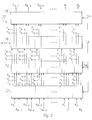
- the ALU 22 performs a specified arithmetic operation on its operands, A 0 through A N-1 and B 0 through B N-1 . These operations may be arithmetic operations such as addition or subtraction or specified logical operations such as a logical AND or logical OR.
- the preliminary ALU ⁇ 0 outputs are the outputs of OR gates 34 .
- the OR gates 34 receive the least significant bit of their associated ALU section 32 , the R ⁇ 0 signal from their associated ALU section 32 , and the ALU ⁇ 0 from an earlier section OR gate 34 , if applicable.
- the ALU ⁇ 0 ripples across the ALU through OR gates 34 as the carry signal ripples across the ALU sections 32 .
- a final comparison is made with the least significant bit of the section and the final ALU ⁇ 0 signal is generated.
- the R ⁇ 0 computation for any ALU section 32 is completed one gate delay after the ALU result for that section is completed.
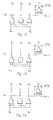
- Fig. 3 is a schematic diagram of a one-bit adder cell for prior art adders. N of these cells would be integrated with the carry-out, C n , of each cell feeding the carry-in of its next most significant neighbor. C n of the most significant (N-1st) cell would be a C out signal for use by other adders operating on yet more significant bits of an operand of greater than N bits. C n-1 of the least significant (zeroeth) cell would be a C in signal supplied from the C out signal from additional adders operating on yet less significant bits of an operand of greater than N bits.
- the circuit 40 serves to compute a one bit sum S n based on the one bit operands A n and B n , and on a carry-in signal C n-1 from a less significant one-bit cell. In the case of the least significant one-bit cell, C n-1 will be C in .
- This one-bit cell also generates two internal signals commonly referred to as the "Generate” signal, G n , and the "Propagate" signal, P n .
- the one-bit sum S n is output from another XOR gate 46 whose output is P n ⁇ C n-1 .
- the carry output C n is defined as the output of an OR gate 48 whose inputs are G n and the output of an AND gate 50 .
- the AND gate 50 receives P n and C n-1 .
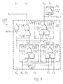
- Each of N one-bit-zero cells 62 receives inputs A n , B n and K n-1 , where n is from 0 to N-1, inclusive.
- K n is a "kill" signal which will be described below.
- Each nth one-bit-zero cell outputs a one-bit-zero signal Z n and a "kill" signal K n to be received by the next most significant (n+1) cell.
- This N-bit AND gate 64 would typically be effected by a network of gates of less than N bits in a manner obvious to one of ordinary skill in the art of digital logic circuit design.
- PGKZ Propagate, Generate, Kill, and Zero
- the one-bit-zero cell array 74 receives the PGK signals and generates a Zero signal Z n based on P n and K n-1 .
- K in for the least significant bit of the one-bit-zero array 74 K in (described below) serves as K n-1 .
- the one-bit-zero cell array 74 passes on the PGZ (Propagate, Generate, and Zero) signals.
- the combinatorial logic circuit 76 preferably an AND tree, merely passes the PG signals through, unaffected.
- the PG signals are shown passing through the on-bit-zero AND tree 76 merely for drawing convenience. No need exists for the routing of these signals to pass through or near the AND tree 76 . Still referring to Fig.
- this adder 78 may be a carry-select lookahead adder as described by Bosshart in U.S. Patent No. 4,815,019.
- it may be a ripple carry adder composed of N partial cells of Fig. 3, in which XOR gate 46 computes S n from C n-1 and P n , and OR gate 48 and AND gate 50 computes C n from P n and G n (n is from 0 to N-1, inclusive).
- the adder circuit 78 may actually perform as an arithmetic/logic circuit to generate a result for addition, subtraction, or a logical operation depending on the method used to generate P n and G n from the PGK generating unit 72 .
- the operation of adder circuit 78 is not dependent on the operation being performed.
- all operation-specific functions are performed within the PGK generating unit 72 .
- the preferred embodiment adder shown in Fig. 5 further comprises an inverter 80 for receiving a C in signal from a less significant arithmetic and logic circuit, and inverting that signal for use as K in by the PGK generating unit 72 and the one-bit-zero cell array 74 .
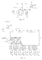
- N has been chosen to be 32 bits although N may be chosen to be any number.
- the carry tree 76 comprises a four-input AND gate 90 and four eight-input AND gates 92. As is well known in the art, these eight-input AND gates 92 could be formed from a two-input NOR gate 94 receiving the output of two four-input NAND gates 96 . Furthermore, many further functional implementations of a 32 bit AND can be accomplished by one of ordinary skill in the art.
- a first possible embodiment PGK generating circuit 72 cooperating with a possible embodiment one-bit-zero cell 74 for an adder is partially depicted.
- the embodiment of Fig. 7 is a one-bit PGKZ cell 100 for the nth bit of PGK generating circuit 72 and the nth bit of one-bit-zero cell array 74 .
- the PGKZ cell 100 comprises a first and second XOR gate 102 , 104 , an AND gate 106 , and a NOR gate 108 and inputs A n , B n , and K n-1 .
- Outputs of this PGKZ cell 100 are P n , G n , K n , and Z n .
- K in is K n-1 .
- FIG. 8 a second possible embodiment PGK generating circuit 72 cooperating with a possible embodiment one-bit-zero cell 76 for a subtracter is partially depicted.
- the embodiment of Fig. 8 is a one-bit PGKZ cell 110 for the nth bit of PGK generating circuit 72 and the nth bit of one-bit-zero cell array 74 .
- the PGKZ cell 110 comprises an XOR gate 112 , an XNOR gate 114 , a first and second NOR gate 116 , 118 , and a first and second inverter 120 , 122 .
- the PGKZ cell 110 inputs A n , B n , and K n-1 .
- Outputs of this PGKZ cell 110 are P n , G n , K n , and Z n .
- K in is K n-1 .
- FIG. 9 a third possible embodiment PGK generating circuit 72 cooperating with a possible embodiment one-bit-zero cell 76 for a general purpose ALU is partially depicted.
- the embodiment of Fig. 9 is a one-bit PGKZ cell 130 for the nth bit of PGK generating circuit 72 and the nth bit of one-bit-zero cell array 74 .
- the PGKZ cell 130 comprises an XOR gate 132 , a three input AND gate 134 , a NAND agate 136 , an OR gate 138 , a first and second inverter 140 , 142 , and a first, second, and third AND-OR-INVERT gate 144 , 146 , 148 .
- Each of the AND-OR-INVERT gates is described functionally by a NOR function 150 , and a pair of AND functions 152 .
- X n ( B n ⁇ C0 + B n ⁇ C2 )
- Y n ( B n ⁇ C1 + B n ⁇ C3 )
- K n ( ARITH ⁇ ( A n + X n ))
- G n ? ARITH ⁇ A n ⁇ X n
- Pn ( X n ⁇ A n + Y n ⁇ A n )
- Z n ? P n ⁇ K n -1
- an alternate embodiment PGK1 cell 160 of an ALU 1's circuit of an adder comprising N PGK1 cells shown schematically.
- This alternate embodiment PGK1 uses the Generate signal carried in from the next least significant bit (n-1st), in conjunction with the Propagate signal to assert a one-bit-one signal Z n '.
- This PGK1 cell 160 comprises a first and second XOR gate 162 , 164 , a NOR gate 166 , and an AND gate 168 .
- the PGK1 cell 160 inputs A n , B n , and G n-1 .
- Outputs of this PGK1 cell 160 are P n , G n , K n , and Z n '.
- G n-1 is 0.
- K n A n ⁇ B n
- G n A n ⁇ B n
- P n A n ⁇ B n
- the circuit of the preferred embodiment need only be slightly modified.
- the one-bit-zero signal is identified as P n ⁇ K n-1 .
- the zero detection in the nth bit is the XOR of bit's (bit n) propagate output with the next less significant (n-1) bit's kill output.
- the complement of the one-bit zero signal detects a one in bit n assuming bit n-1 is zero. This logic can be described by the equation P n ⁇ K n-1 .
- P n ⁇ G n-1 can be used to detect a one at bit n assuming bit n-1 is also one and P n ⁇ G n-1 detects a zero at bit n assuming bit n-1 is a one.
- bit n bit n-1 logic equation 0 0 P n ⁇ K n-1 0 1 P n ⁇ G n-1 1 0 P n ⁇ K n-1 1 1 P n ⁇ G n-1
- the logical circuit of Fig. 12 has the same or an identical PG
- the logical circuit of Fig. 13 has the same or an identical PG
- the logical circuit of Fig. 12 has the same or an identical PG
Landscapes
- Engineering & Computer Science (AREA)
- Theoretical Computer Science (AREA)
- General Physics & Mathematics (AREA)
- Physics & Mathematics (AREA)
- Mathematical Analysis (AREA)
- Pure & Applied Mathematics (AREA)
- General Engineering & Computer Science (AREA)
- Computational Mathematics (AREA)
- Mathematical Optimization (AREA)
- Software Systems (AREA)
- Computing Systems (AREA)
- Logic Circuits (AREA)
- Executing Machine-Instructions (AREA)
Claims (17)
- Procédé pour détecter si le n-ème bit du résultat d'une opération arithmétique ou logique est un ZERO logique lorsque le (n-1)-ème bit dudit résultat est un UN logique, ledit procédé ne dépendant pas du résultat calculé et comprenant les étapes consistant a :a) recevoir, au moyen d'un groupe de cellules à un bit, un premier opérande A possédant une longueur d'opérande égale à au moins deux bits;b) recevoir, au moyen dudit groupe de cellules à un bit, un second opérande B possédant une longueur d'opérande égale à au moins deux bits;c) calculer, au moyen d'une (n-1)-ème cellule dudit groupe de cellules à un bit, un signal de génération Gn-1, à partir d'un (n-1)-ème bit dudit premier opérande An-1, et à partir d'un (n-1)-ème bit dudit second opérande Bn-1, ledit signal de génération étant défini par l'équation:d) recevoir, au moyen d'une n-ème cellule dudit groupe de cellules à un bit, ledit signal de génération Gn-1; ete) calculer, au moyen de ladite n-ème cellule dudit groupe de cellules à un bit, un signal à un bit zéro Zn, à partir d'un n-ème bit dudit premier opérande An, à partir d'un n-ème bit dudit second opérande Bn et à partir dudit Gn-1, ledit signal à un bit zéro étant défini par
- Procédé selon la revendication 1 et comprenant en outre l'étape consistant à calculer, au moyen de ladite (n-1)-ème cellule dudit groupe de cellules à un bit, un signal à un bit un Zn-1', à partir dudit An-1, à partir dudit Bn-1 et à partir d'un signal de suppression Kn-2, à partir d'une (n-2)-ème cellule dudit groupe de cellules à un bit, ledit signal à un bit un étant défini par
- Procédé selon la revendication 1 et comprenant en outre l'étape consistant à calculer, au moyen de ladite (n-1)-ème cellule dudit groupe de cellules à un bit, un signal à un bit un Zn-1', à partir dudit An-1, à partir dudit Bn-1' et à partir d'un signal de génération Gn2, à partir d'une (n-2)-ème cellule dudit groupe de cellules à un bit, ledit signal à un bit un étant défini par
- Procédé pour détecter si le n-ème bit du résultat d'une opération arithmétique ou logique est un UN logique lorsque le (n-1)-ème bit dudit résultat est un ZERO logique, ledit procédé ne dépendant pas du résultat calculé et comprenant les étapes consistant à :a) recevoir, au moyen d'un groupe de cellules à un bit, un premier opérande A possédant une longueur d'opérande égale à au moins deux bits;b) recevoir, au moyen dudit groupe de cellules à un bit, un second opérande B possédant une longueur d'opérande égale à au moins deux bits;c) calculer, au moyen d'une (n-1)-ème cellule dudit groupe de cellules à un bit, un signal de suppression Kn-1, à partir d'un (n-1)-ème bit dudit premier opérande An-1, et à partir d'un (n-1)-ème bit dudit second opérande Bn-1, ledit signal de suppression étant défini par l'équation :d) recevoir, au moyen d'une n-ème cellule dudit groupe de cellules à un bit, ledit signal de suppression Kn-1; ete) calculer, au moyen de ladite n-ème cellule dudit groupe de cellules à un bit, un signal à un bit un Zn', à partir d'un n-ème bit dudit premier opérande An, à partir d'un n-ème bit dudit second opérande Bn et à partir dudit Kn-1, ledit signal à un bit un étant défini par
- Procédé selon la revendication 4 et comprenant en outre l'étape consistant à calculer, au moyen de ladite (n-1)-ème cellule dudit groupe de cellules à un bit, un signal à un bit zéro Zn-1, à partir dudit An-1, à partir dudit Bn-1, et à partir d'un signal de suppression Kn-2, à partir d'une (n-2)-ème cellule dudit groupe de cellules à un bit, ledit signal à un bit zéro étant défini par :
- Procédé selon la revendication 2 ou 5 et comprenant en outre l'étape consistant à appliquer une opération ET logique audit signal à un bit zéro et audit signal à un bit un pour générer un signal
- Procédé selon la revendication 4 et comprenant en outre l'étape consistant à calculer, au moyen de ladite (n-1)-ème cellule dudit groupe de cellules à un bit, un signal à un bit zéro Zn-1, à partir dudit An-1 et à partir dudit Bn-1 et à partir d'un signal de génération Gn-2, a partir d'une (n-2)-ème cellule dudit groupe de cellules à un bit, ledit signal à un bit un étant défini par :
- Procédé selon la revendication 3 ou 7 et comprenant en outre l'étape consistant à appliquer une combinaison ET logique audit signal à un bit zéro et audit signal à un bit un pour produire un signal
- Procédé selon la revendication 4, selon lequel n = 0 et Kn-1 est l'inverse logique du report entrant dans ledit groupe de cellules à un bit.
- Procédé de détection si le n-ème bit du résultat d'une opération arithmétique ou logique est un UN logique lorsque le (n-1)-ème bit dudit résultat est un UN logique, ledit procédé ne dépendant pas du résultat calculé et comprenant les étapes consistant à :a) recevoir, au moyen d'un groupe de cellules à un bit, un premier opérande A possédant une longueur d'opérande égale à au moins deux bits;b) recevoir, au moyen dudit groupe de cellules à un bit, un second opérande B possédant une longueur d'opérande égale à au moins deux bits;c) calculer, au moyen d'une (n-1)-ème cellule dudit groupe de cellules à un bit, un signal de génération Gn-1, a partir d'un (n-1)-ème bit dudit premier opérande An-1, et à partir d'un (n-1)-ème bit dudit second opérande Bn-1, ledit signal de génération étant défini par l'équation :d) recevoir, au moyen d'une n-ème cellule dudit groupe de cellules à un bit, ledit signal de génération Gn-1; ete) calculer, au moyen de ladite n-ème cellule dudit groupe de cellules à un bit, un signal à un bit un Zn', à partir d'un n-ème bit dudit premier opérande An, à partir d'un n-ème bit dudit second opérande Bn et à partir dudit Gn-1, ledit signal à un bit un étant défini par
- Procédé selon la revendication 10 et comprenant en outre l'étape consistant à calculer, par ladite (n-1)-ème cellule dudit groupe de cellules à un bit, un signal à un bit zéro Zn-1' à partir dudit An-1, à partir dudit Bn-1 et à partir d'un signal de suppression Kn-2, a partir d'une (n-2)-ème cellule dudit groupe de cellules à un bit, ledit signal à un bit un étant défini par
- Procédé selon la revendication 11 et comprenant l'étape consistant à appliquer une combinaison ET logique audit signal à un bit un Zn' et audit signal à un bit un Zn-1' pour produire un signal
- Procédé selon la revendication 10 et comprenant en outre l'étape consistant à calculer, au moyen de ladite (n-1)-ème cellule dudit groupe de cellules à un bit, un signal à un bit zéro Zn-1', à partir dudit An-1 et à partir dudit Bn-1 et à partir d'un signal de génération Gn-2, a partir d'une (n-2)-ème cellule dudit groupe de cellules à un bit, ledit signal à un bit un étant défini par
- Procédé selon la revendication 13 et comprenant en outre l'étape consistant à appliquer une combinaison ET logique audit signal à un bit un Zn' et audit signal à un bit un Zn-1' pour produire un signal
- Procédé selon la revendication 1 ou 10, selon lequel n = 0 et Gn-1 est le report entrant dans ledit groupe de cellules à un bit.
- Procédé selon la revendication 1, 4 ou 10, selon lequel ledit groupe de cellules à un bit reçoit un premier opérande A0 = AN-1', possédant une longueur de N bits.
- Procédé selon la revendication 1, 4 ou 10, selon lequel ledit groupe de cellules à un bit reçoit un second opérande B0 - BN-1, possédant une longueur de N bits.
Applications Claiming Priority (2)
| Application Number | Priority Date | Filing Date | Title |
|---|---|---|---|
| US922926 | 1992-07-31 | ||
| US07/922,926 US5270955A (en) | 1992-07-31 | 1992-07-31 | Method of detecting arithmetic or logical computation result |
Publications (3)
| Publication Number | Publication Date |
|---|---|
| EP0585619A2 EP0585619A2 (fr) | 1994-03-09 |
| EP0585619A3 EP0585619A3 (en) | 1994-08-10 |
| EP0585619B1 true EP0585619B1 (fr) | 2000-03-08 |
Family
ID=25447805
Family Applications (1)
| Application Number | Title | Priority Date | Filing Date |
|---|---|---|---|
| EP93112254A Expired - Lifetime EP0585619B1 (fr) | 1992-07-31 | 1993-07-30 | Procédé de détection de l'état nul de résultat de calculation logique ou arithmétique et circuit pour ceci |
Country Status (4)
| Country | Link |
|---|---|
| US (3) | US5270955A (fr) |
| EP (1) | EP0585619B1 (fr) |
| JP (1) | JP3560623B2 (fr) |
| DE (1) | DE69327996T2 (fr) |
Families Citing this family (35)
| Publication number | Priority date | Publication date | Assignee | Title |
|---|---|---|---|---|
| US5469377A (en) * | 1992-08-18 | 1995-11-21 | Nec Corporation | Floating point computing device for simplifying procedures accompanying addition or subtraction by detecting whether all of the bits of the digits of the mantissa are 0 or 1 |
| US5598514A (en) * | 1993-08-09 | 1997-01-28 | C-Cube Microsystems | Structure and method for a multistandard video encoder/decoder |
| US5487025A (en) * | 1993-11-15 | 1996-01-23 | Intergraph Corporation | Carry chain adder using regenerative push-pull differential logic |
| US5367477A (en) * | 1993-11-29 | 1994-11-22 | Motorola, Inc. | Method and apparatus for performing parallel zero detection in a data processing system |
| GB9404377D0 (en) * | 1994-03-07 | 1994-04-20 | Texas Instruments Ltd | Improvements in or relating to a comparator scheme |
| US5638312A (en) * | 1995-03-03 | 1997-06-10 | Hal Computer Systems, Inc. | Method and apparatus for generating a zero bit status flag in a microprocessor |
| US5910909A (en) * | 1995-08-28 | 1999-06-08 | C-Cube Microsystems, Inc. | Non-linear digital filters for interlaced video signals and method thereof |
| US5978826A (en) * | 1995-12-01 | 1999-11-02 | Lucent Techologies Inc. | Adder with even/odd 1-bit adder cells |
| US5798958A (en) * | 1996-06-05 | 1998-08-25 | Samsung Electronics Co., Ltd. | Zero detect for binary sum |
| US5875121A (en) * | 1996-08-06 | 1999-02-23 | Hewlett-Packard Company | Register selection system and method |
| US6018757A (en) * | 1996-08-08 | 2000-01-25 | Samsung Electronics Company, Ltd. | Zero detect for binary difference |
| US6161164A (en) * | 1996-09-16 | 2000-12-12 | International Business Machines Corp. | Content addressable memory accessed by the sum of two operands |
| US6114945A (en) * | 1997-05-08 | 2000-09-05 | Texas Instruments Incorporated | Apparatus and method for programmable fast comparison of a result of a logic operation with an selected result |
| US5975749A (en) * | 1997-07-11 | 1999-11-02 | International Business Machines Corporation | Zero and one detection chain for a carry select adder |
| US5978825A (en) * | 1997-11-14 | 1999-11-02 | Crystal Semiconductor Corp. | Zero detection circuitry and methods |
| US6272514B1 (en) * | 1997-11-18 | 2001-08-07 | Intrinsity, Inc. | Method and apparatus for interruption of carry propagation on partition boundaries |
| US6301600B1 (en) * | 1997-11-18 | 2001-10-09 | Intrinsity, Inc. | Method and apparatus for dynamic partitionable saturating adder/subtractor |
| US6269387B1 (en) * | 1997-12-11 | 2001-07-31 | Intrinsity, Inc. | Method and apparatus for 3-stage 32-bit adder/subtractor |
| US6088763A (en) * | 1998-03-16 | 2000-07-11 | International Business Machines Corporation | Method and apparatus for translating an effective address to a real address within a cache memory |
| FR2776407B1 (fr) * | 1998-03-20 | 2001-06-08 | Gemplus Card Int | Systeme et procede pour realiser des fonctions particulieres dans des etiquettes sans contact |
| US6065969A (en) | 1998-08-10 | 2000-05-23 | Mattel, Inc. | Computer game for designing and printing nail coverings |
| US6963965B1 (en) | 1999-11-30 | 2005-11-08 | Texas Instruments Incorporated | Instruction-programmable processor with instruction loop cache |
| US7231414B1 (en) * | 2000-02-09 | 2007-06-12 | Hewlett-Packard Development Company, L.P. | Apparatus and method for performing addition of PKG recoded numbers |
| US6539413B1 (en) * | 2000-03-15 | 2003-03-25 | Agere Systems Inc. | Prefix tree adder with efficient sum generation |
| US7028069B1 (en) * | 2000-05-01 | 2006-04-11 | Raza Microelectronics Inc. | Dynamic circuit using exclusive states |
| US6598066B1 (en) * | 2000-05-23 | 2003-07-22 | Sun Microsystems, Inc. | Fast carry-out generation |
| US6912560B2 (en) * | 2000-12-08 | 2005-06-28 | Agere Systems, Inc. | Adder with improved overflow flag generation |
| US7290027B2 (en) * | 2002-01-30 | 2007-10-30 | International Business Machines Corporation | Circuit suitable for use in a carry lookahead adder |
| US7739324B1 (en) | 2006-03-22 | 2010-06-15 | Cadence Design Systems, Inc. | Timing driven synthesis of sum-of-product functional blocks |
| US8707225B1 (en) | 2006-04-07 | 2014-04-22 | Cadence Design Systems, Inc. | Synthesis of area-efficient subtractor and divider functional blocks |
| US8015230B2 (en) * | 2007-06-08 | 2011-09-06 | Apple Inc. | Fast modular zero sum and ones sum determination |
| RU2420868C1 (ru) * | 2009-10-02 | 2011-06-10 | Лев Петрович Петренко | СПОСОБ ФОРМИРОВАНИЯ ПРЕОБРАЗОВАННЫХ АРГУМЕНТОВ АНАЛОГОВЫХ СИГНАЛОВ (0j)i и (0j+1)i СКВОЗНОГО ПАРАЛЛЕЛЬНОГО ПЕРЕНОСА f(←←) ДЛЯ ПРЕОБРАЗОВАНИЯ ПОЗИЦИОННО-ЗНАКОВЫХ АРГУМЕНТОВ АНАЛОГОВЫХ СИГНАЛОВ ±[nj]f(+/-) В УСЛОВНОЙ "i" ЗОНЕ МИНИМИЗАЦИИ И ФУНКЦИОНАЛЬНАЯ СТРУКТУРА ДЛЯ ЕГО РЕАЛИЗАЦИИ (ВАРИАНТЫ) |
| RU2420869C1 (ru) * | 2009-10-05 | 2011-06-10 | Лев Петрович Петренко | СПОСОБ ФОРМИРОВАНИЯ СКВОЗНОГО ПОСЛЕДОВАТЕЛЬНОГО ПЕРЕНОСА В ПРОЦЕДУРЕ ЛОГИЧЕСКОГО ДИФФЕРЕНЦИРОВАНИЯ d/dn ПОЗИЦИОННЫХ АРГУМЕНТОВ [mj]f(2n) С УЧЕТОМ ИХ ЗНАКА ДЛЯ ФОРМИРОВАНИЯ ПОЗИЦИОННО-ЗНАКОВОЙ СТРУКТУРЫ ±[mj]f(+/-)min С МИНИМИЗИРОВАННЫМ ЧИСЛОМ АКТИВНЫХ В НЕЙ АРГУМЕНТОВ (ВАРИАНТЫ) |
| RU2424550C1 (ru) * | 2010-03-04 | 2011-07-20 | Лев Петрович Петренко | ФУНКЦИОНАЛЬНАЯ СТРУКТУРА ПОСЛЕДОВАТЕЛЬНЫХ СКВОЗНЫХ ПЕРЕНОСОВ fj+1(←←)+ и fj(←←)+ УСЛОВНО "I" "ЗОНЫ ФОРМИРОВАНИЯ" ДЛЯ КОРРЕКТИРОВКИ РЕЗУЛЬТИРУЮЩЕЙ СУММЫ ПРЕДВАРИТЕЛЬНОГО СУММИРОВАНИЯ АКТИВНЫХ АРГУМЕНТОВ МНОЖИМОГО [mj]f(2n) ПОЗИЦИОННОГО ФОРМАТА В ПАРАЛЛЕЛЬНО-ПОСЛЕДОВАТЕЛЬНОМ УМНОЖИТЕЛЕ fΣ(Σ) (ВАРИАНТЫ) |
| RU2445680C1 (ru) * | 2010-11-03 | 2012-03-20 | Лев Петрович Петренко | ФУНКЦИОНАЛЬНАЯ СТРУКТУРА СКВОЗНОГО ПЕРЕНОСА f1(←←)i+1 И f2(←←)i УСЛОВНО "i+1" И УСЛОВНО "i" РАЗРЯДОВ "k" ГРУППЫ АРГУМЕНТОВ МНОЖИМОГО [ni]f(2n) ПРЕДВАРИТЕЛЬНОГО СУММАТОРА fΣ([ni]&[ni,0]) ПАРАЛЛЕЛЬНО-ПОСЛЕДОВАТЕЛЬНОГО УМНОЖИТЕЛЯ fΣ(Σ) (ВАРИАНТЫ) |
Family Cites Families (8)
| Publication number | Priority date | Publication date | Assignee | Title |
|---|---|---|---|---|
| US3983382A (en) * | 1975-06-02 | 1976-09-28 | International Business Machines Corporation | Adder with fast detection of sum equal to zeroes or radix minus one |
| US4764887A (en) * | 1985-08-02 | 1988-08-16 | Advanced Micro Devices, Inc. | Carry-bypass arithmetic logic unit |
| JP2610417B2 (ja) * | 1985-12-23 | 1997-05-14 | 日本テキサス・インスツルメンツ株式会社 | アドレス信号生成方法及びその回路 |
| US4815019A (en) * | 1987-02-26 | 1989-03-21 | Texas Instruments Incorporated | Fast ALU equals zero circuit |
| US4924422A (en) * | 1988-02-17 | 1990-05-08 | International Business Machines Corporation | Method and apparatus for modified carry-save determination of arithmetic/logic zero results |
| JPH01277931A (ja) * | 1988-04-29 | 1989-11-08 | Nec Ic Microcomput Syst Ltd | 零検出回路 |
| US4926369A (en) * | 1988-10-07 | 1990-05-15 | International Business Machines Corporation | Leading 0/1 anticipator (LZA) |
| US5095458A (en) * | 1990-04-02 | 1992-03-10 | Advanced Micro Devices, Inc. | Radix 4 carry lookahead tree and redundant cell therefor |
-
1992
- 1992-07-31 US US07/922,926 patent/US5270955A/en not_active Expired - Lifetime
-
1993
- 1993-07-30 EP EP93112254A patent/EP0585619B1/fr not_active Expired - Lifetime
- 1993-07-30 JP JP19059893A patent/JP3560623B2/ja not_active Expired - Fee Related
- 1993-07-30 DE DE69327996T patent/DE69327996T2/de not_active Expired - Fee Related
- 1993-12-13 US US08/166,370 patent/US5508950A/en not_active Expired - Lifetime
-
1995
- 1995-06-07 US US08/478,145 patent/US5600583A/en not_active Expired - Lifetime
Also Published As
| Publication number | Publication date |
|---|---|
| EP0585619A3 (en) | 1994-08-10 |
| JP3560623B2 (ja) | 2004-09-02 |
| US5600583A (en) | 1997-02-04 |
| US5508950A (en) | 1996-04-16 |
| EP0585619A2 (fr) | 1994-03-09 |
| DE69327996T2 (de) | 2000-10-26 |
| DE69327996D1 (de) | 2000-04-13 |
| JPH06348454A (ja) | 1994-12-22 |
| US5270955A (en) | 1993-12-14 |
Similar Documents
| Publication | Publication Date | Title |
|---|---|---|
| EP0585619B1 (fr) | Procédé de détection de l'état nul de résultat de calculation logique ou arithmétique et circuit pour ceci | |
| US7395304B2 (en) | Method and apparatus for performing single-cycle addition or subtraction and comparison in redundant form arithmetic | |
| US5317527A (en) | Leading one/zero bit detector for floating point operation | |
| US4924422A (en) | Method and apparatus for modified carry-save determination of arithmetic/logic zero results | |
| US4320464A (en) | Binary divider with carry-save adders | |
| US6018757A (en) | Zero detect for binary difference | |
| US8370415B2 (en) | Overflow detection and clamping with parallel operand processing for fixed-point multipliers | |
| US4618956A (en) | Method of operating enhanced alu test hardware | |
| US5579254A (en) | Fast static CMOS adder | |
| US5790444A (en) | Fast alignment unit for multiply-add floating point unit | |
| US5671171A (en) | Shared rounding hardware for multiplier and divider/square root unit using conditional sum adder | |
| US6499044B1 (en) | Leading zero/one anticipator for floating point | |
| CA2078319C (fr) | Methode et dispositif de generation de signaux de controle | |
| US5867413A (en) | Fast method of floating-point multiplication and accumulation | |
| JP2554452B2 (ja) | 自己検査型補数加算器ユニット | |
| US7139789B2 (en) | Adder increment circuit | |
| US6629118B1 (en) | Zero result prediction | |
| US5235539A (en) | Method and apparatus for generating carry out signals | |
| US5150319A (en) | Circuitry for rounding in a floating point multiplier | |
| US7206802B2 (en) | Hybrid carry look ahead/carry select adder including carry logic generating complementary hot carry signals, and method for producing the carry logic | |
| JPH09114641A (ja) | 最上位デジットを決定するための装置と方法 | |
| US5798958A (en) | Zero detect for binary sum | |
| US5635858A (en) | Zero-stopping incrementers | |
| US6826588B2 (en) | Method and apparatus for a fast comparison in redundant form arithmetic | |
| US6470373B1 (en) | Sum interval detector |
Legal Events
| Date | Code | Title | Description |
|---|---|---|---|
| PUAI | Public reference made under article 153(3) epc to a published international application that has entered the european phase |
Free format text: ORIGINAL CODE: 0009012 |
|
| AK | Designated contracting states |
Kind code of ref document: A2 Designated state(s): DE FR GB IT NL |
|
| PUAL | Search report despatched |
Free format text: ORIGINAL CODE: 0009013 |
|
| AK | Designated contracting states |
Kind code of ref document: A3 Designated state(s): DE FR GB IT NL |
|
| 17P | Request for examination filed |
Effective date: 19950112 |
|
| 17Q | First examination report despatched |
Effective date: 19980417 |
|
| GRAG | Despatch of communication of intention to grant |
Free format text: ORIGINAL CODE: EPIDOS AGRA |
|
| GRAG | Despatch of communication of intention to grant |
Free format text: ORIGINAL CODE: EPIDOS AGRA |
|
| GRAH | Despatch of communication of intention to grant a patent |
Free format text: ORIGINAL CODE: EPIDOS IGRA |
|
| GRAH | Despatch of communication of intention to grant a patent |
Free format text: ORIGINAL CODE: EPIDOS IGRA |
|
| GRAA | (expected) grant |
Free format text: ORIGINAL CODE: 0009210 |
|
| ITF | It: translation for a ep patent filed | ||
| AK | Designated contracting states |
Kind code of ref document: B1 Designated state(s): DE FR GB IT NL |
|
| REF | Corresponds to: |
Ref document number: 69327996 Country of ref document: DE Date of ref document: 20000413 |
|
| ET | Fr: translation filed | ||
| PLBE | No opposition filed within time limit |
Free format text: ORIGINAL CODE: 0009261 |
|
| 26N | No opposition filed | ||
| REG | Reference to a national code |
Ref country code: GB Ref legal event code: IF02 |
|
| PGFP | Annual fee paid to national office [announced via postgrant information from national office to epo] |
Ref country code: DE Payment date: 20080731 Year of fee payment: 16 |
|
| PGFP | Annual fee paid to national office [announced via postgrant information from national office to epo] |
Ref country code: NL Payment date: 20080619 Year of fee payment: 16 Ref country code: IT Payment date: 20080717 Year of fee payment: 16 Ref country code: FR Payment date: 20080707 Year of fee payment: 16 |
|
| PGFP | Annual fee paid to national office [announced via postgrant information from national office to epo] |
Ref country code: GB Payment date: 20080616 Year of fee payment: 16 |
|
| GBPC | Gb: european patent ceased through non-payment of renewal fee |
Effective date: 20090730 |
|
| NLV4 | Nl: lapsed or anulled due to non-payment of the annual fee |
Effective date: 20100201 |
|
| REG | Reference to a national code |
Ref country code: FR Ref legal event code: ST Effective date: 20100331 |
|
| PG25 | Lapsed in a contracting state [announced via postgrant information from national office to epo] |
Ref country code: FR Free format text: LAPSE BECAUSE OF NON-PAYMENT OF DUE FEES Effective date: 20090731 |
|
| PG25 | Lapsed in a contracting state [announced via postgrant information from national office to epo] |
Ref country code: GB Free format text: LAPSE BECAUSE OF NON-PAYMENT OF DUE FEES Effective date: 20090730 |
|
| PG25 | Lapsed in a contracting state [announced via postgrant information from national office to epo] |
Ref country code: DE Free format text: LAPSE BECAUSE OF NON-PAYMENT OF DUE FEES Effective date: 20100202 |
|
| PG25 | Lapsed in a contracting state [announced via postgrant information from national office to epo] |
Ref country code: IT Free format text: LAPSE BECAUSE OF NON-PAYMENT OF DUE FEES Effective date: 20090730 |
|
| PG25 | Lapsed in a contracting state [announced via postgrant information from national office to epo] |
Ref country code: NL Free format text: LAPSE BECAUSE OF NON-PAYMENT OF DUE FEES Effective date: 20100201 |