EP0586860A2 - Composition pour photoréserve et procédé pour obtenir des structures avec ce matériel - Google Patents
Composition pour photoréserve et procédé pour obtenir des structures avec ce matériel Download PDFInfo
- Publication number
- EP0586860A2 EP0586860A2 EP19930112105 EP93112105A EP0586860A2 EP 0586860 A2 EP0586860 A2 EP 0586860A2 EP 19930112105 EP19930112105 EP 19930112105 EP 93112105 A EP93112105 A EP 93112105A EP 0586860 A2 EP0586860 A2 EP 0586860A2
- Authority
- EP
- European Patent Office
- Prior art keywords
- photoresist composition
- resist
- resist layer
- based resin
- silylated
- Prior art date
- Legal status (The legal status is an assumption and is not a legal conclusion. Google has not performed a legal analysis and makes no representation as to the accuracy of the status listed.)
- Withdrawn
Links
Images



Classifications
-
- G—PHYSICS
- G03—PHOTOGRAPHY; CINEMATOGRAPHY; ANALOGOUS TECHNIQUES USING WAVES OTHER THAN OPTICAL WAVES; ELECTROGRAPHY; HOLOGRAPHY
- G03F—PHOTOMECHANICAL PRODUCTION OF TEXTURED OR PATTERNED SURFACES, e.g. FOR PRINTING, FOR PROCESSING OF SEMICONDUCTOR DEVICES; MATERIALS THEREFOR; ORIGINALS THEREFOR; APPARATUS SPECIALLY ADAPTED THEREFOR
- G03F7/00—Photomechanical, e.g. photolithographic, production of textured or patterned surfaces, e.g. printing surfaces; Materials therefor, e.g. comprising photoresists; Apparatus specially adapted therefor
- G03F7/004—Photosensitive materials
-
- G—PHYSICS
- G03—PHOTOGRAPHY; CINEMATOGRAPHY; ANALOGOUS TECHNIQUES USING WAVES OTHER THAN OPTICAL WAVES; ELECTROGRAPHY; HOLOGRAPHY
- G03F—PHOTOMECHANICAL PRODUCTION OF TEXTURED OR PATTERNED SURFACES, e.g. FOR PRINTING, FOR PROCESSING OF SEMICONDUCTOR DEVICES; MATERIALS THEREFOR; ORIGINALS THEREFOR; APPARATUS SPECIALLY ADAPTED THEREFOR
- G03F7/00—Photomechanical, e.g. photolithographic, production of textured or patterned surfaces, e.g. printing surfaces; Materials therefor, e.g. comprising photoresists; Apparatus specially adapted therefor
- G03F7/004—Photosensitive materials
- G03F7/022—Quinonediazides
- G03F7/023—Macromolecular quinonediazides; Macromolecular additives, e.g. binders
- G03F7/0233—Macromolecular quinonediazides; Macromolecular additives, e.g. binders characterised by the polymeric binders or the macromolecular additives other than the macromolecular quinonediazides
-
- G—PHYSICS
- G03—PHOTOGRAPHY; CINEMATOGRAPHY; ANALOGOUS TECHNIQUES USING WAVES OTHER THAN OPTICAL WAVES; ELECTROGRAPHY; HOLOGRAPHY
- G03F—PHOTOMECHANICAL PRODUCTION OF TEXTURED OR PATTERNED SURFACES, e.g. FOR PRINTING, FOR PROCESSING OF SEMICONDUCTOR DEVICES; MATERIALS THEREFOR; ORIGINALS THEREFOR; APPARATUS SPECIALLY ADAPTED THEREFOR
- G03F7/00—Photomechanical, e.g. photolithographic, production of textured or patterned surfaces, e.g. printing surfaces; Materials therefor, e.g. comprising photoresists; Apparatus specially adapted therefor
- G03F7/004—Photosensitive materials
- G03F7/0045—Photosensitive materials with organic non-macromolecular light-sensitive compounds not otherwise provided for, e.g. dissolution inhibitors
-
- G—PHYSICS
- G03—PHOTOGRAPHY; CINEMATOGRAPHY; ANALOGOUS TECHNIQUES USING WAVES OTHER THAN OPTICAL WAVES; ELECTROGRAPHY; HOLOGRAPHY
- G03F—PHOTOMECHANICAL PRODUCTION OF TEXTURED OR PATTERNED SURFACES, e.g. FOR PRINTING, FOR PROCESSING OF SEMICONDUCTOR DEVICES; MATERIALS THEREFOR; ORIGINALS THEREFOR; APPARATUS SPECIALLY ADAPTED THEREFOR
- G03F7/00—Photomechanical, e.g. photolithographic, production of textured or patterned surfaces, e.g. printing surfaces; Materials therefor, e.g. comprising photoresists; Apparatus specially adapted therefor
- G03F7/26—Processing photosensitive materials; Apparatus therefor
Definitions
- the present invention relates to a photoresist composition and process for forming a pattern using the same, and particularly to a photoresist composition including two different kinds of resins and a process for forming a pattern using the same.
- the lithography process includes the steps of coating a resist on the surface of a wafer substrate, selectively exposing the coated resist to ultraviolet rays, electron rays or X-rays and then developing the exposure.
- the remaining resist protects the substrate which the resist covers, while various additive or substractive process are performed on the exposed substrate.
- the resolution a planner substrate is determined by the exposure contrast and the lithographic contrast of the resist. Accordingly, in order to manufacture micron and sub-micron patterns with high resolution, high-contrast resists and a good exposing apparatus should be used. In such a case, the difference of the exposure dosage which is in accordance with the light absorbance of the resist owing to the difference of the resist thickness, and the inherent factors of optical lithography such as the reflectance from the substrate, the light scattering, etc. become the factors which lower the resolution. Besides the problem of resolution, heat stability and resistance against dry etching are necessary as a masking characteristic and the resist should have a thickness of at least 1 am.
- a multi-layer resist process has been proposed and, here, the use of a tri-layer resist structure achieved good results.
- this multi-layer process also has problems in that the process is complicated, a film and an inter-layer are liable to receive stress during a baking step. Also, forming a thin and even resist without pin holes via coating is difficult.
- double-layer system including silicon-containing resist has been developed.
- more than 10% of silicon should be contained in the resist, which deteriorates physical and chemical properties of the resists. Therefore, the double-layer system is rarely used nowadays.
- a diffusion-enhanced silylated resist (DESIRE) process which includes both the functionality of the multi-layer and the simplicity of the single layer, has been proposed and is being regarded as a preferable solution (see F. Coopmans and B. Roland. Solid State Technology, June 1987, pp 93-99).
- Silylation is a process whereby silicon is incorporated into a resist polymer by exposing the material to a gaseous or liquid-silicon-containing compound, such as hexamethyldisilazane (HMDS) or Tetramethyldisilazane(TMDS), at a high temperature (100-200 ° C).
- HMDS hexamethyldisilazane
- TMDS Tetramethyldisilazane
- a resist layer 2 is formed by coating a novolac-based photoresist resin on a wafer 1.
- resist layer 2 is exposed to ultraviolet rays 4 using a photo mask 3 on which a mask pattern is formed.
- resist layer 2 is divided into an exposed portion 6 and an unexposed portion 5.
- the photosensitive compound in exposed portion 6 of resist layer 2 dissociates so that -OH groups of molecules in the resist resin become free (FIG.1).
- resist layer 2 is baked at a temperature above 140 ° C (FIG.2). Through this baking, the resin particles in unexposed portion 5 of resist layer 2 cross-links with the photosensitive compound to form a polymer layer 7. This process is called a pre-silylation bake (or PSB) process.
- PSB pre-silylation bake
- silicon-containing compounds such as HMDS or tetramethyldisilazane (TMDS) is introduced over the resist layer in a gaseous state.
- TMDS tetramethyldisilazane
- the resin particles in exposed portion 6 of resist layer 2 selectively react with silicon in the HMDS or TMDS to form a silylated resist layer 9. This is called a silylation process (FIG.3).
- the resist layer is dry-developed using oxygen plasma to form a resist pattern (FIG.4).
- the silicon in silylated resist layer 9 rapidly combines with oxygen to form a silicon dioxide layer which acts as a barrier. Therefore, the resist under silylated resist layer 9 is not removed, while the other portion of the resist is removed to form a resist pattern.
- the dry development is generally carried out by reactive-ion-etching (RIE) and is otherwise called resist etching.
- RIE reactive-ion-etching
- Performing the above fundamental four steps of coating-exposing-silylation-developing produces a relief image having a negative tone.
- the process for forming a relief image having a negative tone using the novolac-based photoresist is called a negative tone process.
- the negative relief image obtained through the negative tone process can be formed using a chemical amplification resist containing a cross-linking agent.
- a cross-linked polymer layer is formed on the exposed portion of the resist layer and a silylation layer is formed on the surface of the resist of the unexposed portion.
- the reversed relief image is obtained. This is known as a positive tone process.
- a process for generating the above-mentioned positive tone photoresist in an oxygen plasma is disclosed in U.S. Patent No. 4,657,845.
- a polymer containing a masked reactive functionality is coated on a substrate, and then exposed to radiation.
- the polymer is processed in an imagewise manner to unmask selected portions of the reactive functionality.
- the polymer is treated with a non-organometallic reagent which reacts with the unmasked reactive functionality to remask that functionality.
- the resist is treated with organometallic reagents containing an element which forms a non-volatile oxide, and developed by means of oxygen reactive-ion-etching.
- organometallic species silicon compounds such as hexamethyldisilazane. N,N-dimethylaminotrimethylsilane etc., or a tin compound is used.
- a positive tone functional photoresist in order to form a positive tone resist pattern, a positive tone functional photoresist should be used and complicated processes such as alkaline treatment, flood exposure, etc. are necessary.
- a new chemical amplification resist system which has an enhanced photosensitivity to ultraviolet radiation (200-300nm).
- a photosensitive acid generator hereinafter referred to as a "PAG” decomposes and initially produces an acid. Then, an acid-catalyzed heat reaction occurs, to thereby render the exposed portion of the resist soluble in the case of positive resists, and insoluble in the case of negative resists.
- the acid-labile dissolution controlling material is known as a dissolution inhibitor.
- examples thereof include bisphenol-A protected with tetrahydropyranyl group (THP-BA), bisphenol-A protected with tert-butoxycarbonyl group (tBOC-BA), bisphenol-A protected with trimethylsilyl group (TMS-BA), the above-mentioned THP-M, etc.
- Patterns having a size of 0.3 ⁇ m may be formed by using the above photoresist composition.
- the packaging density of a semiconductor device increases, patterns smaller than 0.3 ⁇ m because necessary, especially for 64Mb and 256Mb DRAMs.
- resist patterns below 0.3 ⁇ m are not easy to form by the above conventional process.
- the conventional photoresist composition comprises, as a main component, a single polymer for both positive tone and negative tone processes, reactivity differs according to pattern sizes, and therefore, not only could the linearity not be obtained for patterns smaller than 0.30tim, but also simultaneous formation of both patterns smaller than 0.30tim and larger than 0.50tim was difficult.
- the present inventors have discovered that using a resist composition prepared by mixing resists having different silylating reactivies, uniformly controls the silylation reaction and produces patterns having good linearity in spite of varying sizes.
- the present invention has been accomplished as a result of this discovery.
- an object of the present invention is to provide a photoresist composition which can produce resist patterns having sizes smaller than 0.3 ⁇ m and having a good linearity using the DESIRE process or the conventional developing process.
- Another object of the present invention is to provide a process for forming a pattern using the above-mentioned photoresist composition.
- a photoresist composition comprising a novolac-based resin having the following structure A and a polyvinylphenol-based resin having the following structure B: wherein R 11 represents hydrogen or C 1-6 alkyl group, R 1 represents C 1-6 alkylene group, and ni and n 2 represent positive integers.
- a process for photoresist patterning comprising the steps of: coating on the semiconductor wafer to form a resist layer with a photoresist composition including novolac-based resin having the following structure A, and polyvinyl phenol- based resin having the following structure B: wherein R11 represents hydrogen or C, - 6 alkyl group, R 12 represents C, - 6 alkylene, and ni and n 2 represent positive integers; selectively exposing the resist layer using a photo mask; selectively silylating a portion of the resist layer to form a silylated resist layer on the surface of the resist layer; and removing the un-silylated resist layer, while leaving resist under the silylated resist layer.
- a photoresist composition including novolac-based resin having the following structure A, and polyvinyl phenol- based resin having the following structure B: wherein R11 represents hydrogen or C, - 6 alkyl group, R 12 represents C, - 6 alkylene, and ni and n 2 represent
- optimization of the silylation process is performed prior to the developing process by properly mixing more than two kinds of resins having different molecular structures and different molecular weights.
- a 0.25 ⁇ m-sized pattern having a good profile can be obtained.
- the linearity between pattern sizes is maintained satisfactorily to the pattern size of 0.25 ⁇ m. Therefore, patterns having sizes of 0.25 ⁇ m and larger can be simultaneously obtained.
- the novolac-based resin and the polyvinylphenol-based resin are known as being used as photoresists.
- the conventional photoresist comprises a single resin as a main component.
- the molecules of the photoresist resin should contain therein a functional group such as -OH.
- This functional group reacts with a silylating agent to selectively form a silylated resist layer on the surface of the resist layer during the above silylation.
- the silylated resist layer plays the role of an etching mask when forming a photoresist pattern by a dry etching using 0 2 plasma.
- the silylation factors include the used reagents such as a photosensitive agent (for example, the PAG), silylation agent, etc. and the type and structure of photoresist.
- the reaction process is optimized by properly mixing more than two kinds of resins having different molecular structures and different molecular weights. That is, resins having higher silylation reactivity and counterpart resins having lower silylation reactivity than a predetermined (or ideal) value are effectively selected and mixed.
- the reactivity of the resins are dependent on the type of resins used and the silylating agent.
- the quantities of the compounds are determined by comparing the relative yields after silylation, by means of a spectrometer such as an FT-IR.
- the numerical values of the silylation reactivity are determined by quantizing the relative variation of the Si-H or Si-O, and Si-C peaks after silylation of the resist by means of the above spectrometer.
- the photoresist composition of the present invention comprises, as a main component, a novolac-based resin having the following structure A and a polyvinylphenol-based resin having the following structure B: wherein R11 represents hydrogen or C, - 6 alkyl, R 12 represents C, - 6 alkylene, and n i and n 2 represent positive integers.
- the mixing ratio of the novolac-based resin and the polyvinylphenol-based resin ranges from 9:1 to 1:9 by weight. If the mixing ratio is beyond the above range, the obtained resist patterns are worse than the patterns formed using the single resins.
- the weight-average molecular weight of the novolac-based resin preferably ranges from about 1,000 to 30,000 and the weight-average molecular weight of the polyvinylphenol-based resin preferably ranges from about 2,000 to 150,000.
- the photoresist composition of the present invention may further include additives according to a process for forming a pattern, i.e. whether it is a positive or negative tone process.
- the photoresist composition of the present invention may include a PAG compound and cross-linking agents.
- PAG compound which can be used in the present invention, onium salts, DDT, S-triazine derivatives, nitrobenzyl sulfonate, and aryl or alkyl sulfonic acid esters of phenol derivatives may be included. Among these, 1,2,3-tris(methanesulfonyloxy)benzene is preferably employed.
- the added amount of the PAG compound is preferably not more than 10% by weight, more preferably from 3 to 7% by weight, and most preferably, 5% by weight, based on the total weight of the photoresist composition comprised of the novolac-based resin and the polyvinylphenol-based resin.
- cross-linking agent which can be used in the present invention, melamine or benzyl alcohol derivatives may be included.
- the added amount of the cross-linking agent preferably ranges from 10 to 30% by weight, and more preferably, 15% by weight, based on the total weight of the photoresist composition comprised of the novolac-based resin and the polyvinylphenol-based resin.
- the photoresist composition of the present invention may include a photoactive compound (PAC) or both a PAG compound and a dissolution inhibitor (which are mentioned above).
- PAC photoactive compound
- examples of the PAC include diazonaphtoquinones and others.
- the process for forming a photoresist pattern comprises the steps of: coating the above-mentioned photoresist composition on a semiconductor substrate to form a resist layer, selectively exposing the resist layer to a radiation, silylating an exposed portion of the resist layer to form a silylated resist layer on the surface portion of the resist layer, and then removing a portion of the un-silylated resist layer, while leaving the resist under the silylated resist layer.
- the process of the present invention can be carried out by a negative tone process in which an exposed portion of the resist layer is selectively silylated, or by a positive tone process in which an unexposed portion of the resist layer is selectively silylated.
- the removing step of the un-silylated portion of the resist excluding the resist under the silylated resist layer can be carried out by a one-step process using 0 2 plasma or by a two-step process comprising the steps of partially etching the un-silylated resist and silylated resist using a CF 4 and 0 2 system during a first stage, and then etching using 0 2 plasma during a second stage.
- the resist near the patterns tends to be parasitically exposed owing to light diffraction.
- the parasitically exposed resists are silylated during silylation and act as an etching mask during the resist etching step, and accordingly produce a bad profile during resist etching, and after the resist etching, produce a residue between the patterns, which adversely affects a subsequent process.
- a two-step process of the removing of the un-silylated resist is preferably carried out by etching about from 10nm to 30nm of both the silylated and un-silylated resist layer using CF 4 and 0 2 plasma during a first stage, and then etching the resultant using 0 2 plasma during a second stage.
- Another process for forming a photoresist pattern comprises the steps of: coating the above photoresist composition on the semiconductor substrate to form a resist layer, selectively exposing the resist layer using a photo mask, developing the exposed resist layer to form a resist pattern.
- the photoresist composition may further include the PAG compound and cross-linking agent in the case of forming the resist pattern by the negative tone process.
- the photoresist composition may further include the PAC or both the PAG compound and the dissolution inhibitor in the case of forming the resist pattern by the positive tone process.
- the amounts of the above-mentioned additives are the same as described above.
- a mixture solution containing 1.5 to 3wt% of tetramethyl ammonium hydroxide (TMAH) in deionized water can be used.
- a photoresist composition was prepared by mixing novolac-based resin having a weight-average molecular weight of about 5,000 with polyvinylphenol resin having a weight-average molecular weight of about 40,000 at the mixing ratio of 3:1 by weight. To the composition, 5% by weight of tris-(methanesulfonyloxy)benzene as a PAG compound and 15% by weight of melamine as a cross-linking agent based on the total weight of the thus-obtained photoresist composition were added to obtain the photoresist composition including the additives.
- the resist patterns of the present invention using the thus-obtained photoresist composition including the additives were formed as follows.
- a photoresist solution was prepared by dissolving the above-obtained photoresist composition in diethyleneglycol dimethyl ether as a solvent.
- the resist solution was spin-coated on a semiconductor wafer to a thickness of about 1 ⁇ m and then soft-baked at a temperature of about 90 ° C for one minute, to thereby give a photoresist layer.
- the photoresist layer was selectively exposed using a photo mask having respective line widths of 0.25tim, 0.30tim, 0.35tim and 0.40 ⁇ m according to a design rule and using a KrF excimer laser stepper with a numerical aperture of 0.45.
- the exposed photoresist layer was silylated using TMDS as a silylating agent at a temperature of about 100 ° C. Then, the -OH in the resin reacted with the silylating agent to transform -Ph-O-Si-(Me) 2 H. This reaction can be detected by using the FT-IR.
- the resist layer was developed using an 0 2 plasma resist etching apparatus model BMC-600 (manufactured by MRC Co.) which employs a magnetic-enhanced reactive-ion-etching (MERIE) method, in the same manner as described in the aforementioned U.S. patent (No. 4,657,845), to thereby form photoresist patterns.
- BMC-600 manufactured by MRC Co.
- MIE magnetic-enhanced reactive-ion-etching
- the unexposed surface portion of the resist layer became silylated resist layer, and was more etching-resistant to the 0 2 plasma treatment when compared to the exposed cross-linked photoresist. That is, in the 0 2 plasma treating, the silylated resist layer transformed into SiO x which is etching-resistant to the 0 2 plasma etching and remained as patterns after the 0 2 plasma treatment and the un-silylated exposed resist was removed by 0 2 plasma, to thereby form a positive tone pattern.
- FIG.5 to FIG.8 are SEM pictures of resist patterns manufactured by Example 1. As can be seen from the SEM pictures, when forming the resist patterns by using the photoresist composition of the present invention. 0.25am-, 0.30am-, 0.35 ⁇ m- and 0.40 ⁇ m-sized patterns having good profiles were obtained.
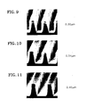
- Positive tone photoresist patterns having 0.30 ⁇ m, 0.34 ⁇ m and 0.40 ⁇ m sizes were formed by following the same procedure as described in Example 1, except that the photoresist composition prepared by mixing the novolac-based resin with the polyvinylphenol resin at a mixing ratio of 1:4 instead of 3:1 was used.
- FIG.9 to FIG.11 are SEM pictures of resist patterns manufactured by Example 2. As can be seen from the SEM pictures, 0.30 ⁇ m-, 0.34 ⁇ m- and 0.40 ⁇ m-sized patterns having good profiles were formed by using the photoresist composition of the present invention.
- a photoresist layer was formed on a semiconductor wafer using the same photoresist composition employed in Example 1 in the same manner as in Example 1.
- the resist layer was exposed with a photo mask and then developed using as a developer a mixed solution containing 1.5 to 3wt% of TMAH in deionized water, to form a negative tone photoresist patterns.
- the pattern profile was observed through an electron microscope and was found that resist patterns having profiles the same as those formed in Example 1 were formed.
- a photoresist layer was formed on a semiconductor wafer in the same procedure as in Example 1, except that a photoresist composition containing 20% by weight of a diazonaphtoquinone (based on the resin mixture) as a PAC was employed instead of using the PAG compound and cross-linking agent.
- a positive tone photoresist patterns were formed by exposing the resist layer by means of a photo mask and then developing with a mixed solution (as a developer) containing 1.5 to 3% by weight of TMAH in deionized water.
- the pattern profile was observed through an electron microscope and was found that resist patterns having profiles the same as those formed in Example 1 were formed.
- Positive tone photoresist patterns were formed in the same manner as in Example 1, except that, first, the un-silylated resist layer and silylated resist layer were etched using fifteen SCCM of CF 4 and fifteen SCCM of 0 2 to a thickness of about 10nm to 20nm for fifteen seconds during a first stage and then the resist under the un-silylated resist layer was etched using 0 2 plasma during a second stage, instead of etching the un-silylated exposed resist using 0 2 plasma.
- the parasitically silylated resist formed in the parasitically exposed resist which was formed during the resist layer exposure was removed at the first etching stage. It was found that the resist patterns obtained in this example had better and more clear profiles than those obtained in Example 1 wherein a one-step etching was performed.
- FIG.12 is a graph representing the observed size of the patterns obtained according to a process of the present invention using the photoresist composition of the present invention with respect to the designed size of the pattern.
- the abscissa represents the designed size of the patterns and the ordinate represents the observed size of the patterns. From this graph, it is noted that the linearity between the pattern sizes is maintained satisfactorily to the pattern size of 0.25tim.
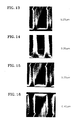
- Photoresist patterns were formed by following the same procedure as described in Example 1, except that a photoresist composition was prepared by mixing the novolac-based resin having a molecular weight of about 5,000 with the polyvinylphenol resin having a molecular weight of about 40,000 at a ration of 10:1 instead of 3:1.
- FIGs.13 to 16 are SEM pictures of resist patterns manufactured in this comparative example. Patterns of 0.25tim and 0.30 ⁇ m were difficult to form. Also, the etching procedure was disturbed by the resist residues between the patterns, and pattern profiles of 0.35 ⁇ m and 0.40 ⁇ m were less than desirable, as can be seen from the pictures.
- Resist patterns were formed by following the same procedure described in Example 1 except that using a photoresist composition prepared using a single resin which is either novolac-based resin having a molecular weight of about 5,000 or a polyvinylphenol resin having a molecular weight of 40,000.
Landscapes
- Physics & Mathematics (AREA)
- General Physics & Mathematics (AREA)
- Spectroscopy & Molecular Physics (AREA)
- Materials For Photolithography (AREA)
- Photosensitive Polymer And Photoresist Processing (AREA)
- Exposure And Positioning Against Photoresist Photosensitive Materials (AREA)
Applications Claiming Priority (2)
| Application Number | Priority Date | Filing Date | Title |
|---|---|---|---|
| KR1019920016548A KR950004908B1 (ko) | 1992-09-09 | 1992-09-09 | 포토 레지스트 조성물 및 이를 이용한 패턴형성방법 |
| KR1654892 | 1992-09-09 |
Publications (2)
| Publication Number | Publication Date |
|---|---|
| EP0586860A2 true EP0586860A2 (fr) | 1994-03-16 |
| EP0586860A3 EP0586860A3 (en) | 1994-05-18 |
Family
ID=19339377
Family Applications (1)
| Application Number | Title | Priority Date | Filing Date |
|---|---|---|---|
| EP19930112105 Withdrawn EP0586860A3 (en) | 1992-09-09 | 1993-07-29 | Photoresist composition and process for forming a pattern using the same |
Country Status (4)
| Country | Link |
|---|---|
| EP (1) | EP0586860A3 (fr) |
| JP (1) | JPH06194836A (fr) |
| KR (1) | KR950004908B1 (fr) |
| CN (1) | CN1083938A (fr) |
Cited By (3)
| Publication number | Priority date | Publication date | Assignee | Title |
|---|---|---|---|---|
| WO1997034197A1 (fr) * | 1996-03-11 | 1997-09-18 | Hoechst Celanese Corporation | Compositions de resine destinees a des applications utilisant des photoresines |
| EP0855620A1 (fr) * | 1997-01-27 | 1998-07-29 | JSR Corporation | Composition de photoréserver travaillant en positif |
| US6828079B2 (en) | 2001-09-06 | 2004-12-07 | Sumitomo Chemical Company, Limited | Chemical amplification type positive resist composition |
Families Citing this family (9)
| Publication number | Priority date | Publication date | Assignee | Title |
|---|---|---|---|---|
| KR100245410B1 (ko) * | 1997-12-02 | 2000-03-02 | 윤종용 | 감광성 폴리머 및 그것을 이용한 화학증폭형 레지스트 조성물 |
| KR100557606B1 (ko) * | 1999-08-31 | 2006-03-10 | 주식회사 하이닉스반도체 | 유기 난반사 방지용 중합체 |
| JP3874989B2 (ja) * | 2000-03-21 | 2007-01-31 | シャープ株式会社 | パターンの形成方法 |
| KR100533362B1 (ko) * | 2000-04-19 | 2005-12-06 | 주식회사 하이닉스반도체 | 레지스트 플로우 공정용 포토레지스트 조성물 및 이를이용한 콘택홀의 형성방법 |
| KR101240643B1 (ko) * | 2005-07-08 | 2013-03-08 | 삼성디스플레이 주식회사 | 포토레지스트 조성물, 상기 포토레지스트 조성물을 이용한 패턴의 형성 방법 및 이를 이용한 박막 트랜지스터표시판의 제조 방법 |
| CN102478762B (zh) * | 2010-11-24 | 2014-02-26 | 中芯国际集成电路制造(上海)有限公司 | 光刻方法 |
| KR20130072954A (ko) * | 2011-12-22 | 2013-07-02 | 제일모직주식회사 | 컬러필터용 감광성 수지 조성물 및 이를 이용한 컬러필터 |
| CN103035512B (zh) * | 2012-11-02 | 2015-08-19 | 上海华虹宏力半导体制造有限公司 | 一种非感光性聚酰亚胺钝化层的制作方法 |
| TWI753105B (zh) * | 2017-02-22 | 2022-01-21 | 日商信越化學工業股份有限公司 | 圖型形成方法 |
Family Cites Families (6)
| Publication number | Priority date | Publication date | Assignee | Title |
|---|---|---|---|---|
| GB1375461A (fr) * | 1972-05-05 | 1974-11-27 | ||
| JPS58205147A (ja) * | 1982-05-25 | 1983-11-30 | Sumitomo Chem Co Ltd | ポジ型フオトレジスト組成物 |
| JPS60154248A (ja) * | 1984-01-24 | 1985-08-13 | Japan Synthetic Rubber Co Ltd | ポジ型感光性樹脂組成物 |
| US4657845A (en) * | 1986-01-14 | 1987-04-14 | International Business Machines Corporation | Positive tone oxygen plasma developable photoresist |
| JPS6452139A (en) * | 1987-05-18 | 1989-02-28 | Konishiroku Photo Ind | Photosensitive composition |
| CA2000710A1 (fr) * | 1988-10-21 | 1990-04-21 | Richard Vicari | Copolymeres de 4-vinylphenol et de derives alkyles du 4-vinylphenol |
-
1992
- 1992-09-09 KR KR1019920016548A patent/KR950004908B1/ko not_active Expired - Fee Related
-
1993
- 1993-07-29 EP EP19930112105 patent/EP0586860A3/en not_active Withdrawn
- 1993-08-04 JP JP5193551A patent/JPH06194836A/ja active Pending
- 1993-09-09 CN CN93117375A patent/CN1083938A/zh active Pending
Cited By (4)
| Publication number | Priority date | Publication date | Assignee | Title |
|---|---|---|---|---|
| WO1997034197A1 (fr) * | 1996-03-11 | 1997-09-18 | Hoechst Celanese Corporation | Compositions de resine destinees a des applications utilisant des photoresines |
| EP0855620A1 (fr) * | 1997-01-27 | 1998-07-29 | JSR Corporation | Composition de photoréserver travaillant en positif |
| US5942369A (en) * | 1997-01-27 | 1999-08-24 | Jsr Corporation | Positive photoresist composition |
| US6828079B2 (en) | 2001-09-06 | 2004-12-07 | Sumitomo Chemical Company, Limited | Chemical amplification type positive resist composition |
Also Published As
| Publication number | Publication date |
|---|---|
| KR940007608A (ko) | 1994-04-27 |
| JPH06194836A (ja) | 1994-07-15 |
| EP0586860A3 (en) | 1994-05-18 |
| CN1083938A (zh) | 1994-03-16 |
| KR950004908B1 (ko) | 1995-05-15 |
Similar Documents
| Publication | Publication Date | Title |
|---|---|---|
| TWI476816B (zh) | 自我對準間隔之多重圖案化方法 | |
| CN102074462B (zh) | 形成电子器件的方法 | |
| KR940004423B1 (ko) | 포토래지스트층에서 네거티브 패턴을 형성하는 방법 | |
| CN101963754B (zh) | 形成电子器件的方法 | |
| KR100480611B1 (ko) | 기상 실릴레이션을 이용한 반도체 소자의 미세 패턴 형성방법 | |
| JP3835545B2 (ja) | フォトレジストパターンの形成方法及び半導体素子の製造方法 | |
| EP0187295B1 (fr) | Procédé photolithographique | |
| US20150185620A1 (en) | Photoresist pattern trimming compositions and methods | |
| US20060160028A1 (en) | Method of forming fine patterns of a semiconductor device | |
| EP0860740B1 (fr) | Matériau pour la formation de modèles très fins | |
| US6730458B1 (en) | Method for forming fine patterns through effective glass transition temperature reduction | |
| EP0586860A2 (fr) | Composition pour photoréserve et procédé pour obtenir des structures avec ce matériel | |
| JP2004505319A (ja) | 微細電子デバイスの製造方法 | |
| JPH11186243A (ja) | 酸化シリコン層のエッチング方法 | |
| EP0274757A2 (fr) | Procédé lithographique à deux couches | |
| WO1999052018A1 (fr) | Procede microlithographique a couche mince de formation d'images a l'aide de rayons dans des longueurs d'onde a forte attenuation | |
| US20050112497A1 (en) | Organic anti-reflective coating composition and method for forming photoresist pattern using the same | |
| EP1208408A1 (fr) | Materiau de revetement anti-reflet pour photoresists | |
| EP1578855A1 (fr) | Composition antireflet a partie inferieure organique et procede de formation de motifs faisant appel a ladite composition | |
| EP0199303A2 (fr) | Procédé pour obtenir des structures formant un agent de photoréserve | |
| US6989227B2 (en) | E-beam curable resist and process for e-beam curing the resist | |
| US6815367B2 (en) | Elimination of resist footing on tera hardmask | |
| Goethals et al. | Reduction of lateral swelling and incoporation of DESIRE in MOS processing | |
| US20240377744A1 (en) | Local shadow masking for multi-color exposures | |
| US6841338B2 (en) | Photoresist composition and method of forming a photoresist pattern with a controlled remnant ratio |
Legal Events
| Date | Code | Title | Description |
|---|---|---|---|
| PUAI | Public reference made under article 153(3) epc to a published international application that has entered the european phase |
Free format text: ORIGINAL CODE: 0009012 |
|
| AK | Designated contracting states |
Kind code of ref document: A2 Designated state(s): DE FR GB IT NL |
|
| RIN1 | Information on inventor provided before grant (corrected) |
Inventor name: HAN, WOO-SUNG Inventor name: LEE, JOONG-HYUN Inventor name: PARK, CHUN-GEUN |
|
| PUAL | Search report despatched |
Free format text: ORIGINAL CODE: 0009013 |
|
| AK | Designated contracting states |
Kind code of ref document: A3 Designated state(s): DE FR GB IT NL |
|
| 17P | Request for examination filed |
Effective date: 19941103 |
|
| 17Q | First examination report despatched |
Effective date: 19970509 |
|
| STAA | Information on the status of an ep patent application or granted ep patent |
Free format text: STATUS: THE APPLICATION IS DEEMED TO BE WITHDRAWN |
|
| 18D | Application deemed to be withdrawn |
Effective date: 19970922 |