EP0588700A1 - Lesegeschützter Programmspeicher - Google Patents
Lesegeschützter Programmspeicher Download PDFInfo
- Publication number
- EP0588700A1 EP0588700A1 EP93402217A EP93402217A EP0588700A1 EP 0588700 A1 EP0588700 A1 EP 0588700A1 EP 93402217 A EP93402217 A EP 93402217A EP 93402217 A EP93402217 A EP 93402217A EP 0588700 A1 EP0588700 A1 EP 0588700A1
- Authority
- EP
- European Patent Office
- Prior art keywords
- memory
- encryption
- transistors
- bit line
- same
- Prior art date
- Legal status (The legal status is an assumption and is not a legal conclusion. Google has not performed a legal analysis and makes no representation as to the accuracy of the status listed.)
- Granted
Links
Images



Classifications
-
- G—PHYSICS
- G11—INFORMATION STORAGE
- G11C—STATIC STORES
- G11C7/00—Arrangements for writing information into, or reading information out from, a digital store
- G11C7/10—Input/output [I/O] data interface arrangements, e.g. I/O data control circuits, I/O data buffers
- G11C7/1006—Data managing, e.g. manipulating data before writing or reading out, data bus switches or control circuits therefor
-
- G—PHYSICS
- G11—INFORMATION STORAGE
- G11C—STATIC STORES
- G11C7/00—Arrangements for writing information into, or reading information out from, a digital store
- G11C7/24—Memory cell safety or protection circuits, e.g. arrangements for preventing inadvertent reading or writing; Status cells; Test cells
Definitions
- the present invention relates to a semiconductor program memory protected in read mode.
- Semiconductor program memories of the read only memory type, are currently widely used, because of their reliability and their level of integration of the corresponding circuits.
- FIG. 1a a semiconductor memory device of the conventional read-only memory type is shown, constituted by N-type transistors for example, these transistors, denoted T ij, being arranged and addressed in matrix form in rows and columns .
- the number of memory points, at the level of which a logical variable can be memorized, is the product mxn of the number of rows m by the number of columns n.
- the gates of the transistors of the same line are electrically connected to a word line, WL1 to WL4, and the transistors of the same column are connected to a bit line, BL1 to BL4, polarized in the high state, level logic 1.
- the programming of the memory points then consists in isolating these transistors from the bit line according to the desired logic level, 1 or 0. This operation is carried out at a specific manufacturing level, generally metal level.
- a transistor N located on a selected word line by read addressing, causes the discharge of the bit line in the low state, logic level 0, if the drain of this transistor is connected to this bit line , the source thereof being connected to the supply voltage Vss.
- FIG. 1b a memory device is shown in which the transistors N of the same column are interconnected in series, so that only one of them is connected to a bit line. All the N transistors of the same line have their gate connected to a line of word and all word lines are polarized high, logic value 1, except that which is selected, by read addressing. A transistor N whose gate is connected to the aforementioned line goes into the blocked state, which prohibits the discharge of the bit line, and therefore determines a programming level 1.
- the programming of a programming level 0 is obtained by short-circuiting the drain and source at the metal level, or by depleting this transistor, so as to allow the discharge of the bit line.
- FIG. 1c represents a memory device derived from the device represented in FIG. 1b, and in which several columns are connected to the same bit line by transistors N for access or selection, denoted T is , controlled by lines of selection SEL1 to SEL4, so that only one of these columns is connected to the aforementioned bit line. All the access transistors of the same line have their gate connected to the same selection line, the storage transistors being denoted T isj .
- the object of the present invention is to remedy the aforementioned drawback, in order to eliminate any risk of reading by external direct access, to the memory programs and to the stored data.
- Another object of the present invention is also the implementation of a protection system for external reading of a semiconductor program memory, of the read only memory type, totally indistinguishable by visual or optical observation of the storage circuits properly speaking. said.
- Another object of the present invention is finally the implementation of a protection system for external reading of a semiconductor program memory, of read-only memory type, by encryption, by which any external access for successful reading. unauthorized requires both knowledge of the content of the encryption data and of the matrix arrangement of the cells constituting the program memory, that is to say of the stored data or of the executable program.
- the read-only memory-protected semiconductor program memory is remarkable in that it comprises a first program memory zone intended for storing the program data, and a second memory memory of encryption, for storing encryption data.
- a logical operator interconnected with the program memory zone and the encryption memory zone makes it possible, on simultaneous reading of the program memory zones respectively of encryption, to obtain encrypted program data.
- the invention finds application in the protection of ROM or EPROM semiconductor read-only memories, in particular for the production of microcontrollers or microcomputers.
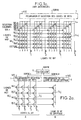
- the zones A and B actually comprise transistors implanted according to a matrix topography, these transistors being respectively connected to a circuit 1 for polarization and for selection of the bit lines and 2 for polarization of the encryption bit line.
- a logical operator denoted C
- the logic operator C is thus connected, to two of its inputs, to output 1 of the bias circuit and selection of bit lines 1, respectively to output 2 of the bias circuit of the bit line encryption 2.
- the first program memory area A is constituted by a network of MOS type transistors, these transistors, being denoted T ij , arranged in the matrix form of row j and column i.
- a line comprises at least one word line, WL j
- a column comprises at least one bit line, BL i .
- the second encryption memory area B includes an encryption bit line. It will of course be understood that, in FIG. 2a, the memory area A represented relates to one bit, the second encryption memory area B then comprising the additional encryption bit line, as will be described in more detail in the description.
- the encryption bit line is formed by transistors, denoted Tc j , which are connected to the encryption bit line, and are of the same type and number identical to those connected to the bit of the first program memory area A.
- the second encryption memory area is constituted by the MOS transistors, Tc j , previously described of the same type and in identical number, the drains of which are connected to a bit line of encryption and grids to word lines WL j .
- FIGS. 2b to 2d various embodiments of the circuits 1 and 2 for polarization and selection of the bit lines have been shown.
- the lines of bit are polarized by the aforementioned circuits, and are therefore kept high by resistors R connected to the supply voltage, VCC, for example.
- P type transistors denoted TP1 and TP2 in FIG. 2c
- CLK clock signal
- type P transistors having a high drain-source resistance and denoted TP2 in FIG. 2c, on the opposite logic level of the clock signal CLK.
- the precharge system can be common to several bit lines.
- the preload is selective, which makes it possible to reduce the dynamic consumption of electrical energy, a single bit line being preloaded during a read cycle, as represented in FIG. 2d, the selection of the bit lines then being sequential.
- connection between the common precharge circuit and the bit lines is then carried out by the selection transistors, denoted TS in FIG. 2d.
- circuit 2 for polarization of the encryption bit line can be produced in a similar manner to the embodiment shown in FIGS. 2b to 2d relative to the circuit 1 for polarization and selection of the bit lines.
- FIG 3 there is shown a first alternative embodiment of the semiconductor program memory read-protected, in accordance with the object of the present invention, as shown in Figure 2a.
- the second memory, or zone encryption memory B is constituted by serial transistors, denoted Tc j , of the same type and in number identical to the number of transistors constituting the columns of transistors associated with each bit line, the second encryption memory being connected to a line of encryption bit, analogously to the embodiment of Figure 2a.
- the memory areas A and B also relate to the memory areas of a bit of given rank, access to a determined column of rank s being thus controlled sequentially by the lines column selection, SEL s , which makes it possible to multiply the number of bits of the same rank thus stored, and ultimately the number of words stored, as will be described later in the description, while reducing the consumption of electrical power supply.
- the circuits for biasing and for selecting bit lines 1 and the encryption bit line 2 are identical to those shown in FIG. 2a or 3.
- the second memory area B can be located either to the right or to the left of the first program memory area A.
- the protected program memory circuit comprises, for each bit, the memory areas A and B previously described in the description.
- the polarization and bit line selection circuits, respectively encryption bit lines 1, 2, have not been shown, so as not to overload the drawing. It is thus understood that for matrix networks constituting the first, A, and second, B, memory areas, matrix networks comprising, as shown in FIG. 5, m rows and n columns, and for k pairs of memory areas A, B , thus implemented, a memory of capacity mxn words of k bits is obtained.
- the encryption bit line or lines and the transistors constituting at least one corresponding column of the encryption bit line of the second encryption memory area B are thus integrated into the network of bit line transistors of the first memory area A, each transistor of one or more columns of the encryption bit line having its gate connected to the gates of the transistors of the first data memory area belonging to the same line, by means of the same word line.
- the fact of constituting the second memory area B in an identical manner from the point of view of the semiconductor architecture to the bit lines or at least to the columns associated with the corresponding bit line of the first memory area A of course allows to make the encryption memory and the memory of program, that is to say zones B and A, indistinguishable from one another by optical observation means.
- the logical operator C can be constituted by an operator of the exclusive OR type.
- the pointing algorithm in the encryption memory can be determined by combinations of address bits of the corresponding program memory.
- unauthorized access and pirating of the program code stored in the memory area A requires knowing both the content of the encryption table and the architecture of the matrix constituting the first memory area A.
- the logical operator comprises k elementary exclusive OR operators for delivering the encrypted data.
- FIG. 6 represents a particular application of an embodiment of a memory in accordance with the object of the present invention, more particularly adapted to the implementation of a microcontroller or a microcomputer.
- a switch 3 is inserted between the circuit 2 for biasing the encryption bit line and the encryption bit line proper.
- This switch 3 can be produced by an N-type transistor capable of switching between a program verification and execution state.
- the switch mechanism previously described makes it possible to isolate each line of encryption bit when the reading of the memory is registered in a program execution cycle. Indeed, only the reading of the code from the outside must be locked, so as to guarantee the protection of the software stored in the program memory against piracy.
- a particularly advantageous read-only memory protected semiconductor program memory has thus been described, insofar as pirating of the program memories can be prevented. This is achieved by the fact that the program memory and the encryption memory are personalized simultaneously, which ensures the uniqueness of the protection and guarantees the confidentiality of the data stored in the program memory area.
Landscapes
- Storage Device Security (AREA)
Applications Claiming Priority (2)
| Application Number | Priority Date | Filing Date | Title |
|---|---|---|---|
| FR9211031A FR2695752B1 (fr) | 1992-09-16 | 1992-09-16 | Mémoire de programme à semi-conducteur protégée en lecture. |
| FR9211031 | 1992-09-16 |
Publications (2)
| Publication Number | Publication Date |
|---|---|
| EP0588700A1 true EP0588700A1 (de) | 1994-03-23 |
| EP0588700B1 EP0588700B1 (de) | 2000-12-27 |
Family
ID=9433562
Family Applications (1)
| Application Number | Title | Priority Date | Filing Date |
|---|---|---|---|
| EP93402217A Expired - Lifetime EP0588700B1 (de) | 1992-09-16 | 1993-09-13 | Lesegeschützter Programmspeicher |
Country Status (4)
| Country | Link |
|---|---|
| US (1) | US5377137A (de) |
| EP (1) | EP0588700B1 (de) |
| DE (1) | DE69329786T2 (de) |
| FR (1) | FR2695752B1 (de) |
Citations (6)
| Publication number | Priority date | Publication date | Assignee | Title |
|---|---|---|---|---|
| EP0040045A1 (de) * | 1980-05-08 | 1981-11-18 | Fujitsu Limited | Festwertspeicheranlage |
| US4318014A (en) * | 1979-07-27 | 1982-03-02 | Motorola, Inc. | Selective precharge circuit for read-only-memory |
| JPS59188897A (ja) * | 1983-04-11 | 1984-10-26 | Hitachi Ltd | デ−タ処理装置におけるデ−タの秘密保護装置 |
| EP0131151A2 (de) * | 1983-06-30 | 1985-01-16 | International Business Machines Corporation | Schaltkreis für einen Hochgeschwindigkeitsleseverstärker mit Blockiermöglichkeit |
| EP0348895A2 (de) * | 1988-06-27 | 1990-01-03 | Nec Corporation | Halbleiterspeichervorrichtung, die mit einer Niederrausch-Spannungsversorgung ausgestattet ist |
| US5131091A (en) * | 1988-05-25 | 1992-07-14 | Mitsubishi Denki Kabushiki Kaisha | Memory card including copy protection |
Family Cites Families (2)
| Publication number | Priority date | Publication date | Assignee | Title |
|---|---|---|---|---|
| US4771462A (en) * | 1987-02-18 | 1988-09-13 | Hannan Forrest A | Communication port encryption/decryption method and apparatus |
| US4987595A (en) * | 1989-09-11 | 1991-01-22 | Motorola, Inc. | Secure cryptographic processor arrangement |
-
1992
- 1992-09-16 FR FR9211031A patent/FR2695752B1/fr not_active Expired - Lifetime
-
1993
- 1993-09-08 US US08/117,761 patent/US5377137A/en not_active Expired - Lifetime
- 1993-09-13 EP EP93402217A patent/EP0588700B1/de not_active Expired - Lifetime
- 1993-09-13 DE DE69329786T patent/DE69329786T2/de not_active Expired - Lifetime
Patent Citations (6)
| Publication number | Priority date | Publication date | Assignee | Title |
|---|---|---|---|---|
| US4318014A (en) * | 1979-07-27 | 1982-03-02 | Motorola, Inc. | Selective precharge circuit for read-only-memory |
| EP0040045A1 (de) * | 1980-05-08 | 1981-11-18 | Fujitsu Limited | Festwertspeicheranlage |
| JPS59188897A (ja) * | 1983-04-11 | 1984-10-26 | Hitachi Ltd | デ−タ処理装置におけるデ−タの秘密保護装置 |
| EP0131151A2 (de) * | 1983-06-30 | 1985-01-16 | International Business Machines Corporation | Schaltkreis für einen Hochgeschwindigkeitsleseverstärker mit Blockiermöglichkeit |
| US5131091A (en) * | 1988-05-25 | 1992-07-14 | Mitsubishi Denki Kabushiki Kaisha | Memory card including copy protection |
| EP0348895A2 (de) * | 1988-06-27 | 1990-01-03 | Nec Corporation | Halbleiterspeichervorrichtung, die mit einer Niederrausch-Spannungsversorgung ausgestattet ist |
Non-Patent Citations (2)
| Title |
|---|
| JACOBSON: "WORD-LINE FAILURE DETECTION CIRCUIT", IBM TECHNICAL DISCLOSURE BULLETIN., vol. 19, no. 11, April 1977 (1977-04-01), NEW YORK US, pages 4197 - 4198 * |
| PATENT ABSTRACTS OF JAPAN vol. 9, no. 50 (P - 339) 5 March 1985 (1985-03-05) * |
Also Published As
| Publication number | Publication date |
|---|---|
| FR2695752B1 (fr) | 1994-11-10 |
| US5377137A (en) | 1994-12-27 |
| FR2695752A1 (fr) | 1994-03-18 |
| EP0588700B1 (de) | 2000-12-27 |
| DE69329786D1 (de) | 2001-02-01 |
| DE69329786T2 (de) | 2001-08-09 |
Similar Documents
| Publication | Publication Date | Title |
|---|---|---|
| EP1434237B1 (de) | Nichtflüchtige SRAM Speicherzelle | |
| EP0666573B1 (de) | Source programmierter nichtflüchtiger Flip-Flop für Speicherredundanzschaltung | |
| FR2660457A1 (fr) | Circuit de protection contre l'effacement et la programmation d'une memoire remanente. | |
| FR2606199A1 (fr) | Circuit integre du type circuit logique comportant une memoire non volatile programmable electriquement | |
| EP0674264B1 (de) | Schaltung zum Wählen von Redundanzspeicherbauelementen und diese enthaltende FLASH EEPROM | |
| FR2655176A1 (fr) | Dispositif de memoire a semiconducteurs programmable et effacable par voie electrique. | |
| FR2464535A1 (fr) | Systeme de memoire statique remanente a acces direct | |
| EP2108163A1 (de) | Schutz von in einer elektronischen schaltung enthaltenen informationen | |
| EP0669576A1 (de) | Speicherredundanzschaltung | |
| EP0544568B1 (de) | Leseschaltkreis für redundante Schmelzsicherung für integrierten Speicher | |
| FR2529702A1 (fr) | Memoire morte a semi-conducteurs | |
| EP0279712B1 (de) | Speicher-Leseschaltung | |
| FR2494887A1 (fr) | Memoire morte programmable | |
| EP0838826B1 (de) | Elektrisch modifizierbarer nichtflüchtiger Mehrpegelspeicher mit internen Auffrischungsmitteln | |
| EP0051525B1 (de) | Logische Anordnung mit vereinfachter elektrischer Programmierung | |
| EP0252794B1 (de) | Anordnung zur Erkennung des Betriebs der Abfühleinrichtung einer EPROM- oder EEPROM-Speicherzelle | |
| EP0875903B1 (de) | Steuerverfahren für eine Speicherzelle mit nur einmal programmierbarem nicht flüchtigen CMOS-Speicher | |
| EP0665559B1 (de) | Nichtflüchtiger programmierbarer Flip-Flop mit Verminderung von parasitären Effekten beim Lesen für Speicherredundanzschaltung | |
| FR2871282A1 (fr) | Dispositif memoire programmable une seule fois | |
| EP0588700B1 (de) | Lesegeschützter Programmspeicher | |
| US20020005563A1 (en) | Fuse structure and application thereof for a CMOS sensor | |
| FR2605447A1 (fr) | Memoire non volatile programmable electriquement | |
| EP0845785A1 (de) | Elektronischer nichtflüchtiger Speicher und Verfahren zur seiner Verwaltung | |
| FR2787911A1 (fr) | Structure differentielle de cellules memoire a programmation unique en technologie cmos | |
| FR2759195A1 (fr) | Circuit de detection de changement d'adresse |
Legal Events
| Date | Code | Title | Description |
|---|---|---|---|
| PUAI | Public reference made under article 153(3) epc to a published international application that has entered the european phase |
Free format text: ORIGINAL CODE: 0009012 |
|
| AK | Designated contracting states |
Kind code of ref document: A1 Designated state(s): DE GB IT NL |
|
| 17P | Request for examination filed |
Effective date: 19940302 |
|
| 17Q | First examination report despatched |
Effective date: 19961216 |
|
| APAB | Appeal dossier modified |
Free format text: ORIGINAL CODE: EPIDOS NOAPE |
|
| APAB | Appeal dossier modified |
Free format text: ORIGINAL CODE: EPIDOS NOAPE |
|
| APAD | Appeal reference recorded |
Free format text: ORIGINAL CODE: EPIDOS REFNE |
|
| APAD | Appeal reference recorded |
Free format text: ORIGINAL CODE: EPIDOS REFNE |
|
| RAP1 | Party data changed (applicant data changed or rights of an application transferred) |
Owner name: MHS |
|
| APAB | Appeal dossier modified |
Free format text: ORIGINAL CODE: EPIDOS NOAPE |
|
| GRAG | Despatch of communication of intention to grant |
Free format text: ORIGINAL CODE: EPIDOS AGRA |
|
| GRAG | Despatch of communication of intention to grant |
Free format text: ORIGINAL CODE: EPIDOS AGRA |
|
| GRAH | Despatch of communication of intention to grant a patent |
Free format text: ORIGINAL CODE: EPIDOS IGRA |
|
| GRAH | Despatch of communication of intention to grant a patent |
Free format text: ORIGINAL CODE: EPIDOS IGRA |
|
| GRAA | (expected) grant |
Free format text: ORIGINAL CODE: 0009210 |
|
| AK | Designated contracting states |
Kind code of ref document: B1 Designated state(s): DE GB IT NL |
|
| REF | Corresponds to: |
Ref document number: 69329786 Country of ref document: DE Date of ref document: 20010201 |
|
| ITF | It: translation for a ep patent filed | ||
| RAP2 | Party data changed (patent owner data changed or rights of a patent transferred) |
Owner name: ATMEL NANTES SA |
|
| GBT | Gb: translation of ep patent filed (gb section 77(6)(a)/1977) |
Effective date: 20010226 |
|
| NLT2 | Nl: modifications (of names), taken from the european patent patent bulletin |
Owner name: ATMEL NANTES SA |
|
| PLBE | No opposition filed within time limit |
Free format text: ORIGINAL CODE: 0009261 |
|
| STAA | Information on the status of an ep patent application or granted ep patent |
Free format text: STATUS: NO OPPOSITION FILED WITHIN TIME LIMIT |
|
| 26N | No opposition filed | ||
| REG | Reference to a national code |
Ref country code: GB Ref legal event code: IF02 |
|
| APAH | Appeal reference modified |
Free format text: ORIGINAL CODE: EPIDOSCREFNO |
|
| PGFP | Annual fee paid to national office [announced via postgrant information from national office to epo] |
Ref country code: NL Payment date: 20090818 Year of fee payment: 17 Ref country code: GB Payment date: 20090904 Year of fee payment: 17 |
|
| PGFP | Annual fee paid to national office [announced via postgrant information from national office to epo] |
Ref country code: IT Payment date: 20090923 Year of fee payment: 17 |
|
| REG | Reference to a national code |
Ref country code: GB Ref legal event code: 732E Free format text: REGISTERED BETWEEN 20100701 AND 20100707 |
|
| REG | Reference to a national code |
Ref country code: NL Ref legal event code: V1 Effective date: 20110401 |
|
| GBPC | Gb: european patent ceased through non-payment of renewal fee |
Effective date: 20100913 |
|
| PG25 | Lapsed in a contracting state [announced via postgrant information from national office to epo] |
Ref country code: IT Free format text: LAPSE BECAUSE OF NON-PAYMENT OF DUE FEES Effective date: 20100913 |
|
| PG25 | Lapsed in a contracting state [announced via postgrant information from national office to epo] |
Ref country code: GB Free format text: LAPSE BECAUSE OF NON-PAYMENT OF DUE FEES Effective date: 20100913 Ref country code: NL Free format text: LAPSE BECAUSE OF NON-PAYMENT OF DUE FEES Effective date: 20110401 |
|
| PGFP | Annual fee paid to national office [announced via postgrant information from national office to epo] |
Ref country code: DE Payment date: 20120927 Year of fee payment: 20 |
|
| REG | Reference to a national code |
Ref country code: DE Ref legal event code: R071 Ref document number: 69329786 Country of ref document: DE |
|
| REG | Reference to a national code |
Ref country code: DE Ref legal event code: R082 Ref document number: 69329786 Country of ref document: DE Representative=s name: GRUENECKER, KINKELDEY, STOCKMAIR & SCHWANHAEUS, DE Effective date: 20130829 Ref country code: DE Ref legal event code: R081 Ref document number: 69329786 Country of ref document: DE Owner name: ATMEL CORPORATION, US Free format text: FORMER OWNER: ATMEL SWITZERLAND S.A.R.L., FRIBOURG, CH Effective date: 20130829 |
|
| PG25 | Lapsed in a contracting state [announced via postgrant information from national office to epo] |
Ref country code: DE Free format text: LAPSE BECAUSE OF EXPIRATION OF PROTECTION Effective date: 20130914 |