EP0589228A1 - Amplificateur de puissance HF - Google Patents
Amplificateur de puissance HF Download PDFInfo
- Publication number
- EP0589228A1 EP0589228A1 EP93113556A EP93113556A EP0589228A1 EP 0589228 A1 EP0589228 A1 EP 0589228A1 EP 93113556 A EP93113556 A EP 93113556A EP 93113556 A EP93113556 A EP 93113556A EP 0589228 A1 EP0589228 A1 EP 0589228A1
- Authority
- EP
- European Patent Office
- Prior art keywords
- output
- power
- arrangement
- variable
- arrangement according
- Prior art date
- Legal status (The legal status is an assumption and is not a legal conclusion. Google has not performed a legal analysis and makes no representation as to the accuracy of the status listed.)
- Withdrawn
Links
Images
Classifications
-
- H—ELECTRICITY
- H03—ELECTRONIC CIRCUITRY
- H03G—CONTROL OF AMPLIFICATION
- H03G3/00—Gain control in amplifiers or frequency changers
- H03G3/20—Automatic control
- H03G3/30—Automatic control in amplifiers having semiconductor devices
- H03G3/3036—Automatic control in amplifiers having semiconductor devices in high-frequency amplifiers or in frequency-changers
- H03G3/3042—Automatic control in amplifiers having semiconductor devices in high-frequency amplifiers or in frequency-changers in modulators, frequency-changers, transmitters or power amplifiers
Definitions
- the invention is based on a high-frequency power amplifier arrangement according to the preamble of the main claim.
- High-frequency power amplifier arrangements of this type are known, for example, as transmitter output stages of television transmitters.
- Such amplifier arrangements have the property that if one or more amplifiers fail, the overall amplifier continues to work with reduced output power, this behavior in the event of interference is very desirable, for example, for television stations as a so-called active reserve.
- the usual control circuits cannot be used, because if the output power of one or more amplifiers decreases, the usual regulation increases the input power of all amplifiers together until the old output power again is reached. The result is an overload of the intact amplifiers and thus a loss of linearity of the overall arrangement or even the possible destruction of the amplifiers.
- a power amplifier arrangement has good interference behavior; in the event of failure of one or more amplifiers, the maximum possible output power is always delivered and nevertheless an overload of the remaining amplifiers is avoided.
- the control arrangement according to the invention can be implemented in a very simple manner with an arbitrarily large control range; all amplifiers are always integrated in the control. This also ensures a high level of operational reliability.
- the regulation according to the invention is suitable both for regulating to constant output power and for regulating to constant amplification of the overall arrangement.
- such a power amplifier arrangement can also be implemented in a very simple manner are protected against the exceeding of any disturbance variables, for this it is only necessary to additionally derive a control variable proportional to this disturbance variable and to include this in the control with the other control variables obtained from the individual amplifiers.
- the overall amplifier arrangement can thus be protected in a particularly simple manner, for example, against faulty terminations at the output (excessive reflection at the amplifier output) or against impermissibly high effective value of the output signal.
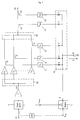
- the figure shows the basic circuit diagram of a high-frequency power amplifier arrangement, as used, for example, for generating a high output power in a television transmitter.
- Couplers B1 and B2 for example decoupling bridges such as Wilkinson couplers, connect a plurality of individual high-frequency power amplifiers V1 to V n , for example conventional transistor amplifiers, in parallel. These individual amplifiers V1 to Vn have the same structure and their amplification properties are practically identical.
- the input power P1 is fed via an actuator S, for example an electronic attenuator and possibly a driver amplifier T to the input of the coupler B1, the output power P2 at the output of the coupler B2 is the sum of all powers of the individual amplifiers V1 to V n .
- each amplifier V1 to V n there is a converter consisting of a directional coupler K with a downstream one Rectifier G switched on, the outputs of these rectifiers G are combined via a decoupling network N, formed here, for example, from the diodes D, at the input E of a controller L.
- the rectifiers G are designed, for example, as peak value rectifiers, but they can also be designed as an RMS rectifier. These converters generate for each individual amplifier V1 to V n at the output of each rectifier an analog voltage U1 to Un which is dependent on the output power of this amplifier, for example the peak voltage U1 to Un corresponding to the peak power at the output of each amplifier. Via the decoupling network N, these DC voltages are fed to the input resistor R of the controller, and a regulating voltage U thus arises at this resistor R, which corresponds to the greatest voltage value of the voltages U1 to Un, this regulating variable U thus corresponds to the output power of the amplifier V1 to Vn with the highest output power.
- This controlled variable U is compared in the controller L, for example with a reference voltage Usoll, and a manipulated variable Ustell is generated at the output of the controller L with which the actuator S is adjusted.
- the reference voltage Usoll is determined, for example, by calculation from the details of the amplifiers V1 to Vn used in each case and corresponds to the nominal target output power value of each individual amplifier.
- the control voltage U practically does not change, since the voltages U1 to Un are decoupled from one another via the diodes D and in each case only the largest voltage am Resistance R drops.
- the controller therefore does not notice a possible failure of one or more amplifiers but regulates the output power of the remaining amplifier with the greatest output power, the input power P1 'practically does not change due to the fault.
- Each amplifier continues to receive its associated input power via the decoupler B1, although the output power P2 drops accordingly if one or more amplifiers fails.
- the remaining output residual power P2 is therefore always the maximum possible residual power of the overall arrangement.
- control circuit to control the overall gain of the arrangement.
- the input power P1 at the input of the overall amplifier is converted into a corresponding DC voltage, for example again the peak value of this input power, via a converter W1 consisting of a directional coupler and a rectifier , implemented and supplied to controller L as a setpoint, as shown by the active connection shown in broken lines. It is then automatically regulated to constant gain.
- the overall amplifier arrangement can also be easily counteracted Any other disturbance variables of the amplifier are protected, for example against a faulty termination at the output of the output decoupler B1. It is only necessary to assign a further directional coupler K1 to the output and to arrange a peak value rectifier G1 at the return output of this directional coupler K1, which therefore supplies a peak voltage value U REFL corresponding to the reflected power of the overall amplifier arrangement , which is fed to a further diode D of the decoupling network.
- a directional coupler K2 is again arranged at the output of the decoupler B2, an RMS rectifier G2 is connected to the forward output of this directional coupler K2, which therefore supplies an RMS voltage U EFF corresponding to the RMS value of the output signal of the overall amplifier arrangement , which in turn supplies the diode via a diode Decoupling network N is supplied.
- this effective value U EFF thus obtained is greater than one of the peak voltage values U1 to Un obtained in this case via peak value rectifier G, then this largest controlled variable U EFF again takes over the control and the input power of the overall amplifier arrangement is reduced via the actuator S, so that the amplifier counteracts inadmissibly high effective value is protected.
- the voltages U REFL and U EFF could also be generated individually for each amplifier in a similar way to the voltages U1 to Un and passed to the resistor R via the decoupling network N.
- the amplifier could also be protected in the same way against other disturbance variables, for example the temperature, by using a temperature converter to obtain a control voltage corresponding to the temperature and to supply it to the decoupling network N when the amplifier is heated to an excessively high temperature, which in turn takes on the highest temperature Temperature control variable controlling the output power and the amplifier is thus protected against overheating.
Landscapes
- Amplifiers (AREA)
Applications Claiming Priority (2)
| Application Number | Priority Date | Filing Date | Title |
|---|---|---|---|
| DE4231925 | 1992-09-24 | ||
| DE19924231925 DE4231925C1 (de) | 1992-09-24 | 1992-09-24 | Hochfrequenz-Leistungsverstärker-Anordnung |
Publications (1)
| Publication Number | Publication Date |
|---|---|
| EP0589228A1 true EP0589228A1 (fr) | 1994-03-30 |
Family
ID=6468680
Family Applications (1)
| Application Number | Title | Priority Date | Filing Date |
|---|---|---|---|
| EP93113556A Withdrawn EP0589228A1 (fr) | 1992-09-24 | 1993-08-25 | Amplificateur de puissance HF |
Country Status (2)
| Country | Link |
|---|---|
| EP (1) | EP0589228A1 (fr) |
| DE (1) | DE4231925C1 (fr) |
Cited By (2)
| Publication number | Priority date | Publication date | Assignee | Title |
|---|---|---|---|---|
| EP0982852A3 (fr) * | 1998-08-19 | 2004-03-17 | Harris Corporation | Amplificateur de puissance avec moniteur et circuit de protection |
| EP1411631A3 (fr) * | 2002-10-16 | 2005-02-02 | Lg Electronics Inc. | Système d'amplification de puissance et méthode correspondante |
Families Citing this family (2)
| Publication number | Priority date | Publication date | Assignee | Title |
|---|---|---|---|---|
| DE4434903A1 (de) * | 1994-09-29 | 1996-04-11 | Hirschmann Richard Gmbh Co | Schaltungsanordnung für die Satellitenkommunikation |
| DE19535868A1 (de) * | 1995-09-27 | 1997-04-03 | Thomson Brandt Gmbh | Schaltung zur Stromversorgung mehrerer Leistungsverstärker |
Citations (5)
| Publication number | Priority date | Publication date | Assignee | Title |
|---|---|---|---|---|
| FR2220111A1 (fr) * | 1973-03-01 | 1974-09-27 | Licentia Gmbh | |
| US3900823A (en) * | 1973-03-28 | 1975-08-19 | Nathan O Sokal | Amplifying and processing apparatus for modulated carrier signals |
| FR2310656A1 (fr) * | 1975-05-03 | 1976-12-03 | Licentia Gmbh | Montage permettant la reunion de composantes de puissance haute frequence |
| SU1587617A1 (ru) * | 1988-04-18 | 1990-08-23 | Московский институт радиотехники, электроники и автоматики | Многоканальный СВЧ-усилитель |
| US5136300A (en) * | 1991-06-13 | 1992-08-04 | Westinghouse Electric Corp. | Modular solid state radar transmitter |
Family Cites Families (1)
| Publication number | Priority date | Publication date | Assignee | Title |
|---|---|---|---|---|
| DE3335170C2 (de) * | 1983-09-28 | 1986-08-21 | Siemens AG, 1000 Berlin und 8000 München | Leistungsverstärker für kurze elektromagnetische Wellen |
-
1992
- 1992-09-24 DE DE19924231925 patent/DE4231925C1/de not_active Expired - Lifetime
-
1993
- 1993-08-25 EP EP93113556A patent/EP0589228A1/fr not_active Withdrawn
Patent Citations (5)
| Publication number | Priority date | Publication date | Assignee | Title |
|---|---|---|---|---|
| FR2220111A1 (fr) * | 1973-03-01 | 1974-09-27 | Licentia Gmbh | |
| US3900823A (en) * | 1973-03-28 | 1975-08-19 | Nathan O Sokal | Amplifying and processing apparatus for modulated carrier signals |
| FR2310656A1 (fr) * | 1975-05-03 | 1976-12-03 | Licentia Gmbh | Montage permettant la reunion de composantes de puissance haute frequence |
| SU1587617A1 (ru) * | 1988-04-18 | 1990-08-23 | Московский институт радиотехники, электроники и автоматики | Многоканальный СВЧ-усилитель |
| US5136300A (en) * | 1991-06-13 | 1992-08-04 | Westinghouse Electric Corp. | Modular solid state radar transmitter |
Non-Patent Citations (1)
| Title |
|---|
| DATABASE WPI Week 9128, Derwent World Patents Index; AN 91-206339 * |
Cited By (3)
| Publication number | Priority date | Publication date | Assignee | Title |
|---|---|---|---|---|
| EP0982852A3 (fr) * | 1998-08-19 | 2004-03-17 | Harris Corporation | Amplificateur de puissance avec moniteur et circuit de protection |
| EP1411631A3 (fr) * | 2002-10-16 | 2005-02-02 | Lg Electronics Inc. | Système d'amplification de puissance et méthode correspondante |
| US7177659B2 (en) | 2002-10-16 | 2007-02-13 | Lg Electronics Inc. | Power amplification system and method |
Also Published As
| Publication number | Publication date |
|---|---|
| DE4231925C1 (de) | 1994-01-27 |
Similar Documents
| Publication | Publication Date | Title |
|---|---|---|
| DE10214190B4 (de) | Stromversorgung mit mehreren parallel geschalteten Schaltnetzteilen | |
| DE69226340T2 (de) | Leistungssystem zum Parallelbetrieb von Wechselstrom-Gleichstrom-Umwandlern | |
| DE3015610A1 (de) | Schaltung zur regelung eines gleichstroms | |
| DE3320885A1 (de) | Parallelbetriebssysteme fuer stabilisierte leistungsquellen | |
| DE2519845C3 (de) | Schaltungsanordnung zur Zusammenführung von Hochfrequenzleistungsanteilen | |
| DE3789977T2 (de) | Niederfrequenz-Leistungsverstärker, insbesondere in integrierter Ausführung. | |
| DE2438883A1 (de) | Rueckgekoppelter verstaerker | |
| DE19506405C1 (de) | Stromversorgungseinrichtung | |
| DE4231925C1 (de) | Hochfrequenz-Leistungsverstärker-Anordnung | |
| EP0692757B1 (fr) | Circuit pour fournir des tensions d'alimentations | |
| DE102005058039A1 (de) | Schaltungsanordnung und Verfahren zur Verstärkung eines elektrischen Eingangssignals | |
| DE2624337C2 (de) | Doppelgegentaktmodulator mit einem Gegentaktverstärker | |
| DE4037722C1 (en) | Current supply circuitry with no mains transformer - has controlled transistor acting as limiting stage across output of rectifier stage | |
| DE3803583A1 (de) | Schaltverstaerker zur digitalen leistungsverstaerkung | |
| DE4308287C2 (de) | Elektrischer Leistungsverstärker und Verfahren zu dessen Betrieb | |
| EP0985260B1 (fr) | Circuit de commutation pour unite d'alimentation en courant fournissant des tensions de sortie couplees et rajustees de maniere lineaire | |
| DE69702348T2 (de) | Leistungsverstärker | |
| DE2007694C3 (de) | Spannungsregelgerät mit schaltendem Stellglied | |
| DE2838062C2 (de) | Anordnung mit parallelgeschalteten Gleichstrom-Umrichtern | |
| DE3246144C2 (de) | Schaltungsanordnung zur Stromkonstanthaltung | |
| DE19547155C1 (de) | Elektrische Schaltungsanordnung zur Umformung einer Eingangsspannung | |
| EP0819273B1 (fr) | Repartition de courants d'alimentation | |
| EP1148626A2 (fr) | Alimentation de puissance à découpage avec tension de sortie réglée | |
| EP0885480B1 (fr) | Circuit pour alimentation a decoupage presentant plusieurs tensions de sortie independantes de la charge | |
| DE3806968A1 (de) | Verfahren und schaltungsanordnung zur erzeugung einer geregelten ausgleichsspannung aus einer hoeheren eingangsgleichspannung |
Legal Events
| Date | Code | Title | Description |
|---|---|---|---|
| PUAI | Public reference made under article 153(3) epc to a published international application that has entered the european phase |
Free format text: ORIGINAL CODE: 0009012 |
|
| AK | Designated contracting states |
Kind code of ref document: A1 Designated state(s): DE ES FR GB IT |
|
| 17P | Request for examination filed |
Effective date: 19940223 |
|
| 18W | Application withdrawn |
Withdrawal date: 19941217 |