EP0589251A2 - Verfahren und Gerät zur Erzeugung von mehrphasigen Entflimmerungswellen auf der Basis von Impulsbreitenverhältnissen - Google Patents
Verfahren und Gerät zur Erzeugung von mehrphasigen Entflimmerungswellen auf der Basis von Impulsbreitenverhältnissen Download PDFInfo
- Publication number
- EP0589251A2 EP0589251A2 EP93113990A EP93113990A EP0589251A2 EP 0589251 A2 EP0589251 A2 EP 0589251A2 EP 93113990 A EP93113990 A EP 93113990A EP 93113990 A EP93113990 A EP 93113990A EP 0589251 A2 EP0589251 A2 EP 0589251A2
- Authority
- EP
- European Patent Office
- Prior art keywords
- phase
- waveform
- multiphasic
- capacitor
- voltage
- Prior art date
- Legal status (The legal status is an assumption and is not a legal conclusion. Google has not performed a legal analysis and makes no representation as to the accuracy of the status listed.)
- Granted
Links
Images


Classifications
-
- A—HUMAN NECESSITIES
- A61—MEDICAL OR VETERINARY SCIENCE; HYGIENE
- A61N—ELECTROTHERAPY; MAGNETOTHERAPY; RADIATION THERAPY; ULTRASOUND THERAPY
- A61N1/00—Electrotherapy; Circuits therefor
- A61N1/18—Applying electric currents by contact electrodes
- A61N1/32—Applying electric currents by contact electrodes alternating or intermittent currents
- A61N1/38—Applying electric currents by contact electrodes alternating or intermittent currents for producing shock effects
- A61N1/39—Heart defibrillators
- A61N1/3956—Implantable devices for applying electric shocks to the heart, e.g. for cardioversion
-
- A—HUMAN NECESSITIES
- A61—MEDICAL OR VETERINARY SCIENCE; HYGIENE
- A61N—ELECTROTHERAPY; MAGNETOTHERAPY; RADIATION THERAPY; ULTRASOUND THERAPY
- A61N1/00—Electrotherapy; Circuits therefor
- A61N1/18—Applying electric currents by contact electrodes
- A61N1/32—Applying electric currents by contact electrodes alternating or intermittent currents
- A61N1/38—Applying electric currents by contact electrodes alternating or intermittent currents for producing shock effects
- A61N1/39—Heart defibrillators
- A61N1/3906—Heart defibrillators characterised by the form of the shockwave
Definitions
- the present invention relates to cardioversion/defibrillation systems and more particularly to a method and apparatus for generating multiphasic defibrillation waveforms.
- the present invention is directed to a method and apparatus for generating a multiphasic defibrillation/ cardioversion waveform by specifying only the initial voltage and end voltage of the first phase and the percentage of pulse widths for each subsequent phase relative to the pulse width of the first phase. Therefore, only two voltage measurements need to be made for the first phase, while for the remaining phases, only the time duration (pulse width) is detected.
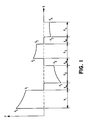
- Figure 1 is a graphical representation of a multiphasic defibrillation waveform which is generated by the method and apparatus according to the present invention.
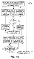
- Figure 2 is a flow chart illustrating the steps of generating a multiphasic defibrillation/cardioversion waveform according to the present invention.
- Figure 3 is a schematic diagram of circuitry for generating a multiphasic defibrillation waveform according to the present invention.
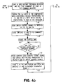
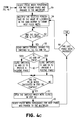
- Figure 4 is a flow chart illustrating the operation of the circuitry shown in Figure 3.
- a multiphasic defibrillation waveform comprising four phases.
- the waveform shown in Figure 1 is generated by specifying the initial voltage V0, the first truncate voltage V1 and the pulse width of each of the phases 2 through 4 as a percentage of the pulse width of phase 1. Consequently, only two voltage measurements must be performed by the waveform generating circuitry and over a small voltage range (V0 to V1). Moreover, the time measurements may be accomplished more reliably and accurately for the higher order phases (phases 2-4) using much simpler hardware.
- phase 1 would be specified in terms of the initial voltage V0 and the truncate voltage V1, and the higher order phases (n ⁇ 2) are specified as a percentage of t1 where t1 is the time duration (also referred to as pulse width) of the first phase.
- the cutoff or truncate voltage of each phase is directly related to a percentage of the pulse width of the initial phase and is independent of the actual time and RC time constant. With the knowledge of the initial and final voltages and the capacitance, the total energy delivered by the multiphase waveform can be calculated.
- step 20 the initial voltage level V0 of the first phase is set, which voltage level also corresponds to the initial voltage level of the capacitor.
- each pulse width percentage P2, P3, ..., P n is set for each phase, each pulse width percentage P2, P3, ..., P n being a ratio of the duration of the respective phase to the time duration t1 of the first phase of the multiphasic waveform.
- each of the pulse width percentages P2, P3, ..., P n can be calculated from the desired cutoff or truncate voltage of each phase, knowing the initial voltage and the termination voltage of the first phase.
- step 22 the termination voltage V1 is set for the first phase of the multiphasic waveform.
- step 23 the capacitor is charged to the initial voltage V0 of the first phase.
- step 24 the capacitor is discharged from its initial voltage V0 to the termination voltage V1 hence providing the first phase of the multiphasic waveform.
- step 25 the time duration of the first phase is determined.
- step 26 the time durations t22 t3, ..., t n for subsequent phases are computed by multiplying each of the pulse width percentages P2, P3, ..., P n by the time duration t1 of the first phase.
- phase 27 subsequent phases of the multiphasic waveform are generated by discharging the capacitor for the time durations computed in step 26. Specifically, the phases are generated with alternating polarity, for example, positive polarity for odd values of n and negative polarity for even values of n.
- FIG. 3 illustrates electrical circuitry for generating a multiphasic defibrillation waveform according to the present invention.
- the circuitry 100 comprises a microprocessor 102; a set of addressable registers 104 connected to the microprocessor 102; a multiplexer (MUX) 106; charge control logic 108; a multiplier 110; a data buffer 112; a digital to analog converter (DAC) 114; a timer 116; pulse control logic 118; a comparator 120; a voltage divider 122; a high voltage supply 124; high voltage translators 126; a 125 to 150 microfarad capacitor 128; four switches S1, S2, S3, and S4; and two defibrillation electrodes D+ and D- located in close proximity to a patient's heart 130.
- MUX multiplexer
- DAC digital to analog converter
- the circuitry 100 is primarily controlled by the microprocessor 102 which itself can be either directly preprogrammed by a physician with values for V0, V1, P2, P3, ..., P n or indirectly preprogrammed using other parameters provided by the physician through means well known in the art.
- the physician for example, could specify percentage tilt, voltages, and/or pulse width percentages, while an external module takes these values and calculates the proper values for V0, V1, P2, P3, ..., P n on behalf of the microprocessor 102.
- This data is then fed to the microprocessor 102, which either causes a defibrillation shock to be delivered immediately or causes one to be delivered automatically in response to a detected cardiac arrhythmia.
- a preferred microprocessor 102 is the model 68HC11 manufactured by Motorola.
- the set of addressable registers 104 is connected to the microprocessor 102 and comprises a voltage threshold register for storing the values V0 and V1; a pulse width percentage register for storing each of the values P2, P3, ..., P n ; a command register for storing a "charge command" bit code or a "fire command” bit code; and a register for storing t1.
- the microprocessor 102 by first storing the values for either V0 or V1, along with P2, P3, ..., P n in the set of addressable registers 104, and then selectively storing either the "fire command" bit code or the "charge command” bit code in the command register, is able to cause either delivery of a desired multiphasic defibrillation shock or the charging of the capacitor 128 to the desired peak voltage V0 of the first phase, respectively.
- the digital to analog converter (DAC) 114 is responsive to the value of V0 or V1 whichever is digitally stored in the voltage threshold register.
- the primary function of the DAC 114 is to take this digital value for V0 or V1, and in accordance therewith, provide an output reference voltage proportional to the desired peak value V0 or termination value V1 of the first phase. This output reference voltage is within the input range of, and is fed into, the positive input of the comparator 120.
- the charge control logic 108 is responsive to the output from the comparator 120 and the bit code contained in the command register, so as to selectively enable the high voltage supply 124. By selectively enabling the high voltage supply 124 in response to detecting a "charge command" bit code in the command register, the charge control logic 108 is able to cause charging of the capacitor 128 to the peak voltage V0 of the first phase.
- the high voltage supply itself is well known to the art.
- the charge control logic 108 is a sequencer which powers up the analog circuit and then charges the capacitor 128 until the comparator 120 switches.
- the voltage divider 122 comprises two series-connected resistors r1 and r2 arranged such that the voltage present across the capacitor 128 is also applied across the series-connected resistors r1 and r2.
- the resistors have resistance values ranging from 9.7M to 10.7M ohms for r1, and 15K to 25K ohms for r2. More specifically though, the value of each resistor r1 and r2 is chosen such that the voltage at the center tap (the voltage across r2 at a ratio of 480 plus or minus 2 percent) is at a level within the input range of the comparator 120. This center tap voltage is then fed into the negative input of the comparator 120, and as a result, the negative input of the comparator 120 receives a voltage proportional to, but smaller than, that which is present across the capacitor 128.
- the timer 116 is connected and responsive to the pulse control logic 118 such that, upon commencement of the first phase, the timer 116 begins counting elapsed time.
- the timer's output is connected to the data buffer 112 and is thereby able to provide the data buffer 112 with a measure of the time elapsed after application of the first phase. This measure of elapsed time is also provided to the pulse control logic 118.
- the data buffer 112 is connected to the pulse control logic 118 via a "store" signal, and is responsive to the "store” signal such that upon the signal being applied, the data buffer 112 stores the current value of the timer's output. Since the "store" signal is applied, as will be discussed hereinafter, upon termination of the first phase, the stored value corresponds to the pulse width t1 of the first phase.
- the multiplexer (MUX) 106 is responsive to a "percentage select" signal from the pulse control logic 118 and, in accordance therewith, selects one of the pulse width percentage values P2, P3, ..., or P n from the corresponding register. The selected pulse width percentage P2, P3, ..., or P n is then supplied to the multiplier 110.
- the multiplier 110 is connected to both the data buffer 102 and the multiplexer 106. As a result, the multiplier 110 receives both the selected pulse width percentage value P2, P3, ..., or P n from the multiplexer 106 and the stored value corresponding to the pulse width t1 °f the first phase. Both of these values are multiplied by the multiplier 110 with the result being provided to the pulse control logic 118.
- the pulse control logic 118 is connected and responsive to the command register, the result from the multiplier 110, the elapsed time measured by the timer 116, and the output from the comparator 120. In addition, the pulse control logic 118 provides the "percentage select" signal to the multiplexer 106, the "store” signal to the data buffer 112, and four low voltage control signals to the high voltage translators 126.
- the pulse control logic 118 is a digital logic sequencer that controls the pulse generator circuitry 106, 110, 112, 116 and 126.
- the high voltage translators 126 are connected and receive the four low voltage control signals from the pulse control logic 118. In response to the low voltage control signals, the high voltage translators 126 produce four switch control signals corresponding to the low voltage control signals, but of higher voltage. In this regard, the translators 126 simply step-up the voltage of the low voltage control signals.
- each of the switch control signals is connected to one of the switches S1, S2, S3, and S4.
- the switches S1, S2, S3, and S4 are arranged and responsive to the switch control signals so as to selectively make or break a series electrical circuit through the heart 130, the capacitor 128, and the defibrillation electrodes D+ and D-.
- the circuitry 100 either provides the heart 130 with a positive polarity voltage (where D- is connected to ground) or a negative polarity voltage (where D+ is connected to ground).
- closing switches s1 and s4 provides the heart 130 with a positive polarity voltage
- closing switches s2 and s3 provides a negative polarity voltage.
- step 30 the microprocessor 102 loads the peak voltage value V0 into the voltage threshold register, and sets the "charge command" bit code into the command register.
- V0 depends on several external factors including electrode configuration, the patient's defibrillation threshold, patient and electrode impedances, etc. Nevertheless, typical values for V0 range from 45 to 715 volts.
- step 32 the DAC 114 detects the value V0 and, in response thereto, creates the output reference voltage proportional to the desired peak voltage value V0 of the first phase, the reference voltage being provided to the positive input of the comparator 120. Meanwhile, the voltage divider 122 divides the voltage present on the capacitor 128 to a level within the input range of the comparator 120, and provides this lower voltage to the negative input of the comparator 120.
- the charge control logic 108 detects the output from the comparator 120, and in response to this output selectively enables the high voltage supply 124. More specifically, when the voltage across the capacitor 128 is less than V0, the input to the negative terminal of the comparator 120 is less than that of the positive terminal. This, in turn, causes a high output on the comparator 120. The charge control logic 108 responds to this high output by enabling the high voltage supply 124 which begins charging the capacitor 128. If, on the other hand, the comparator's output begins low, then this may be an indication that the capacitor 128 is over-charged. Accordingly, the capacitor 128 is discharged through a dump resistor (not shown), which can be of any design generally known in the art. Examples of such dump resistors are shown in U.S. Patents Nos. 4,316,472 and 4,488,555 to Imran and Mirowski, respectively.
- step 36 when the voltage on the capacitor 128 reaches V0 while being charged, the comparator's output goes from high to low, signalling the charge control logic 108 to disable the high voltage supply 124. A signal from the charge control logic 108 is provided to the microprocessor 102 when the capacitor 128 is fully charged.
- step 38 the microprocessor 102 loads the first phase termination voltage value V1 into the voltage threshold register and sets the "fire command" bit code in the command register.
- V1 the first phase termination voltage value
- V1 the voltage threshold register
- the actual value for V1 depends upon several external factors, but nevertheless may range between 18 and 286 volts.
- step 40 the DAC 114 detects the digitally stored value for V1 and, in response thereto, creates a reference voltage proportional to the termination voltage V1 of the first phase, the reference voltage being provided to the positive input of the comparator 120.
- the voltage divider 122 continues to divide the voltage present on the capacitor 128 to a level within the input range of the comparator 120, and provides this lower voltage to the negative input of the comparator 120.
- step 42 upon detecting the "fire command" bit code in the command register, the pulse control logic 118 sends appropriate control signals to the switches S1, S2, S3, and S4 through the high voltage translators 126, which signals are output by the translators 126 as higher voltage switch control signals.
- step 44 the switch control signals cause the switches S1 and S4 to close, thus creating a positive polarity series circuit through the capacitor 128, the heart 130, and the defibrillation electrodes D+ and D-.
- the capacitor 128 begins to discharge through the heart 130 thereby commencing the first phase of the multiphasic defibrillation shock.
- step 46 while the first phase is being applied to the heart 130, the timer 116 counts elapsed time and the pulse control logic 118 detects the output from the comparator 120 awaiting a transition from a low output to a high output.
- the comparator 120 output goes from low to high, thereby signalling the pulse control logic 118 to open the switches S1 and S4 and terminate the first phase.
- step 50 the pulse control logic 118 detects the low to high transition in the comparator's output, and in response thereto, sends the "store" signal to the data buffer 112.
- the pulse control logic 118 further causes a set of switch control signals to be sent from the high voltage translators 126 to open switches S1 and S4.
- step 52 upon receiving the "store signal", the data buffer 112 stores the elapsed time corresponding to the pulse width t1 of the first phase.
- the pulse width t1 may be between 1 and 24 milliseconds long.
- the switches S1 and S4 are opened to prevent further discharge of the capacitor 12 8 and to thereby terminate the first phase.
- step 54 the pulse control logic 118, using the "percentage select" signal, causes the multiplexer (Mm) 106 to select the second pulse width percentage P2 from the corresponding register, which pulse width percentage P2 is provided to the multiplier 110 for multiplication with the first phase pulse width t1.
- step 56 the multiplier 110 receives the value of P2 from the multiplexer 106, as well as the value of t1 from the data buffer 112, and multiplies both values to obtain a result which corresponds to the pulse width t2 of the second phase, this result t2 being provided to the pulse control logic 118.
- step 58 after a delay time t d , the pulse control logic 118 sends appropriate control signals to the switches S1, S2, S3, and S4 through the high voltage translators 126, which signals are output by the translators 126 as higher voltage switch control signals.
- step 60 the switch control signals emitted in step 58 cause switches S2 and S3 (since the value of n is even) to close thus creating a negative polarity series circuit through the capacitor 128, the heart 130, and the defibrillation electrodes D+ and D-.
- the capacitor 128 again begins to discharge through the heart 130, but this time with negative polarity.
- the second phase of the multiphasic defibrillation shock is thereby commenced.
- step 61 at the end of the pulse width t2, the pulse control logic 118 causes the switches S2 and S3 to open, thus terminating the second phase of the multiphasic shock.
- step 62 the next consecutive pulse width percentage P3, P4, ..., or P n is selected using the multiplexer 106, and the steps 56 - 61 are repeated for each value of P3, P4, ..., or P n and each value of t3, ..., t4, or t n or tn until the final percentage Pn has been selected and the last phase has been delivered to the heart 130 with the respective pulse width t n .
- step 60 is repeated for odd values of n, switches S1 and S4 are closed to deliver a positive polarity voltage to the heart 130. For even values of n, switches S2 and S3 are closed to deliver a negative polarity voltage to the heart 130. In this manner, successive phases continue to alternate polarity until the last phase has been delivered.
- the pulse width percentages P2, P3, P4, ..., P n preferably range in value from 25% to 150% such that the pulse widths t2, t3, ..., t n range in value from to 1 to 36 milliseconds.
- the delay time t d ranges from 0.8 to 1.2 milliseconds.
- the external programmer 150 and other similar devices can also be used to program the values of V0, V1, P2, P3, ..., P n into the microprocessor 102 of the present invention. Programming of defibrillator operating parameters using an external programmer device is well known in the art.
- circuitry 100 shown in Figure 3 without departing from the scope and spirit of the present invention.
- many functions performed by the microprocessor 102 may be performed by analog circuitry.
- the charging and discharging of the capacitor 128 may actually be accomplished using two separate circuits, one circuit for charging the capacitor 128 and one circuit for enabling and disabling the discharge of the capacitor 128.
Landscapes
- Health & Medical Sciences (AREA)
- Cardiology (AREA)
- Heart & Thoracic Surgery (AREA)
- Engineering & Computer Science (AREA)
- Biomedical Technology (AREA)
- Nuclear Medicine, Radiotherapy & Molecular Imaging (AREA)
- Radiology & Medical Imaging (AREA)
- Life Sciences & Earth Sciences (AREA)
- Animal Behavior & Ethology (AREA)
- General Health & Medical Sciences (AREA)
- Public Health (AREA)
- Veterinary Medicine (AREA)
- Electrotherapy Devices (AREA)
- Magnetic Treatment Devices (AREA)
Applications Claiming Priority (2)
| Application Number | Priority Date | Filing Date | Title |
|---|---|---|---|
| US95125292A | 1992-09-25 | 1992-09-25 | |
| US951252 | 1992-09-25 |
Publications (3)
| Publication Number | Publication Date |
|---|---|
| EP0589251A2 true EP0589251A2 (de) | 1994-03-30 |
| EP0589251A3 EP0589251A3 (de) | 1994-12-14 |
| EP0589251B1 EP0589251B1 (de) | 2000-11-02 |
Family
ID=25491487
Family Applications (1)
| Application Number | Title | Priority Date | Filing Date |
|---|---|---|---|
| EP93113990A Expired - Lifetime EP0589251B1 (de) | 1992-09-25 | 1993-09-01 | Gerät zur Erzeugung von mehrphasigen Entflimmerungswellen auf der Basis von Impulsbreitenverhältnissen |
Country Status (6)
| Country | Link |
|---|---|
| EP (1) | EP0589251B1 (de) |
| JP (1) | JPH06292734A (de) |
| AT (1) | ATE197251T1 (de) |
| AU (1) | AU4612693A (de) |
| CA (1) | CA2106948C (de) |
| DE (1) | DE69329612T2 (de) |
Cited By (2)
| Publication number | Priority date | Publication date | Assignee | Title |
|---|---|---|---|---|
| EP0641573A3 (de) * | 1993-08-31 | 1997-06-25 | Ventritex Inc | Verfahren und Gerät zur Herzdefibrillation mit verwandten Phasen. |
| WO1997026044A1 (en) * | 1996-01-16 | 1997-07-24 | Medtronic, Inc. | Method and apparatus for induction of fibrillation |
Families Citing this family (4)
| Publication number | Priority date | Publication date | Assignee | Title |
|---|---|---|---|---|
| WO2015127466A2 (en) | 2014-02-24 | 2015-08-27 | Element Science, Inc | External defibrillator |
| EP3340862B1 (de) | 2015-08-26 | 2023-06-07 | Element Science, Inc. | Am körper tragbare defibrillator-vorrichtungen |
| US10946207B2 (en) | 2017-05-27 | 2021-03-16 | West Affum Holdings Corp. | Defibrillation waveforms for a wearable cardiac defibrillator |
| EP4438108B1 (de) | 2018-10-10 | 2026-04-29 | Element Science, Inc. | Verfahren zur verwendung eines tragbaren medizinischen geräts mit einweg- und wiederverwendbaren komponenten |
Family Cites Families (5)
| Publication number | Priority date | Publication date | Assignee | Title |
|---|---|---|---|---|
| US4800883A (en) * | 1986-04-02 | 1989-01-31 | Intermedics, Inc. | Apparatus for generating multiphasic defibrillation pulse waveform |
| US4821723A (en) * | 1987-02-27 | 1989-04-18 | Intermedics Inc. | Biphasic waveforms for defibrillation |
| US4850357A (en) * | 1988-01-12 | 1989-07-25 | Cardiac Pacemakers, Inc. | Biphasic pulse generator for an implantable defibrillator |
| US4998531A (en) * | 1990-03-28 | 1991-03-12 | Cardiac Pacemakers, Inc. | Implantable N-phasic defibrillator output bridge circuit |
| EP0491649B1 (de) * | 1990-12-18 | 1996-09-25 | Ventritex | Gerät zur Herstellung konfigurierbarer, zweiphasiger Entflimmerungswellenformen |
-
1993
- 1993-09-01 DE DE69329612T patent/DE69329612T2/de not_active Expired - Fee Related
- 1993-09-01 EP EP93113990A patent/EP0589251B1/de not_active Expired - Lifetime
- 1993-09-01 AT AT93113990T patent/ATE197251T1/de not_active IP Right Cessation
- 1993-09-06 AU AU46126/93A patent/AU4612693A/en not_active Abandoned
- 1993-09-24 CA CA002106948A patent/CA2106948C/en not_active Expired - Fee Related
- 1993-09-27 JP JP5239798A patent/JPH06292734A/ja active Pending
Cited By (2)
| Publication number | Priority date | Publication date | Assignee | Title |
|---|---|---|---|---|
| EP0641573A3 (de) * | 1993-08-31 | 1997-06-25 | Ventritex Inc | Verfahren und Gerät zur Herzdefibrillation mit verwandten Phasen. |
| WO1997026044A1 (en) * | 1996-01-16 | 1997-07-24 | Medtronic, Inc. | Method and apparatus for induction of fibrillation |
Also Published As
| Publication number | Publication date |
|---|---|
| CA2106948A1 (en) | 1994-03-26 |
| JPH06292734A (ja) | 1994-10-21 |
| DE69329612T2 (de) | 2001-05-03 |
| EP0589251A3 (de) | 1994-12-14 |
| AU4612693A (en) | 1994-03-31 |
| ATE197251T1 (de) | 2000-11-15 |
| CA2106948C (en) | 2001-04-17 |
| EP0589251B1 (de) | 2000-11-02 |
| DE69329612D1 (de) | 2000-12-07 |
Similar Documents
| Publication | Publication Date | Title |
|---|---|---|
| EP0491649B1 (de) | Gerät zur Herstellung konfigurierbarer, zweiphasiger Entflimmerungswellenformen | |
| US5824018A (en) | Fibrillation induction method and system for implantable devices | |
| US5372606A (en) | Method and apparatus for generating adaptive n-phasic defibrillation waveforms | |
| US5531765A (en) | Method and apparatus for producing configurable biphasic defibrillation waveforms | |
| EP0588126B1 (de) | Implantierbares Herz-Defibrillationsgerät | |
| US6241751B1 (en) | Defibrillator with impedance-compensated energy delivery | |
| EP0553863B1 (de) | Dualkapazität-Zweiphasen-Wellenformerzeuger zur Entflimmerung unter Verwendung von selektivem Anschluss von Kondensatoren für jede Phase | |
| US5385575A (en) | Implantable cardioverter defibrillator having variable output capacitance | |
| US5999852A (en) | Defibrillator method and apparatus | |
| US6128531A (en) | Delivery of ICD shock capacitor energy via a controlled current source | |
| US5391186A (en) | Method and apparatus for utilizing short tau capacitors in an implantable cardioverter defibrillator | |
| US5458619A (en) | Apparatus and method for treating a tachyarrhythmia | |
| US5137021A (en) | Lead current measurement circuit | |
| EP0315368B1 (de) | Auf Stromfluss gegründeter Defibrillator | |
| US5395395A (en) | Method and apparatus for increasing the energy output from a bank of capacitors | |
| JPH0647100A (ja) | 生体組織に電気パルスを印加する装置 | |
| US6104954A (en) | High frequency lead testing apparatus in an implantable defibrillator | |
| WO2003047685A2 (en) | Control of arbitrary waveforms for constant delivered energy | |
| US5360435A (en) | Multiple pulse cardioversion or defibrillation | |
| JPS6150465B2 (de) | ||
| US20030125771A1 (en) | Multiphasic defibrillator utilizing controlled energy pulses | |
| EP0589251B1 (de) | Gerät zur Erzeugung von mehrphasigen Entflimmerungswellen auf der Basis von Impulsbreitenverhältnissen | |
| US5350405A (en) | Method and apparatus for capacitor tolerance compensation in a cardiac stimulating device | |
| US5653740A (en) | Method and apparatus for induction of fibrillation | |
| US6487448B2 (en) | Method and apparatus for converting a monophasic defibrillator to a biphasic defibrillator |
Legal Events
| Date | Code | Title | Description |
|---|---|---|---|
| PUAI | Public reference made under article 153(3) epc to a published international application that has entered the european phase |
Free format text: ORIGINAL CODE: 0009012 |
|
| AK | Designated contracting states |
Kind code of ref document: A2 Designated state(s): AT BE CH DE DK ES FR GB GR IE IT LI LU MC NL PT SE |
|
| PUAL | Search report despatched |
Free format text: ORIGINAL CODE: 0009013 |
|
| AK | Designated contracting states |
Kind code of ref document: A3 Designated state(s): AT BE CH DE DK ES FR GB GR IE IT LI LU MC NL PT SE |
|
| 17P | Request for examination filed |
Effective date: 19950612 |
|
| 17Q | First examination report despatched |
Effective date: 19980623 |
|
| GRAG | Despatch of communication of intention to grant |
Free format text: ORIGINAL CODE: EPIDOS AGRA |
|
| RTI1 | Title (correction) |
Free format text: APPARATUS FOR GENERATING MULTIPHASIC DEFIBRILLATION WAVEFORMS BASED ON PULSE WIDTH RATIOS |
|
| GRAG | Despatch of communication of intention to grant |
Free format text: ORIGINAL CODE: EPIDOS AGRA |
|
| GRAG | Despatch of communication of intention to grant |
Free format text: ORIGINAL CODE: EPIDOS AGRA |
|
| GRAH | Despatch of communication of intention to grant a patent |
Free format text: ORIGINAL CODE: EPIDOS IGRA |
|
| GRAH | Despatch of communication of intention to grant a patent |
Free format text: ORIGINAL CODE: EPIDOS IGRA |
|
| GRAA | (expected) grant |
Free format text: ORIGINAL CODE: 0009210 |
|
| AK | Designated contracting states |
Kind code of ref document: B1 Designated state(s): AT BE CH DE DK ES FR GB GR IE IT LI LU MC NL PT SE |
|
| PG25 | Lapsed in a contracting state [announced via postgrant information from national office to epo] |
Ref country code: GR Free format text: LAPSE BECAUSE OF NON-PAYMENT OF DUE FEES Effective date: 20001102 Ref country code: ES Free format text: THE PATENT HAS BEEN ANNULLED BY A DECISION OF A NATIONAL AUTHORITY Effective date: 20001102 |
|
| REF | Corresponds to: |
Ref document number: 197251 Country of ref document: AT Date of ref document: 20001115 Kind code of ref document: T |
|
| REG | Reference to a national code |
Ref country code: CH Ref legal event code: EP |
|
| REF | Corresponds to: |
Ref document number: 69329612 Country of ref document: DE Date of ref document: 20001207 |
|
| REG | Reference to a national code |
Ref country code: IE Ref legal event code: FG4D |
|
| ITF | It: translation for a ep patent filed | ||
| ET | Fr: translation filed | ||
| REG | Reference to a national code |
Ref country code: CH Ref legal event code: NV Representative=s name: BOVARD AG PATENTANWAELTE |
|
| PG25 | Lapsed in a contracting state [announced via postgrant information from national office to epo] |
Ref country code: SE Free format text: LAPSE BECAUSE OF FAILURE TO SUBMIT A TRANSLATION OF THE DESCRIPTION OR TO PAY THE FEE WITHIN THE PRESCRIBED TIME-LIMIT Effective date: 20010202 Ref country code: PT Free format text: LAPSE BECAUSE OF FAILURE TO SUBMIT A TRANSLATION OF THE DESCRIPTION OR TO PAY THE FEE WITHIN THE PRESCRIBED TIME-LIMIT Effective date: 20010202 Ref country code: DK Free format text: LAPSE BECAUSE OF FAILURE TO SUBMIT A TRANSLATION OF THE DESCRIPTION OR TO PAY THE FEE WITHIN THE PRESCRIBED TIME-LIMIT Effective date: 20010202 |
|
| PG25 | Lapsed in a contracting state [announced via postgrant information from national office to epo] |
Ref country code: MC Free format text: LAPSE BECAUSE OF NON-PAYMENT OF DUE FEES Effective date: 20010901 Ref country code: LU Free format text: LAPSE BECAUSE OF NON-PAYMENT OF DUE FEES Effective date: 20010901 Ref country code: GB Free format text: LAPSE BECAUSE OF NON-PAYMENT OF DUE FEES Effective date: 20010901 Ref country code: AT Free format text: LAPSE BECAUSE OF NON-PAYMENT OF DUE FEES Effective date: 20010901 |
|
| PG25 | Lapsed in a contracting state [announced via postgrant information from national office to epo] |
Ref country code: IE Free format text: LAPSE BECAUSE OF NON-PAYMENT OF DUE FEES Effective date: 20010903 |
|
| PLBE | No opposition filed within time limit |
Free format text: ORIGINAL CODE: 0009261 |
|
| PG25 | Lapsed in a contracting state [announced via postgrant information from national office to epo] |
Ref country code: LI Free format text: LAPSE BECAUSE OF NON-PAYMENT OF DUE FEES Effective date: 20010930 Ref country code: CH Free format text: LAPSE BECAUSE OF NON-PAYMENT OF DUE FEES Effective date: 20010930 Ref country code: BE Free format text: LAPSE BECAUSE OF NON-PAYMENT OF DUE FEES Effective date: 20010930 |
|
| 26N | No opposition filed | ||
| BERE | Be: lapsed |
Owner name: CARDIAC PACEMAKERS INC. Effective date: 20010930 |
|
| PG25 | Lapsed in a contracting state [announced via postgrant information from national office to epo] |
Ref country code: NL Free format text: LAPSE BECAUSE OF NON-PAYMENT OF DUE FEES Effective date: 20020401 |
|
| PG25 | Lapsed in a contracting state [announced via postgrant information from national office to epo] |
Ref country code: DE Free format text: LAPSE BECAUSE OF NON-PAYMENT OF DUE FEES Effective date: 20020501 |
|
| REG | Reference to a national code |
Ref country code: CH Ref legal event code: PL |
|
| PG25 | Lapsed in a contracting state [announced via postgrant information from national office to epo] |
Ref country code: FR Free format text: LAPSE BECAUSE OF NON-PAYMENT OF DUE FEES Effective date: 20020531 |
|
| NLV4 | Nl: lapsed or anulled due to non-payment of the annual fee |
Effective date: 20020401 |
|
| REG | Reference to a national code |
Ref country code: FR Ref legal event code: ST |
|
| REG | Reference to a national code |
Ref country code: IE Ref legal event code: MM4A |
|
| NLV4 | Nl: lapsed or anulled due to non-payment of the annual fee |
Effective date: 20020401 |
|
| PG25 | Lapsed in a contracting state [announced via postgrant information from national office to epo] |
Ref country code: IT Free format text: LAPSE BECAUSE OF NON-PAYMENT OF DUE FEES;WARNING: LAPSES OF ITALIAN PATENTS WITH EFFECTIVE DATE BEFORE 2007 MAY HAVE OCCURRED AT ANY TIME BEFORE 2007. THE CORRECT EFFECTIVE DATE MAY BE DIFFERENT FROM THE ONE RECORDED. Effective date: 20050901 |