EP0589268A1 - Circuit optique integré avec une structure de Bragg - Google Patents
Circuit optique integré avec une structure de Bragg Download PDFInfo
- Publication number
- EP0589268A1 EP0589268A1 EP93114216A EP93114216A EP0589268A1 EP 0589268 A1 EP0589268 A1 EP 0589268A1 EP 93114216 A EP93114216 A EP 93114216A EP 93114216 A EP93114216 A EP 93114216A EP 0589268 A1 EP0589268 A1 EP 0589268A1
- Authority
- EP
- European Patent Office
- Prior art keywords
- waveguide
- integrated optical
- layer
- optical circuit
- carrier plate
- Prior art date
- Legal status (The legal status is an assumption and is not a legal conclusion. Google has not performed a legal analysis and makes no representation as to the accuracy of the status listed.)
- Granted
Links
Images

Classifications
-
- G—PHYSICS
- G02—OPTICS
- G02B—OPTICAL ELEMENTS, SYSTEMS OR APPARATUS
- G02B6/00—Light guides; Structural details of arrangements comprising light guides and other optical elements, e.g. couplings
- G02B6/24—Coupling light guides
- G02B6/26—Optical coupling means
- G02B6/30—Optical coupling means for use between fibre and thin-film device
-
- G—PHYSICS
- G02—OPTICS
- G02B—OPTICAL ELEMENTS, SYSTEMS OR APPARATUS
- G02B6/00—Light guides; Structural details of arrangements comprising light guides and other optical elements, e.g. couplings
- G02B6/10—Light guides; Structural details of arrangements comprising light guides and other optical elements, e.g. couplings of the optical waveguide type
- G02B6/12—Light guides; Structural details of arrangements comprising light guides and other optical elements, e.g. couplings of the optical waveguide type of the integrated circuit kind
- G02B6/122—Basic optical elements, e.g. light-guiding paths
- G02B6/1221—Basic optical elements, e.g. light-guiding paths made from organic materials
-
- G—PHYSICS
- G02—OPTICS
- G02B—OPTICAL ELEMENTS, SYSTEMS OR APPARATUS
- G02B6/00—Light guides; Structural details of arrangements comprising light guides and other optical elements, e.g. couplings
- G02B6/10—Light guides; Structural details of arrangements comprising light guides and other optical elements, e.g. couplings of the optical waveguide type
- G02B6/12—Light guides; Structural details of arrangements comprising light guides and other optical elements, e.g. couplings of the optical waveguide type of the integrated circuit kind
- G02B6/122—Basic optical elements, e.g. light-guiding paths
- G02B6/124—Geodesic lenses or integrated gratings
-
- G—PHYSICS
- G02—OPTICS
- G02B—OPTICAL ELEMENTS, SYSTEMS OR APPARATUS
- G02B6/00—Light guides; Structural details of arrangements comprising light guides and other optical elements, e.g. couplings
- G02B6/10—Light guides; Structural details of arrangements comprising light guides and other optical elements, e.g. couplings of the optical waveguide type
- G02B6/12—Light guides; Structural details of arrangements comprising light guides and other optical elements, e.g. couplings of the optical waveguide type of the integrated circuit kind
- G02B2006/12035—Materials
- G02B2006/12069—Organic material
-
- G—PHYSICS
- G02—OPTICS
- G02B—OPTICAL ELEMENTS, SYSTEMS OR APPARATUS
- G02B6/00—Light guides; Structural details of arrangements comprising light guides and other optical elements, e.g. couplings
- G02B6/10—Light guides; Structural details of arrangements comprising light guides and other optical elements, e.g. couplings of the optical waveguide type
- G02B6/12—Light guides; Structural details of arrangements comprising light guides and other optical elements, e.g. couplings of the optical waveguide type of the integrated circuit kind
- G02B2006/12083—Constructional arrangements
- G02B2006/12107—Grating
-
- G—PHYSICS
- G02—OPTICS
- G02B—OPTICAL ELEMENTS, SYSTEMS OR APPARATUS
- G02B6/00—Light guides; Structural details of arrangements comprising light guides and other optical elements, e.g. couplings
- G02B6/10—Light guides; Structural details of arrangements comprising light guides and other optical elements, e.g. couplings of the optical waveguide type
- G02B6/12—Light guides; Structural details of arrangements comprising light guides and other optical elements, e.g. couplings of the optical waveguide type of the integrated circuit kind
- G02B2006/12133—Functions
- G02B2006/12164—Multiplexing; Demultiplexing
-
- G—PHYSICS
- G02—OPTICS
- G02B—OPTICAL ELEMENTS, SYSTEMS OR APPARATUS
- G02B6/00—Light guides; Structural details of arrangements comprising light guides and other optical elements, e.g. couplings
- G02B6/10—Light guides; Structural details of arrangements comprising light guides and other optical elements, e.g. couplings of the optical waveguide type
- G02B6/12—Light guides; Structural details of arrangements comprising light guides and other optical elements, e.g. couplings of the optical waveguide type of the integrated circuit kind
- G02B2006/12166—Manufacturing methods
- G02B2006/1219—Polymerisation
-
- G—PHYSICS
- G02—OPTICS
- G02B—OPTICAL ELEMENTS, SYSTEMS OR APPARATUS
- G02B6/00—Light guides; Structural details of arrangements comprising light guides and other optical elements, e.g. couplings
- G02B6/10—Light guides; Structural details of arrangements comprising light guides and other optical elements, e.g. couplings of the optical waveguide type
- G02B6/12—Light guides; Structural details of arrangements comprising light guides and other optical elements, e.g. couplings of the optical waveguide type of the integrated circuit kind
- G02B2006/12166—Manufacturing methods
- G02B2006/12195—Tapering
-
- G—PHYSICS
- G02—OPTICS
- G02B—OPTICAL ELEMENTS, SYSTEMS OR APPARATUS
- G02B6/00—Light guides; Structural details of arrangements comprising light guides and other optical elements, e.g. couplings
- G02B6/24—Coupling light guides
- G02B6/36—Mechanical coupling means
- G02B6/3628—Mechanical coupling means for mounting fibres to supporting carriers
- G02B6/3648—Supporting carriers of a microbench type, i.e. with micromachined additional mechanical structures
- G02B6/3652—Supporting carriers of a microbench type, i.e. with micromachined additional mechanical structures the additional structures being prepositioning mounting areas, allowing only movement in one dimension, e.g. grooves, trenches or vias in the microbench surface, i.e. self aligning supporting carriers
-
- G—PHYSICS
- G02—OPTICS
- G02B—OPTICAL ELEMENTS, SYSTEMS OR APPARATUS
- G02B6/00—Light guides; Structural details of arrangements comprising light guides and other optical elements, e.g. couplings
- G02B6/24—Coupling light guides
- G02B6/36—Mechanical coupling means
- G02B6/3628—Mechanical coupling means for mounting fibres to supporting carriers
- G02B6/3684—Mechanical coupling means for mounting fibres to supporting carriers characterised by the manufacturing process of surface profiling of the supporting carrier
- G02B6/3696—Mechanical coupling means for mounting fibres to supporting carriers characterised by the manufacturing process of surface profiling of the supporting carrier by moulding, e.g. injection moulding, casting, embossing, stamping, stenciling, printing, or with metallic mould insert manufacturing using LIGA or MIGA techniques
Definitions
- the invention relates to an integrated optical circuit with a Bragg structure according to the preamble of the main claim and a method for their production.
- This technology enables low-loss coupling of the fiber to the integrated optical one Waveguide made possible by adapting the waveguide parameters (refractive index for cladding and core, waveguide cross-section) in the polymer integrated optical circuit to the waveguide parameters of the glass fiber.
- the object of the invention is to propose an integrated optical circuit with a high coupling efficiency k and at the same time good field adaptation to the glass fiber, which without special technological difficulties can be produced.
- the integrated optical circuit according to the invention with the characterizing features of the main claim has the advantage that a high coupling efficiency k can be achieved without destroying the field adaptation to the field of the glass fiber.
- Another advantage of the circuit according to the invention is that it can be manufactured using the methods described, for example, by Neyer et al. described technologies is possible.
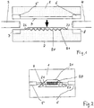
- the Bragg structure is substantially coarser in FIGS. 1 and 2 and the thickness of the high-index layer is exaggerated in FIG. 1.
- the embodiment according to FIG. 1 consists of a substrate 1 and a cover 2, which preferably consist of a polymer with a refractive index that corresponds to that of the cladding of the glass fibers 3, 4.
- a cover 2 which preferably consist of a polymer with a refractive index that corresponds to that of the cladding of the glass fibers 3, 4.
- fiber guide grooves 5, 6, 7, 8 are provided in the substrate 1 and in the cover 2.
- a part 10 of an injection mold made of metal is shown, which is the negatives for the fiber guide grooves 15, 16 and the groove for the waveguide 19 comprises, so that said structure is formed during injection molding.
- an adhesive is applied to the substrate, which has a higher refractive index than the substrate and serves both as a waveguide in the groove 9 and for the permanent connection of the substrate to a cover.
- This is shown schematically in FIG. 4 using a substrate 17 with three grooves 9, 9 'and 9''for waveguides.
- the glass fibers 3, 3 ', 3''and 4, 4', 4 '' are initially held by schematically illustrated preliminary holders 11, 12 and inserted into the fiber guide grooves.
- the cover 14 After the application of the adhesive 13, the cover 14 is pressed onto the substrate 17 with great pressure, so that the adhesive penetrates into the grooves 9, 9 ', 9' 'and fills them. Furthermore, the adhesive 13 penetrates into the parts of the fiber guide grooves which are not occupied by the glass fibers and thus fixes the glass fibers. The remaining adhesive is distributed over the surface of the substrate 17. The layer thickness of the adhesive is kept as low as possible by appropriate pressure. After the adhesive has hardened, the cover 14 is firmly connected to the substrate 17.
- the cover 2 (FIGS. 1 and 2) is provided with a Bragg structure 20.
- a Bragg structure 20 This can be done with a suitable molding process - for example, by injection molding in a form having the Bragg structure or by embossing with a suitable stamp.
- An optical layer 21 is applied to the Bragg structure 20, the refractive index of which lies above that of the adhesive, that is to say the waveguide, and which is therefore referred to below as a high-index layer.
- An advantageous value of the refractive index for the layer 21 is 1.53 with a refractive index of 1.48 of the substrate and 1.485 of the waveguide.
- the high refractive index layer should have only slight optical losses and should have a thickness of approximately 0.1 ⁇ m to 1 ⁇ m.
- care must be taken that the waveguide is operated in the single-mode range. This is the case, for example, with a layer thickness of 0.1 ⁇ m and a refractive index of 1.53.
- the high-index layer 21 increases the effect of the Bragg structure 20. All the surfaces provided with Bragg structures are covered with the high-index layer. To avoid an abrupt impact in the waveguide Integrated optical circuit, it is advantageous if the waveguide coming from the fiber connection continuously merges into the waveguide part covered with the thin, high-index layer.
- the continuous transition can be achieved by suitable shaping of the high-index layer in that the edges 22, 23 of the high-index layer 21 run in the direction of the fiber guide grooves 7, 8 such that they form an acute angle ⁇ with the waveguide. It can also be provided that the thickness of the high-index layer gradually increases from the edges 22, 23.
- the surface of the high-index layer 21 is flat, so that the thickness of the high-index layer 21 changes according to the Bragg structure. This creates a modulation of the refractive index, which is effective on the light wave guided in the waveguide. This further increases the effect of the Bragg structure.
- a layer can advantageously be applied by spray, dip or spin coating.
- the Bragg structure 20 it is also possible within the scope of the invention to apply a uniformly thick layer to the Bragg structure 20. This can be done, for example, by plasma deposition, sputtering processes or by laser-assisted chemical vapor disposition (laser CVD).
- laser CVD laser-assisted chemical vapor disposition
- the high-index layer 21 is a material provided for the high-index layer 21.
- Suitable materials for the high-index layer are inorganic dielectrics, such as Al2O3, Si3N4, SiONH or silicon-rich silicon nitride.
- the high-index layer 21 can be made of an organic dielectric, in particular polymer, or an inorganic-organic polymer (Ormocer) are formed. These materials are particularly suitable for application by a coating process in the liquid state.
- the high-index layer 21 is to locally increase the refractive index of the lid, which is made of polymer, by UV radiation, ion diffusion or implantation methods.
- the diffusion of suitable monomers from the gas phase can also raise the refractive index of the polymer cover plate in the desired manner.
- the lid itself can be subjected to this treatment or a thin photopolymerizable film can be applied and then photopolymerized by suitable irradiation.
Landscapes
- Physics & Mathematics (AREA)
- General Physics & Mathematics (AREA)
- Optics & Photonics (AREA)
- Engineering & Computer Science (AREA)
- Microelectronics & Electronic Packaging (AREA)
- Optical Integrated Circuits (AREA)
Applications Claiming Priority (2)
| Application Number | Priority Date | Filing Date | Title |
|---|---|---|---|
| DE4231113A DE4231113A1 (de) | 1992-09-17 | 1992-09-17 | Integriert optische Schaltung mit einer Bragg-Struktur |
| DE4231113 | 1992-09-17 |
Publications (2)
| Publication Number | Publication Date |
|---|---|
| EP0589268A1 true EP0589268A1 (fr) | 1994-03-30 |
| EP0589268B1 EP0589268B1 (fr) | 1998-04-22 |
Family
ID=6468178
Family Applications (1)
| Application Number | Title | Priority Date | Filing Date |
|---|---|---|---|
| EP93114216A Expired - Lifetime EP0589268B1 (fr) | 1992-09-17 | 1993-09-04 | Circuit optique integré avec une structure de Bragg |
Country Status (2)
| Country | Link |
|---|---|
| EP (1) | EP0589268B1 (fr) |
| DE (2) | DE4231113A1 (fr) |
Cited By (6)
| Publication number | Priority date | Publication date | Assignee | Title |
|---|---|---|---|---|
| EP0682276A1 (fr) * | 1994-05-12 | 1995-11-15 | Fujitsu Limited | Structure de connexion guide d'ondes-fibre optique et procédé de connexion guide d'ondes-fibre optique |
| EP0807836A3 (fr) * | 1996-05-14 | 1997-12-17 | Robert Bosch Gmbh | Procédé de fabrication d'un composant guide d'ondes integré et arrangement |
| WO1998058284A1 (fr) * | 1997-06-17 | 1998-12-23 | Harting Elektro-Optische Bauteile Gmbh & Co. Kg | Procede de fabrication d'un composant a fibre optique integree |
| WO2000046620A1 (fr) * | 1999-02-04 | 2000-08-10 | INSTITUT FüR MIKROTECHNIK MAINZ GMBH | Connecteur lenticulaire pour realiser des systemes optiques a jet libre pour plusieurs fibres optiques |
| JP2002139638A (ja) * | 2000-08-23 | 2002-05-17 | Matsushita Electric Ind Co Ltd | 光学素子及びその製造方法 |
| EP1182472A3 (fr) * | 2000-08-23 | 2004-02-04 | Matsushita Electric Industrial Co., Ltd. | Elément optique et procédé de sa fabrication |
Citations (5)
| Publication number | Priority date | Publication date | Assignee | Title |
|---|---|---|---|---|
| US4636031A (en) * | 1983-10-28 | 1987-01-13 | Chevron Research Company | Process of tuning a grated optical fiber and the tuned optical fiber |
| JPS63106605A (ja) * | 1986-10-24 | 1988-05-11 | Hitachi Ltd | 薄膜導波路型光回折素子 |
| WO1988008548A1 (fr) * | 1987-04-28 | 1988-11-03 | British Telecommunications Public Limited Company | Dispostif optique |
| US4923271A (en) * | 1989-03-28 | 1990-05-08 | American Telephone And Telegraph Company | Optical multiplexer/demultiplexer using focusing Bragg reflectors |
| EP0451047A1 (fr) * | 1990-04-03 | 1991-10-09 | Commissariat A L'energie Atomique | Composant optique intégré protégé contre l'environnement et son procédé de fabrication |
-
1992
- 1992-09-17 DE DE4231113A patent/DE4231113A1/de not_active Withdrawn
-
1993
- 1993-09-04 DE DE59308431T patent/DE59308431D1/de not_active Expired - Fee Related
- 1993-09-04 EP EP93114216A patent/EP0589268B1/fr not_active Expired - Lifetime
Patent Citations (5)
| Publication number | Priority date | Publication date | Assignee | Title |
|---|---|---|---|---|
| US4636031A (en) * | 1983-10-28 | 1987-01-13 | Chevron Research Company | Process of tuning a grated optical fiber and the tuned optical fiber |
| JPS63106605A (ja) * | 1986-10-24 | 1988-05-11 | Hitachi Ltd | 薄膜導波路型光回折素子 |
| WO1988008548A1 (fr) * | 1987-04-28 | 1988-11-03 | British Telecommunications Public Limited Company | Dispostif optique |
| US4923271A (en) * | 1989-03-28 | 1990-05-08 | American Telephone And Telegraph Company | Optical multiplexer/demultiplexer using focusing Bragg reflectors |
| EP0451047A1 (fr) * | 1990-04-03 | 1991-10-09 | Commissariat A L'energie Atomique | Composant optique intégré protégé contre l'environnement et son procédé de fabrication |
Non-Patent Citations (2)
| Title |
|---|
| 'Integrated Photonics Research' A. NEYER et al.: 'New Fabrication Technology for Optical Waveguides' 1992, Conference Proceedings, * |
| PATENT ABSTRACTS OF JAPAN vol. 12, no. 354 (P - 761)<3201> 22 September 1988 (1988-09-22) * |
Cited By (10)
| Publication number | Priority date | Publication date | Assignee | Title |
|---|---|---|---|---|
| EP0682276A1 (fr) * | 1994-05-12 | 1995-11-15 | Fujitsu Limited | Structure de connexion guide d'ondes-fibre optique et procédé de connexion guide d'ondes-fibre optique |
| US5557695A (en) * | 1994-05-12 | 1996-09-17 | Fujitsu Limited | Waveguide-optical fiber connection structure and waveguide-optical fiber connection method |
| US5784509A (en) * | 1994-05-12 | 1998-07-21 | Fujitsu Limited | Waveguide-optical fiber connection structure and waveguide-optical fiber connection method |
| EP0940699A1 (fr) * | 1994-05-12 | 1999-09-08 | Fujitsu Limited | Structure de connexion guide d'ondes-fibre optique et procédé de connexion guide d'ondes-fibre optique, substrat de guide d'ondes pour utilisation dans connexion guide d'ondes-fibre optique et procédé de fabrication d'un substrat de guide d'ondes ainsi que fibre optique avec substrat de fibre pour utilisation dans connexion guide d'ondes-fibre optique |
| EP0807836A3 (fr) * | 1996-05-14 | 1997-12-17 | Robert Bosch Gmbh | Procédé de fabrication d'un composant guide d'ondes integré et arrangement |
| WO1998058284A1 (fr) * | 1997-06-17 | 1998-12-23 | Harting Elektro-Optische Bauteile Gmbh & Co. Kg | Procede de fabrication d'un composant a fibre optique integree |
| WO2000046620A1 (fr) * | 1999-02-04 | 2000-08-10 | INSTITUT FüR MIKROTECHNIK MAINZ GMBH | Connecteur lenticulaire pour realiser des systemes optiques a jet libre pour plusieurs fibres optiques |
| JP2002139638A (ja) * | 2000-08-23 | 2002-05-17 | Matsushita Electric Ind Co Ltd | 光学素子及びその製造方法 |
| EP1182472A3 (fr) * | 2000-08-23 | 2004-02-04 | Matsushita Electric Industrial Co., Ltd. | Elément optique et procédé de sa fabrication |
| US6826344B2 (en) | 2000-08-23 | 2004-11-30 | Matsushita Electric Industrial Co., Ltd. | Optical element and method of fabrication thereof |
Also Published As
| Publication number | Publication date |
|---|---|
| DE59308431D1 (de) | 1998-05-28 |
| DE4231113A1 (de) | 1994-03-24 |
| EP0589268B1 (fr) | 1998-04-22 |
Similar Documents
| Publication | Publication Date | Title |
|---|---|---|
| EP0622647B1 (fr) | Guide d'onde optique à substrat plan et son utilisation | |
| DE69425831T2 (de) | Organische optische komponenten und herstellung davon | |
| DE4434321C2 (de) | Optischer Wellenleiter mit einem Polymerkern und dessen Herstellungsverfahren | |
| DE69113346T2 (de) | Herstellungsverfahren für optische Wellenleiter durch eine Ionaustauschtechnik auf einem Glassubstrat. | |
| EP0911658B1 (fr) | Procédé de fabrication de structures de guide d'onde comprenant des composants optiques | |
| DE2245374A1 (de) | Mehrstufige integrierte wellenleiterstruktur und verfahren zu ihrer herstellung | |
| EP0718418A1 (fr) | Procédé de production d'une couche à gradient | |
| DE3520813A1 (de) | Verfahren zur herstellung eines integrierten optischen lichtwellenleiters | |
| DE19619353A1 (de) | Verfahren zur Herstellung eines integriert optischen Wellenleiterbauteiles sowie Anordnung | |
| DE69926844T2 (de) | Planare Lichtwellenschaltung | |
| EP1499490B1 (fr) | Procede pour creer des corps tridimensionnels ou des surfaces tridimensionnelles par rayonnement laser | |
| DE19810584A1 (de) | Verfahren zur Herstellung einer optischen Wellenleiter-Vorrichtung | |
| EP0559040A1 (fr) | Procédé de fabrication de composants optoélectroniques | |
| EP0883825B1 (fr) | Procede de production de composants optiques avec guides d'ondes optiques accouples, et composants optiques produits selon ce procede | |
| EP0589268B1 (fr) | Circuit optique integré avec une structure de Bragg | |
| DE4006863A1 (de) | Optisches wellenleiterbauelement und verfahren zum herstellen eines optischen wellenleiterbauelementes | |
| EP0509342B1 (fr) | Procédé de fabrication de structures en forme de coin | |
| DE2614871C3 (de) | Verfahren zur Herstellung von Dünnschicht-Lichtleiterstrukturen | |
| DE69227077T2 (de) | Wellenleiterherstellung durch Bestrahlung von Siliziumoxyd mit Elektronen | |
| DE4401219A1 (de) | Integriert optisches Bauelement und Verfahren zur Herstellung eines integriert optischen Bauelements | |
| DE2614859A1 (de) | Verfahren zur herstellung von lichtleiterstrukturen mit dazwischenliegenden elektroden | |
| DE4440981A1 (de) | Optisches Verbundbauelement vom Reflexionstyp | |
| DE112004000346T5 (de) | Passive Ausrichtung optischer Fasern mit optischen Elementen | |
| WO2026012852A1 (fr) | Procédé de fabrication d'une structure de guide d'ondes et structure de guide d'ondes | |
| EP0043475A1 (fr) | Procédé de fabrication d'un dispositif microoptique intégré pour application avec des fibres multimodes |
Legal Events
| Date | Code | Title | Description |
|---|---|---|---|
| PUAI | Public reference made under article 153(3) epc to a published international application that has entered the european phase |
Free format text: ORIGINAL CODE: 0009012 |
|
| AK | Designated contracting states |
Kind code of ref document: A1 Designated state(s): DE FR GB IT |
|
| 17P | Request for examination filed |
Effective date: 19940930 |
|
| 17Q | First examination report despatched |
Effective date: 19961018 |
|
| GRAG | Despatch of communication of intention to grant |
Free format text: ORIGINAL CODE: EPIDOS AGRA |
|
| GRAG | Despatch of communication of intention to grant |
Free format text: ORIGINAL CODE: EPIDOS AGRA |
|
| GRAH | Despatch of communication of intention to grant a patent |
Free format text: ORIGINAL CODE: EPIDOS IGRA |
|
| GRAH | Despatch of communication of intention to grant a patent |
Free format text: ORIGINAL CODE: EPIDOS IGRA |
|
| GRAA | (expected) grant |
Free format text: ORIGINAL CODE: 0009210 |
|
| AK | Designated contracting states |
Kind code of ref document: B1 Designated state(s): DE FR GB IT |
|
| ET | Fr: translation filed | ||
| REF | Corresponds to: |
Ref document number: 59308431 Country of ref document: DE Date of ref document: 19980528 |
|
| ITF | It: translation for a ep patent filed | ||
| GBT | Gb: translation of ep patent filed (gb section 77(6)(a)/1977) |
Effective date: 19980623 |
|
| PLBE | No opposition filed within time limit |
Free format text: ORIGINAL CODE: 0009261 |
|
| 26N | No opposition filed | ||
| REG | Reference to a national code |
Ref country code: GB Ref legal event code: IF02 |
|
| REG | Reference to a national code |
Ref country code: GB Ref legal event code: 732E |
|
| REG | Reference to a national code |
Ref country code: GB Ref legal event code: 732E |
|
| PGFP | Annual fee paid to national office [announced via postgrant information from national office to epo] |
Ref country code: GB Payment date: 20030820 Year of fee payment: 11 |
|
| PGFP | Annual fee paid to national office [announced via postgrant information from national office to epo] |
Ref country code: FR Payment date: 20030909 Year of fee payment: 11 |
|
| PGFP | Annual fee paid to national office [announced via postgrant information from national office to epo] |
Ref country code: DE Payment date: 20030911 Year of fee payment: 11 |
|
| REG | Reference to a national code |
Ref country code: FR Ref legal event code: TP |
|
| PG25 | Lapsed in a contracting state [announced via postgrant information from national office to epo] |
Ref country code: GB Free format text: LAPSE BECAUSE OF NON-PAYMENT OF DUE FEES Effective date: 20040904 |
|
| PG25 | Lapsed in a contracting state [announced via postgrant information from national office to epo] |
Ref country code: DE Free format text: LAPSE BECAUSE OF NON-PAYMENT OF DUE FEES Effective date: 20050401 |
|
| GBPC | Gb: european patent ceased through non-payment of renewal fee |
Effective date: 20040904 |
|
| PG25 | Lapsed in a contracting state [announced via postgrant information from national office to epo] |
Ref country code: FR Free format text: LAPSE BECAUSE OF NON-PAYMENT OF DUE FEES Effective date: 20050531 |
|
| REG | Reference to a national code |
Ref country code: FR Ref legal event code: ST |
|
| PG25 | Lapsed in a contracting state [announced via postgrant information from national office to epo] |
Ref country code: IT Free format text: LAPSE BECAUSE OF NON-PAYMENT OF DUE FEES Effective date: 20050904 |