EP0589593A2 - Prélèvement électro-optique - Google Patents
Prélèvement électro-optique Download PDFInfo
- Publication number
- EP0589593A2 EP0589593A2 EP93307103A EP93307103A EP0589593A2 EP 0589593 A2 EP0589593 A2 EP 0589593A2 EP 93307103 A EP93307103 A EP 93307103A EP 93307103 A EP93307103 A EP 93307103A EP 0589593 A2 EP0589593 A2 EP 0589593A2
- Authority
- EP
- European Patent Office
- Prior art keywords
- probe
- electro
- optic
- crystal
- layer
- Prior art date
- Legal status (The legal status is an assumption and is not a legal conclusion. Google has not performed a legal analysis and makes no representation as to the accuracy of the status listed.)
- Ceased
Links
- 238000005070 sampling Methods 0.000 title claims abstract description 44
- 239000000523 sample Substances 0.000 claims abstract description 112
- 239000013078 crystal Substances 0.000 claims abstract description 46
- 239000010408 film Substances 0.000 claims abstract description 11
- 239000010409 thin film Substances 0.000 claims abstract description 6
- 229910001218 Gallium arsenide Inorganic materials 0.000 claims description 21
- 230000003287 optical effect Effects 0.000 claims description 19
- 239000000758 substrate Substances 0.000 claims description 16
- 239000011248 coating agent Substances 0.000 claims description 15
- 238000000576 coating method Methods 0.000 claims description 15
- 238000000034 method Methods 0.000 claims description 14
- 230000000694 effects Effects 0.000 claims description 4
- 230000005693 optoelectronics Effects 0.000 claims description 4
- 238000000151 deposition Methods 0.000 claims 3
- 238000005530 etching Methods 0.000 claims 2
- 239000000853 adhesive Substances 0.000 claims 1
- 230000001070 adhesive effect Effects 0.000 claims 1
- 239000006117 anti-reflective coating Substances 0.000 claims 1
- 230000003667 anti-reflective effect Effects 0.000 claims 1
- 238000007493 shaping process Methods 0.000 claims 1
- 229910012463 LiTaO3 Inorganic materials 0.000 abstract description 18
- 230000005540 biological transmission Effects 0.000 abstract description 6
- 230000035945 sensitivity Effects 0.000 abstract description 6
- 229910000980 Aluminium gallium arsenide Inorganic materials 0.000 description 21
- 239000004020 conductor Substances 0.000 description 13
- 239000000463 material Substances 0.000 description 7
- 230000005284 excitation Effects 0.000 description 6
- 238000005259 measurement Methods 0.000 description 5
- 235000012431 wafers Nutrition 0.000 description 5
- 238000002310 reflectometry Methods 0.000 description 4
- 239000011521 glass Substances 0.000 description 3
- 238000001451 molecular beam epitaxy Methods 0.000 description 3
- 230000010287 polarization Effects 0.000 description 3
- 238000005498 polishing Methods 0.000 description 3
- 238000012360 testing method Methods 0.000 description 3
- RTAQQCXQSZGOHL-UHFFFAOYSA-N Titanium Chemical compound [Ti] RTAQQCXQSZGOHL-UHFFFAOYSA-N 0.000 description 2
- 230000008859 change Effects 0.000 description 2
- 230000005684 electric field Effects 0.000 description 2
- 238000004519 manufacturing process Methods 0.000 description 2
- 238000012986 modification Methods 0.000 description 2
- 230000004048 modification Effects 0.000 description 2
- 230000004044 response Effects 0.000 description 2
- VYPSYNLAJGMNEJ-UHFFFAOYSA-N silicon dioxide Inorganic materials O=[Si]=O VYPSYNLAJGMNEJ-UHFFFAOYSA-N 0.000 description 2
- 230000001360 synchronised effect Effects 0.000 description 2
- 229910052719 titanium Inorganic materials 0.000 description 2
- 239000010936 titanium Substances 0.000 description 2
- 238000010521 absorption reaction Methods 0.000 description 1
- 238000004026 adhesive bonding Methods 0.000 description 1
- 230000008878 coupling Effects 0.000 description 1
- 238000010168 coupling process Methods 0.000 description 1
- 238000005859 coupling reaction Methods 0.000 description 1
- 238000001514 detection method Methods 0.000 description 1
- 239000006185 dispersion Substances 0.000 description 1
- 230000009977 dual effect Effects 0.000 description 1
- 230000005669 field effect Effects 0.000 description 1
- 239000005350 fused silica glass Substances 0.000 description 1
- 238000005286 illumination Methods 0.000 description 1
- 230000003993 interaction Effects 0.000 description 1
- 238000004943 liquid phase epitaxy Methods 0.000 description 1
- 230000003647 oxidation Effects 0.000 description 1
- 238000007254 oxidation reaction Methods 0.000 description 1
- 239000012071 phase Substances 0.000 description 1
- 230000010363 phase shift Effects 0.000 description 1
- 238000012545 processing Methods 0.000 description 1
- 239000010453 quartz Substances 0.000 description 1
- 230000005855 radiation Effects 0.000 description 1
- 239000004065 semiconductor Substances 0.000 description 1
- 230000003068 static effect Effects 0.000 description 1
- 239000012780 transparent material Substances 0.000 description 1
- 230000000007 visual effect Effects 0.000 description 1
Images



Classifications
-
- G—PHYSICS
- G01—MEASURING; TESTING
- G01R—MEASURING ELECTRIC VARIABLES; MEASURING MAGNETIC VARIABLES
- G01R1/00—Details of instruments or arrangements of the types included in groups G01R5/00 - G01R13/00 and G01R31/00
- G01R1/02—General constructional details
- G01R1/06—Measuring leads; Measuring probes
- G01R1/067—Measuring probes
- G01R1/07—Non contact-making probes
- G01R1/071—Non contact-making probes containing electro-optic elements
Definitions
- This invention pertains to electro-optic sampling of fast electronic and opto-electronic devices and circuits.
- Two-dimensional circuits have an open electrode structure which gives rise to fringing fields above the surface of the circuit.
- External electro-optic (e-o) probing techniques exploit the fringing fields to electro-optically sample fast electronic and opto-electronic devices and circuits.
- An e-o crystal probe placed into the fringing fields changes the crystal birefringence of the probe, which can then be measured optically by means of a pulsed light beam which is passed through the e-o crystal and is reflected from the circuit.
- Such external probes can be applied to almost any type of circuit, because the interaction is based on the field effect. Since no charge is removed from the circuit, the probe does not need to make an electrical contact to the circuit.
- FIGS. 6 and 7 a typical prior-art arrangement, 10, being used for optical sampling of an exemplary circuit having a plurality of conductors, 12, on a surface of a semiconductor substrate,13.
- the substrate and conductors are part of an integrated circuit.
- An electro-optic (e-o) crystalline probe 15 is mounted on a transparent support, 16, forming a supported probe, 14.
- An end face of probe 15 is positioned over or on the conductor whose voltage waveform is to be sampled. Sampling is performed optically by short-duration pulses of a polarized light beam 17 which is directed through support 16 into probe 14.
- Beam 17 is typically reflected from the conductor itself, but it may also be reflected by an optional reflector 18 (shown in dashed line in FIG. 6) disposed on the end face of the probe. The latter may be desirable in cases where the circuit is sensitive to light.
- the e-o crystal of probe 15 comprises a material which exhibits a longitudinal e-o effect; that is, a field-induced birefringence in response only to electric field components parallel to the direction of beam 17. Since the beam is directed perpendicularly to the surface of the conductor, only field components perpendicular to that surface induce the desired birefringence. The material itself need not have an inherent birefringence.
- Sampling pulses are generated by a pulsed laser 19, such as the well-known balanced colliding pulse mode-locked (CPM) dye laser or a passively mode-locked titanium doped sapphire laser, and are directed into the sampling apparatus via a microscope objective 21.
- Probe 14 is mounted optically (not physically) between crossed polarizers 22 and 23 and below a dichroic beam splitter 24 in such a way as to facilitate viewing of the end face of the probe from above via a microscope system 25.
- Incoherent white light is injected from an illumination source 26 through beam splitter 24 to illuminate the conductor below the probe. In this way, both the conductor and the sampling beam spot can be seen together.
- Quartz compensating plates 27 are included between polarizers 22 and 23 to operate the e-o crystal at a "zero-order" quarter wave point.
- Polarizer 23 which is a polarizing analyzer, is used to separate orthogonal polarizations and direct the output to dual differential light detectors 28 and 29. The detector output is then fed to a lock-in amplifier and signal averager, 30. The probe is then brought down to any suitable point on or above substrate 13 for sampling the voltage waveform of a selected conductor.
- a voltage waveform may be generated on the conductor by coupling a test signal thereto (or to the circuit of which it is a part) either electrically via a suitable (e.g. high-speed) electrical connection 31 or optically via optical delay line 32 coupled to a photodetector (not shown) on substrate 13.
- a suitable electrical connection 31 or optically via optical delay line 32 coupled to a photodetector (not shown) on substrate 13.
- well-known sampling techniques are utilized so that the optical pulses and the waveform being measured are synchronized, and the optical pulses are scanned across the waveform to be sampled.
- polarized beam 17 is illustratively used to sense change in the birefringence induced in the e-o crystal.
- the reflected beam (immediately before polarizer 23) has orthogonal polarization components which are 90 degrees out of phase with one another. These components are separated by the polarizing analyzer (polarizer 23) and generate equal signals (balanced outputs) from detectors 28 and 29.
- the birefringence induced in the crystal is changed, and an additional phase shift is produced between the two orthogonal components; i.e., the reflected beam is elliptically polarized, resulting in an imbalanced output from detectors 28 and 29 and a signal from lock-in amplifier/averager 30 which is proportional to the voltage on the conductor.
- the prior-art crystal probe 15 comprises a relatively thick slice of LiTaO3, e.g., about 100 ⁇ m thick, and the support 16 is a transparent material such as fused silica rod bonded to the probe.
- the probe and a portion of the rod adjacent to the LiTaO3 slice are polished as a four-sided pyramid having a half angle of about 30 degrees with the end face of the probe being 200 ⁇ m or less on a side. Deviations from 30° result in reduced facet reflectivities.
- the optic axis of the LiTaO3 is essentially perpendicular to the end face of the probe. If needed, an optional high reflecting (HR) coating 18 (FIG.
- HR high reflecting
- Microscope objective 21 is used both to focus the sampling beam onto the end face of the probe and to recollimate the reflected beam.
- Conductors 12 on substrate 13 are energized via either a waveform synthesizer (not shown) coupled to high-speed connection 31 and synchronized with the laser or vice-versa by frequency locking the laser to a master RF source or via an electrical signal from a photodetector (not shown) illuminated by the laser pulses from delay line 32.
- Electrical connections to the circuit may be made by conventional probes, a probe card, or wire bonding. Relative delay between trigger and sampling times is introduced by the motor driven optical delay line 32, although purely electronic means, in some cases, can also be utilized. Utilizing apparatus of this type with optical pulses of about 100fs duration, it is expected that measurement bandwidths in excess of 1 THz (1000 GHz) can be attained.
- the measured electrical rise times are often longer than the optical pulses. This difference is due in part to the distance the electrical signal must travel from the excitation site to the sampling site, and in part to the distance the optical sampling pulse must travel through the LiTaO3 sampling crystal. As the electrical pulse travels along the transmission line it is dispersed, resulting in preferential attenuation and radiation of the high frequency components. As the optical pulse travels in the LiTaO3 crystal it propagates with the electrical pulse, but at a different velocity. This results in velocity walk-off, causing the detected signal to appear longer. This walk-off effect becomes enhanced as the crystal thickness is increased.
- This invention embodies a new electro-optic sampling probe with femtosecond resolution suitable for ultra-fast electro-optic sampling.
- the new probe is several times thinner and has a dielectric constant four times less than the best reported conventional bulk LiTaO3 probes. In addition, the ultimate bandwidth is 50 percent greater than an equivalent LiTaO3 probe.
- the probe is a thin film of Al x Ga 1-x As used in both total internally reflecting and free-standing geometries. Here x is chosen for sufficient transmission of the crystal to the wavelength of the laser source being used for electro-optic sampling.
- the thickness of the film is a small fraction of the thickness of prior art probes and is chosen, for speed and sensitivity of electro-optic sampling, to be thin compared to the spatial extent of the laser pulse.
- the thin film probe eliminates many of the problems associated with the use of bulk crystals as electro-optic sensors.
- This invention embodies an electro-optic crystal probe for use with the e-o sampling system of the type described above.
- the probe may be utilized as a crystal film supported on a transparent rod (FIGS. 1 and 3) or as a free-standing probe (FIG. 4).
- the probe consists of a thin Al x Ga 1-x As layer (hereinafter referred to as AlGaAs).
- x is that fraction of Al in the AlGaAs crystal which is needed for sufficient transmission of the crystal to the wavelength of the laser source being used in the electro-optic sampling.
- the crystal probe is much thinner than the spatial extent of the optical pulse of a laser being used. For example, if a wavelength of a 100 fs optical pulse is 30 ⁇ m long in air, the thickness of the probe is selected to be thinner than this wavelength.
- the probe is fabricated using molecular beam epitaxy (MBE) to achieve an active layer which is thinner and more uniform than that achievable through polishing of bulk (e.g., LiTaO3 ) crystals.
- MBE molecular beam epitaxy
- the probe was grown as a thin layer or film on a (110) GaAs substrate wafer by molecular beam epitaxy.
- Use of a (110) GaAs substrate places the optical axis in the plane of the wafer.
- the layer is then removed from the substrate using selective etches.
- the thickness of the probe layer is chosen to be thinner than the spatial extent of the optical pulse of a laser being used. For CPM laser, the probe layer is about 7 ⁇ m thick. Thicker crystals can be fabricated by either MBE or other epitaxial growth techniques such as Liquid Phase Epitaxy.
- the Al content, or required band gap energy of the active layer is determined by the wavelength of the particular laser source used. For the case of the CPM laser, this laser requires the use of Al 0.8 Ga 0.2 As. On the other hand, a passively mode-locked titanium doped sapphire laser source would require less Al, since it operates at a longer wavelength. The requirement for a particular application is the relative absorption at the wavelength of the laser source being used.
- band gap engineering can be used for other III/V material systems, such as InP, and also for II/IV materials systems, such as CdS, since all of these materials have birefringent properties.
- the same crystalline layer may be fabricated into total internal reflecting geometries (either critical angle type, or through the use of a high reflective coating) or free-standing geometries.
- the supported probe 14 shown in FIG. 1 was prepared by gluing a small piece of GaAs wafer with a thin AlGaAs layer thereon to a glass rod or block 16 and polishing the probe and the adjacent end portion of the rod to a pyramidal shape, such that the glass/AlGaAs interface is of an appropriate size.
- appropriate size is meant a size of the probe constrained by the visual limitations of the microscope to be used in the sampling measurement, i.e., the AlGaAs crystal and the adjacent facets of the support rod must all be within the field of view if the sampling beam is to be routed as shown in FIG. 1.
- the interface is of the order of ⁇ 200 ⁇ m or less on a side.
- the GaAs substrate is then etched away leaving the thin AlGaAs layer attached to the glass support.
- This technique produces thinner crystal wafers, with better interface planarity than conventional polishing.
- a flat bottom element allows the probe to be interferometrically aligned on the sample. Parallelism on the order of a single fringe is routinely achieved.
- This fabrication technique enables the production of a Total Internal Reflection (TIR) probe geometry, which does not require the high reflection coating.
- TIR Total Internal Reflection
- the electrode geometry is a coplanar strip transmission line with 5 ⁇ m lines and spacings.
- the TIR geometry consisted of a simple multi-line system with no contact pads within the time window.
- Probe 15 was used on samples on LT-GaAs substrates producing electrical pulses ⁇ 1 ps FWHM.
- Sampling beam 17 is directed so that it impinges upon a facet of the pyramid, is directed to a point in crystal probe 15, and is reflected toward the microscope objective 21.
- excitation beam 32' is directed as is shown in dashed lines in FIG. 6 and impinges at about the same point as the sampling beam.
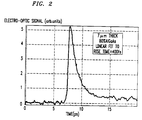
- FIG. 2 shows the measured response.
- a linear fit to the rise time (10-90 percent) in FIG. 2 is ⁇ 400 fs.
- FIG. 3 is shown a variant of supported probe 14.
- the free surface of crystal probe 15 is supported on rod 16 and is coated with an HR coating, 18; however, the sides of the support rod and the crystal probe do not need to be shaped.
- excitation beam 32' does not need to pass through the crystals as was the case in FIG. 1, but may be directed at a different portion of the circuit.
- FIG. 4 is shown an arrangement with a free-standing probe, 31.
- the probe is approximately 7 ⁇ m thick and is provided with an Anti-Reflectivity (AR) coating, 33, which is applied to the top of the probe and a High-Reflectivity (HR) coating, 18, applied to the bottom of the probe.
- AR Anti-Reflectivity
- HR High-Reflectivity
- the sampling beam is reflected from the HR coating.
- the excitation beam 32 (not shown) is 2-3 optical beam diameters away from sampling beam 17, resulting in a propagation distance of approximately 15 ⁇ m. The reflections are assumed to be caused by nearby contact pads.
- This probe is produced by growing an AlGaAs film on a GaAs substrate wafer, in the manner similar to the growth of the probe for the variant shown in FIG. 1. However, here the top surface of the AlGaAs film is AR coated, and the substrate is then chemically removed using a preferential etch which produces large area ( ⁇ 1cm2) free-standing films.
- HR coating, 18, is applied to the back of the AlGaAs film, which is the lateral plane of the film opposite to the AR-coated side. If a particular HR coating used does not produce a high reflectivity, an Au electrode on the sample may be used as an additional mirror. This may be accomplished simply by moving the probe so that sampling beam 17 is over the surface of electrode 12.
- an in-line photoconductive switch with a 5 ⁇ m gap is located 100 ⁇ m from a side sampling gate.
- the side sampling gate is the third electrode shown in FIG. 4, grounded in this configuration. This makes the coplanar transmission line look like a three-line system at the sampling site.
- Table 1 of the Appendix shows a comparison of physical constants of AlGaAs and of other probe materials typically used for fast electro-optic sampling (LiTaO3 and GaAs).
- the dielectric constant of LiTaO3 is very large, resulting in large signal dispersion for any significant propagation distance inside the crystal.
- GaAs has a better voltage sensitivity than LiTaO3, it cannot be used with most femtosecond laser systems (the band edge of GaAs is >850 nm).
- the AlGaAs probe offers a reasonable electro-optic coefficient, but has a lower dielectric constant than either LiTaO3 or GaAs.
- the probe used in this work is AlGaAs (80 percent Al), to minimize oxidation which takes place with pure AlAs. At this Al content, optical excitation is indirect.
- TO phonon is 45.26 meV or 10.86 THz.
- the corresponding TO phonon in GaAs is 8.032 THz.
- AlGaAs 1.0 ⁇ m
- AlGaAs is almost twice as sensitive as an equivalent GaAs modulator.
- the shorter propagation distance inside the crystal makes the total sensitivity less for a thinner crystal, as the integrated polarization change is a function of modulator length.
- High frequency detection techniques make sensitivity a less important issue for sampling applications of these modulators. Similar calculations and considerations may be applied to AlGaAs crystal probes with other than 0.8.
Landscapes
- Physics & Mathematics (AREA)
- General Physics & Mathematics (AREA)
- Testing Or Measuring Of Semiconductors Or The Like (AREA)
- Measurement Of Current Or Voltage (AREA)
- Photometry And Measurement Of Optical Pulse Characteristics (AREA)
- Tests Of Electronic Circuits (AREA)
- Investigating Or Analysing Materials By Optical Means (AREA)
Applications Claiming Priority (2)
| Application Number | Priority Date | Filing Date | Title |
|---|---|---|---|
| US948059 | 1992-09-21 | ||
| US07/948,059 US5406194A (en) | 1992-09-21 | 1992-09-21 | Alx Ga1-x as probe for use in electro-optic sampling |
Publications (2)
| Publication Number | Publication Date |
|---|---|
| EP0589593A2 true EP0589593A2 (fr) | 1994-03-30 |
| EP0589593A3 EP0589593A3 (fr) | 1995-03-08 |
Family
ID=25487194
Family Applications (1)
| Application Number | Title | Priority Date | Filing Date |
|---|---|---|---|
| EP93307103A Ceased EP0589593A3 (fr) | 1992-09-21 | 1993-09-09 | Prélèvement électro-optique. |
Country Status (6)
| Country | Link |
|---|---|
| US (1) | US5406194A (fr) |
| EP (1) | EP0589593A3 (fr) |
| JP (1) | JP3072814B2 (fr) |
| KR (1) | KR100311557B1 (fr) |
| CA (1) | CA2105270C (fr) |
| SG (1) | SG43950A1 (fr) |
Families Citing this family (14)
| Publication number | Priority date | Publication date | Assignee | Title |
|---|---|---|---|---|
| US5625617A (en) * | 1995-09-06 | 1997-04-29 | Lucent Technologies Inc. | Near-field optical apparatus with a laser having a non-uniform emission face |
| US6025911A (en) * | 1995-11-14 | 2000-02-15 | University Of New Mexico | Broadband ultrashort pulse measuring device using non-linear electronic components |
| JP3388319B2 (ja) * | 1996-05-31 | 2003-03-17 | レンセレー ポリテクニク インスティテュート | 自由空間の電磁放射を特徴づけるための電気光学及び磁気光学感知装置及び方法 |
| US6414473B1 (en) | 1996-05-31 | 2002-07-02 | Rensselaer Polytechnic Institute | Electro-optic/magneto-optic measurement of electromagnetic radiation using chirped optical pulse |
| US5952818A (en) * | 1996-05-31 | 1999-09-14 | Rensselaer Polytechnic Institute | Electro-optical sensing apparatus and method for characterizing free-space electromagnetic radiation |
| JP3223155B2 (ja) * | 1998-02-05 | 2001-10-29 | 科学技術振興事業団 | 薄膜スピンプローブ |
| JP4091214B2 (ja) * | 1999-06-10 | 2008-05-28 | 浜松ホトニクス株式会社 | テラヘルツ波分光器 |
| GB2371618B (en) * | 2001-01-30 | 2004-11-17 | Teraprobe Ltd | A probe, apparatus and method for examining a sample |
| US7844437B1 (en) * | 2001-11-19 | 2010-11-30 | Cypress Semiconductor Corporation | System and method for performing next placements and pruning of disallowed placements for programming an integrated circuit |
| US6977379B2 (en) * | 2002-05-10 | 2005-12-20 | Rensselaer Polytechnic Institute | T-ray Microscope |
| US20090020511A1 (en) * | 2007-07-17 | 2009-01-22 | Kommera Swaroop K | Ablation |
| WO2012101979A1 (fr) * | 2011-01-24 | 2012-08-02 | 株式会社村田製作所 | Sonde de champ électrique |
| KR20120087631A (ko) | 2011-01-28 | 2012-08-07 | 삼성전자주식회사 | 나노 구조화된 음향광학 소자, 및 상기 음향광학 소자를 이용한 광 스캐너, 광 변조기 및 홀로그래픽 디스플레이 장치 |
| WO2016140377A1 (fr) * | 2015-03-02 | 2016-09-09 | 한국전기연구원 | Sonde d'antenne à fente, et appareil et procédé permettant d'inspecter des défauts d'un semi-conducteur multijonction l'utilisant |
Citations (1)
| Publication number | Priority date | Publication date | Assignee | Title |
|---|---|---|---|---|
| US4681449A (en) * | 1984-09-07 | 1987-07-21 | Stanford University | High speed testing of electronic circuits by electro-optic sampling |
Family Cites Families (10)
| Publication number | Priority date | Publication date | Assignee | Title |
|---|---|---|---|---|
| US3614451A (en) * | 1968-08-19 | 1971-10-19 | Ibm | Sampling system utilizing electrooptic techniques |
| US4446425A (en) * | 1982-02-12 | 1984-05-01 | The University Of Rochester | Measurement of electrical signals with picosecond resolution |
| US4618819A (en) * | 1984-03-27 | 1986-10-21 | The University Of Rochester | Measurement of electrical signals with subpicosecond resolution |
| US4891580A (en) * | 1988-04-29 | 1990-01-02 | American Telephone And Telegraph Co., At&T Bell Laboratories | Electro-optic measurements of voltage waveforms on electrical conductors |
| US4873485A (en) * | 1988-07-13 | 1989-10-10 | The University Of Rochester | Electro-optic signal measurement |
| US5006789A (en) * | 1989-05-23 | 1991-04-09 | The University Of Rochester | Electro-optic signal measurement |
| US4928058A (en) * | 1989-05-23 | 1990-05-22 | The University Of Rochester | Electro-optic signal measurement |
| US4978910A (en) * | 1989-06-26 | 1990-12-18 | At&T Bell Laboratories | Electrooptic apparatus for the measurement of ultrashort electrical signals |
| US4923564A (en) * | 1989-08-24 | 1990-05-08 | American Telephone And Telegraph Company | Selective etching process |
| JPH03154875A (ja) * | 1989-11-13 | 1991-07-02 | Dainippon Printing Co Ltd | 電気光学結晶を用いた電位センサ及び電位測定方法 |
-
1992
- 1992-09-21 US US07/948,059 patent/US5406194A/en not_active Expired - Lifetime
-
1993
- 1993-08-31 CA CA002105270A patent/CA2105270C/fr not_active Expired - Fee Related
- 1993-09-03 JP JP05242132A patent/JP3072814B2/ja not_active Expired - Fee Related
- 1993-09-09 SG SG1996006765A patent/SG43950A1/en unknown
- 1993-09-09 EP EP93307103A patent/EP0589593A3/fr not_active Ceased
- 1993-09-20 KR KR1019930019064A patent/KR100311557B1/ko not_active Expired - Lifetime
Patent Citations (1)
| Publication number | Priority date | Publication date | Assignee | Title |
|---|---|---|---|---|
| US4681449A (en) * | 1984-09-07 | 1987-07-21 | Stanford University | High speed testing of electronic circuits by electro-optic sampling |
Non-Patent Citations (2)
| Title |
|---|
| "Electroluminescent Materials and Devices" * |
| "Schottky Diodes and Ohmic Contacts for the III-V Semiconductors. Pages 73 to 163 of Physics and Chemistry of III-V Compound Semiconductor Interfaces. Pages 123 to 128" * |
Also Published As
| Publication number | Publication date |
|---|---|
| JP3072814B2 (ja) | 2000-08-07 |
| SG43950A1 (en) | 1997-11-14 |
| US5406194A (en) | 1995-04-11 |
| JPH06224272A (ja) | 1994-08-12 |
| CA2105270A1 (fr) | 1994-03-22 |
| CA2105270C (fr) | 1998-07-28 |
| KR100311557B1 (ko) | 2001-12-15 |
| KR940008172A (ko) | 1994-04-29 |
| EP0589593A3 (fr) | 1995-03-08 |
Similar Documents
| Publication | Publication Date | Title |
|---|---|---|
| EP0160209B1 (fr) | Mesure de signaux électriques avec une résolution inférieure aux picosecondes | |
| US5406194A (en) | Alx Ga1-x as probe for use in electro-optic sampling | |
| US4618819A (en) | Measurement of electrical signals with subpicosecond resolution | |
| Thakur et al. | Single-pass thin-film electro-optic modulator based on an organic molecular salt | |
| US5864393A (en) | Optical method for the determination of stress in thin films | |
| EP0150752B1 (fr) | Modulateur électro-optique interférentiel à haute sensibilité | |
| CN100565099C (zh) | 用于提高光声膜厚度测量系统中的信噪比的方法和设备 | |
| US5850140A (en) | Electric field sensor having sensor head with unbalanced electric field shield to shield branched optical waveguides against an applied electric field | |
| CA1313223C (fr) | Mesures electro-optiques des formes d'ondes de tension sur des conducteurs electriques | |
| Valdmanis | Electro-optic measurement techniques for picosecond materials, devices, and integrated circuits | |
| US4910454A (en) | System for electrical signal sampling with ultrashort optical pulses | |
| EP0614520A1 (fr) | Detecteur de temperature birefringent. | |
| US4873485A (en) | Electro-optic signal measurement | |
| JPH083495B2 (ja) | 電気信号を光学的に測定するための機械式プローブ | |
| EP0357475A1 (fr) | Systèmes de mesure électrooptiques pour l'analyse fréquentielle de signaux à trés large bande | |
| JPH09211035A (ja) | 電界測定装置 | |
| Cheo | Electro‐optic properties of reverse‐biased GaAs epitaxial thin films at 10.6 μm | |
| Vickers et al. | Fabry–Pe´ rot enhancement of external electro-optic sampling | |
| Khalfallah et al. | A GaAlAs-GaAs integrated coherence modulator | |
| Chandani | Fiber-based probe for electrooptic sampling | |
| Zhang et al. | External electro-optic measurement utilizing poled polymer-based asymmetric Fabry–Perot reflection film | |
| KR920000565B1 (ko) | 전도체 전기 신호의 전압 파형 측정 방법 및 그 장치 | |
| JP3063369B2 (ja) | 磁界検出装置 | |
| JP2002257887A (ja) | 反射型電界センサヘッド及び反射型電界センサ | |
| JPH06342017A (ja) | 電界強度測定装置 |
Legal Events
| Date | Code | Title | Description |
|---|---|---|---|
| PUAI | Public reference made under article 153(3) epc to a published international application that has entered the european phase |
Free format text: ORIGINAL CODE: 0009012 |
|
| AK | Designated contracting states |
Kind code of ref document: A2 Designated state(s): DE FR GB |
|
| RAP3 | Party data changed (applicant data changed or rights of an application transferred) |
Owner name: AT&T CORP. |
|
| PUAL | Search report despatched |
Free format text: ORIGINAL CODE: 0009013 |
|
| AK | Designated contracting states |
Kind code of ref document: A3 Designated state(s): DE FR GB |
|
| 17P | Request for examination filed |
Effective date: 19950824 |
|
| 17Q | First examination report despatched |
Effective date: 19970606 |
|
| GRAG | Despatch of communication of intention to grant |
Free format text: ORIGINAL CODE: EPIDOS AGRA |
|
| STAA | Information on the status of an ep patent application or granted ep patent |
Free format text: STATUS: THE APPLICATION HAS BEEN REFUSED |
|
| 18R | Application refused |
Effective date: 20020602 |