EP0590191B1 - Anordnung zur Frequenzumsetzung - Google Patents
Anordnung zur Frequenzumsetzung Download PDFInfo
- Publication number
- EP0590191B1 EP0590191B1 EP92116745A EP92116745A EP0590191B1 EP 0590191 B1 EP0590191 B1 EP 0590191B1 EP 92116745 A EP92116745 A EP 92116745A EP 92116745 A EP92116745 A EP 92116745A EP 0590191 B1 EP0590191 B1 EP 0590191B1
- Authority
- EP
- European Patent Office
- Prior art keywords
- signal
- frequency
- transistor
- arrangement
- circuit
- Prior art date
- Legal status (The legal status is an assumption and is not a legal conclusion. Google has not performed a legal analysis and makes no representation as to the accuracy of the status listed.)
- Expired - Lifetime
Links
Images
Classifications
-
- H—ELECTRICITY
- H03—ELECTRONIC CIRCUITRY
- H03D—DEMODULATION OR TRANSFERENCE OF MODULATION FROM ONE CARRIER TO ANOTHER
- H03D7/00—Transference of modulation from one carrier to another, e.g. frequency-changing
- H03D7/12—Transference of modulation from one carrier to another, e.g. frequency-changing by means of semiconductor devices having more than two electrodes
- H03D7/125—Transference of modulation from one carrier to another, e.g. frequency-changing by means of semiconductor devices having more than two electrodes with field effect transistors
Definitions
- the invention relates to an arrangement for frequency conversion of an input signal of frequency f 1 with an oscillator signal of frequency f 2 to an intermediate frequency signal f 3 according to the preamble of claim 1.
- an input signal is generally used with an oscillator signal over a nonlinear Characteristic controlled in such a way that the mixing result u. a. the desired intermediate frequency signal arises.
- a nonlinear Characteristic controlled in such a way that the mixing result u. a. the desired intermediate frequency signal arises.
- the invention is based on the object of an arrangement Frequency conversion of the type mentioned at the outset with high intermodulation resistance with low power requirements to accomplish.
- the advantages achieved with the invention are in particular in that the intermodulation strength of the Overall arrangement is achieved.
- the input signal and the Intermediate frequency signal connections are low-impedance (50 ohms to 100 ohms) and unbalanced.
- the low power consumption is an advantage the arrangement, for example is only 300mW. It also becomes a big allowable Operating voltage range from approximately 2.5V to 7V and a large permissible L.O. (local oscillator) level range achieved for optimal operation.
- Another advantage the high stability of the arrangement, i.e. it does not occur Tendency to vibrate.
- the passive switch mixer stage also stands out due to low mixing losses. The order has a very high mixing efficiency.
- the mixer principle is applicable for frequencies from the LF range up to the high GHz range.
- the mixer is low noise.
- the mixer can be easily and without and / or output with amplifiers, transimpedance amplifiers be wired.
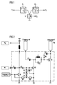
- FIG. 1 the function of the mixer of the arrangement is shown.
- or f 3
- the frequencies also stand for frequency bands.
- a switch element S preferably a field effect transistor, but also a diode etc., for example, is switched in parallel with the signal-carrying path with a control source of oscillator frequency f 2 with high and low resistance.
- a frequency-selective circuit F 1 and F 2 is inserted in each of the signal-supplying and signal-discharging parts of the signal-carrying path with the following properties: In the supplying path: passage for f 1 and blocking for f 3 . In the laxative path: passage for f 3 and blocking for f 1 .
- the blocking in the circuits F 1 and F 2 which are expediently designed as filters, takes place with high impedance in the direction of the switch element S and is symbolized in FIG. 1 by a reversing arrow.
- the overall circuit of the arrangement for frequency conversion shown in FIG. 2 comprises a mixer, a regulated LO driver amplifier and an IF amplifier, which are preferably monolithically integrated in a semiconductor substrate.
- the supplied LO level can be between -10dBm and + 13dBm (factor 200) without the function being significantly impaired.
- the operating voltage U B can vary in this circuit in a wide range between 2.5V and 7V.
- the achievable intermodulation distance of this mixer is 100 to 1000 times better than that of previously known MMIC mixers for consumer electronics.
- the mixer consists of the passive (without operating current working) mixer transistor Q2 and the frequency filters. This is in the RF path as the path to be signaled High-pass filter C3 and in the signal-discharging or IF path as Bandstop the inductance L1 and the capacitance C4.
- the Diode D1 protects the gate of the field effect transistor (mixer transistor Q2) before too high current densities in the direction of flow.
- the LO driver amplifier consists of transistor Q1, the high gain of which is achieved with a high slope due to a large gate width.
- the amplified LO signal controls the gate of the mixer transistor Q2 (switch operation) via C2.
- the sum of the capacitive loads on the drain of transistor Q2 is compensated for by an external inductance L, which takes into account the inductance of the housing connection.
- the capacitor C1 which can optionally be connected to the ground M, serves to reduce the external inductance L.
- the IF or IF amplifier consists of one with the resistor R3 resistance-coupled transistor Q3 to the Keep input and output low impedance (75 ohms to 100 ohms).
- the integrated DC isolation capacitor C5 can enlarged by an optional external capacitor with which the low-resistance input into the IF amplifier can be expanded to lower frequencies.
Landscapes
- Engineering & Computer Science (AREA)
- Power Engineering (AREA)
- Amplifiers (AREA)
- Superheterodyne Receivers (AREA)
Description
Es zeigen
- FIG 1
- eine Prinzipdarstellung der Schaltungsanordnung und
- FIG 2
- ein Scnaltungsbeispiel der Anordnung.
Die Summe der kapazitiven Belastungen am Drain des Transistors Q2 wird mit einer externen Induktivität L kompensiert, welche die Induktivität des Gehäuseanschlusses berücksichtigt. Der optional auf die Masse M anschließbare Kondensator C1 dient zur Verkleinerung der externen Induktivität L.
Claims (6)
- Anordnung zur Frequenzumsetzung eines Eingangssignals der Frequenz f1 mit einem Oszillatorsignal der Frequenz f2 zu einem Zwischenfrequenzsignal f3,dadurch gekennzeichnet, dass zwischen der Steuerquelle und dem Schalterelement (S) ein L.O.-Treiberverstärker (Q1) und eine Begrenzer- und Regelschaltung (D2,D3,D4;R1,R2) zur Begrenzung eines L.O.-Signals und zum Abregeln des L.O. Treiberverstärkers vorgesehen ist, sodaß das Schalterelement optimal angesteuert wird.bei der parallel zu einem signalführenden Pfad ein Schalterelement (S) geschaltet ist, das mit einer Steuerquelle der Oszillatorfrequenz f2 hoch- und niederohmig geschaltet wird, bei der in einem signalzuführenden Pfad des signalführenden Pfades eine frequenzselektive Schaltung (F1) eingefügt ist, mit den Eigenschaften, Durchlass für die Frequenz f1 und sperrung für die Frequenz f3 undbei der in einem signalabführenden Pfad des signalführenden Pfades eine weitere frequenzselektive Schaltung (F2) eingefügt ist, mit den Eigenschaften, Durchlass für die Frequenz f3 und Sperrung für die Frequenz f1,
- Anordnung gemäß Anspruch 1, dadurch gekennzeichnet, dass das Schalterelement (S) ein Mischertransistor (Q2), insbesondere ein Feldeffekttransistor ist.
- Anordnung gemäß Anspruch 1 oder 2, dadurch gekennzeichnet, dass der L.O.-Treiberverstärker einen Transistor (Q1) aufweist und dass die Begrenzer- und Regelschaltung drei seriell verschaltete Dioden (D2, D3, D4) und zwei Widerstände (R1, R2) aufweist, die im Betrieb der Anordnung einer-seits ein vom L.O.-Treiberverstärker verstärktes L.O.-Signal begrenzt und andererseits den Transistor (Q1) so abregelt, dass der Mischertransistor (Q2) optimal angesteuert wird und gleichzeitig eine Minimierung des Stromverbrauchs der Anordnung erreicht wird.
- Anordnung gemäß einem der Ansprüche 1 bis 3, dadurch gekennzeichnet, dass im signalabführenden Pfad ein ZF-Verstärker vorgesehen ist.
- Anordnung gemäß Anspruch 4, dadurch gekennzeichnet, dass der ZF-Verstärker einen widerstandsgegengekoppelten weiteren Transistor (Q3) aufweist.
- Anordnung nach einem der Ansprüche 1 bis 5, dadurch gekennzeichnet, dass die Anordnung auf einem Halbleitersubstrat monolithisch integriert ist.
Priority Applications (4)
| Application Number | Priority Date | Filing Date | Title |
|---|---|---|---|
| EP92116745A EP0590191B1 (de) | 1992-09-30 | 1992-09-30 | Anordnung zur Frequenzumsetzung |
| DE59209454T DE59209454D1 (de) | 1992-09-30 | 1992-09-30 | Anordnung zur Frequenzumsetzung |
| US08/118,225 US5465419A (en) | 1992-09-30 | 1993-09-09 | Arrangement for frequency conversion of an input signal with an oscillator signal to form an intermediate frequency signal |
| JP26835593A JP3442834B2 (ja) | 1992-09-30 | 1993-09-29 | 周波数変換装置 |
Applications Claiming Priority (1)
| Application Number | Priority Date | Filing Date | Title |
|---|---|---|---|
| EP92116745A EP0590191B1 (de) | 1992-09-30 | 1992-09-30 | Anordnung zur Frequenzumsetzung |
Publications (2)
| Publication Number | Publication Date |
|---|---|
| EP0590191A1 EP0590191A1 (de) | 1994-04-06 |
| EP0590191B1 true EP0590191B1 (de) | 1998-08-12 |
Family
ID=8210086
Family Applications (1)
| Application Number | Title | Priority Date | Filing Date |
|---|---|---|---|
| EP92116745A Expired - Lifetime EP0590191B1 (de) | 1992-09-30 | 1992-09-30 | Anordnung zur Frequenzumsetzung |
Country Status (4)
| Country | Link |
|---|---|
| US (1) | US5465419A (de) |
| EP (1) | EP0590191B1 (de) |
| JP (1) | JP3442834B2 (de) |
| DE (1) | DE59209454D1 (de) |
Families Citing this family (9)
| Publication number | Priority date | Publication date | Assignee | Title |
|---|---|---|---|---|
| EP0716500B1 (de) * | 1994-10-28 | 2000-07-05 | Murata Manufacturing Co., Ltd. | Mischer und Frequenzumsetzungsprozess unter Verwendung desselben |
| JP3227641B2 (ja) * | 1994-10-28 | 2001-11-12 | 株式会社村田製作所 | ミキサ回路および周波数変換方法 |
| US5678226A (en) * | 1994-11-03 | 1997-10-14 | Watkins Johnson Company | Unbalanced FET mixer |
| US5732345A (en) * | 1995-12-20 | 1998-03-24 | Watkins-Johnson Company | Quasi-double balanced dual-transformer dual FET mixer, which achieves better isolation by using a first and second diplexer, and a transmission line RF balun |
| US5697091A (en) * | 1996-02-07 | 1997-12-09 | Ford Motor Company | Distortion-free chopper-based signal mixer |
| JP3395704B2 (ja) | 1999-04-06 | 2003-04-14 | 松下電器産業株式会社 | 周波数変換装置 |
| US6665528B2 (en) * | 2000-06-07 | 2003-12-16 | Infineon Technologies North America Corp. | Dual band fet mixer |
| JP3853604B2 (ja) | 2001-04-04 | 2006-12-06 | 松下電器産業株式会社 | 周波数変換回路 |
| DE102004005031B4 (de) * | 2004-01-30 | 2020-09-03 | Sennheiser Electronic Gmbh & Co. Kg | Mikrofon-Empfänger |
Family Cites Families (6)
| Publication number | Priority date | Publication date | Assignee | Title |
|---|---|---|---|---|
| JPS5513512A (en) * | 1978-07-14 | 1980-01-30 | Hitachi Denshi Ltd | Frequency converter |
| FR2521784B1 (fr) * | 1982-02-12 | 1985-09-20 | Thomson Csf | Melangeur a transistor pour hyperfrequences |
| IT1183692B (it) * | 1985-05-24 | 1987-10-22 | Face Standard Ind | Miscelatore di segnali per apparati radio a micro-onde |
| BE902515A (fr) * | 1985-05-28 | 1985-11-28 | Saint Roch Glaceries | Ensemble a depression pour le maintien du verre notamment dans des machines de faconnage. |
| US5001776A (en) * | 1988-10-27 | 1991-03-19 | Motorola Inc. | Communication system with adaptive transceivers to control intermodulation distortion |
| US5083050A (en) * | 1990-11-30 | 1992-01-21 | Grumman Aerospace Corporation | Modified cascode mixer circuit |
-
1992
- 1992-09-30 DE DE59209454T patent/DE59209454D1/de not_active Expired - Lifetime
- 1992-09-30 EP EP92116745A patent/EP0590191B1/de not_active Expired - Lifetime
-
1993
- 1993-09-09 US US08/118,225 patent/US5465419A/en not_active Expired - Lifetime
- 1993-09-29 JP JP26835593A patent/JP3442834B2/ja not_active Expired - Lifetime
Also Published As
| Publication number | Publication date |
|---|---|
| EP0590191A1 (de) | 1994-04-06 |
| JPH06204751A (ja) | 1994-07-22 |
| US5465419A (en) | 1995-11-07 |
| JP3442834B2 (ja) | 2003-09-02 |
| DE59209454D1 (de) | 1998-09-17 |
Similar Documents
| Publication | Publication Date | Title |
|---|---|---|
| DE4410030C2 (de) | Rauscharmer, aktiver Mischer | |
| DE102007027047B4 (de) | Hochfrequenzleistungsverstärker | |
| DE69108466T2 (de) | Hochfrequenzleistungsverstärker mit hohem Wirkungsgrad. | |
| DE19534382B4 (de) | Monolithisch integrierte Schaltung mit einem Mikrowellen-Leistungsverstärker mit einer Anpassungsschaltung unter Verwendung verteilter Leitungen | |
| DE2219122A1 (de) | Feldeffekttransistorstufe, insbesondere als Mischer und HF-Verstärker mit verbesserter Intermodulationsunterdrückung | |
| DE10231181A1 (de) | Verstärkerschaltung mit einstellbarer Verstärkung und Sendeanordnung mit der Verstärkerschaltung | |
| DE69321565T2 (de) | HF-Verstärker mit veränderbarer Verstärkung und linearer Verstärkungssteuerung | |
| EP0590191A1 (de) | Anordnung zur Frequenzumsetzung | |
| DE69214923T2 (de) | Integrierte Schaltung mit einem Verstärker mit variabler Verstärkung | |
| DE10344876B3 (de) | Signalverarbeitungseinrichtung, insbesondere für den Mobilfunk | |
| DE60131542T2 (de) | Rausch- und eingangsimpedanzangepasster verstärker | |
| DE4331499C2 (de) | Spannungsgesteuerter Oszillator | |
| DE60101089T2 (de) | Multifunktionelle integrierte schaltungsanordnung hoher frequenz | |
| DE19501236C2 (de) | Verstärker | |
| DE69613628T2 (de) | Eingangsschaltung | |
| DE3210453C2 (de) | Signal-Eingangsschaltung | |
| DE102008011629B4 (de) | Verstärker | |
| DE19642900C2 (de) | Mischerschaltung | |
| DE102005032093B9 (de) | Verstärkeranordnung | |
| DE1261191B (de) | Mischschaltung | |
| DE3246295C2 (de) | Frequenzmodulierbarer Oszillator | |
| DE10214724A1 (de) | Frequenzwandelschaltung | |
| DE69518968T2 (de) | Hochfrequenzverstärkungsschaltung | |
| DE19536431C1 (de) | Integrierter Mikrowellen-Silizium-Baustein | |
| DE102005040489A1 (de) | Halbleiter-IC |
Legal Events
| Date | Code | Title | Description |
|---|---|---|---|
| PUAI | Public reference made under article 153(3) epc to a published international application that has entered the european phase |
Free format text: ORIGINAL CODE: 0009012 |
|
| AK | Designated contracting states |
Kind code of ref document: A1 Designated state(s): AT BE CH DE DK ES FR GB GR IE IT LI LU MC NL PT SE |
|
| RBV | Designated contracting states (corrected) |
Designated state(s): DE FR NL |
|
| 17P | Request for examination filed |
Effective date: 19940920 |
|
| 17Q | First examination report despatched |
Effective date: 19960725 |
|
| GRAG | Despatch of communication of intention to grant |
Free format text: ORIGINAL CODE: EPIDOS AGRA |
|
| GRAG | Despatch of communication of intention to grant |
Free format text: ORIGINAL CODE: EPIDOS AGRA |
|
| GRAH | Despatch of communication of intention to grant a patent |
Free format text: ORIGINAL CODE: EPIDOS IGRA |
|
| GRAH | Despatch of communication of intention to grant a patent |
Free format text: ORIGINAL CODE: EPIDOS IGRA |
|
| GRAA | (expected) grant |
Free format text: ORIGINAL CODE: 0009210 |
|
| AK | Designated contracting states |
Kind code of ref document: B1 Designated state(s): DE FR NL |
|
| REF | Corresponds to: |
Ref document number: 59209454 Country of ref document: DE Date of ref document: 19980917 |
|
| ET | Fr: translation filed | ||
| PLBE | No opposition filed within time limit |
Free format text: ORIGINAL CODE: 0009261 |
|
| 26N | No opposition filed | ||
| PGFP | Annual fee paid to national office [announced via postgrant information from national office to epo] |
Ref country code: NL Payment date: 20030828 Year of fee payment: 12 |
|
| PGFP | Annual fee paid to national office [announced via postgrant information from national office to epo] |
Ref country code: FR Payment date: 20030904 Year of fee payment: 12 |
|
| PG25 | Lapsed in a contracting state [announced via postgrant information from national office to epo] |
Ref country code: NL Free format text: LAPSE BECAUSE OF NON-PAYMENT OF DUE FEES Effective date: 20050401 |
|
| PG25 | Lapsed in a contracting state [announced via postgrant information from national office to epo] |
Ref country code: FR Free format text: LAPSE BECAUSE OF NON-PAYMENT OF DUE FEES Effective date: 20050531 |
|
| NLV4 | Nl: lapsed or anulled due to non-payment of the annual fee |
Effective date: 20050401 |
|
| REG | Reference to a national code |
Ref country code: FR Ref legal event code: ST |
|
| PGFP | Annual fee paid to national office [announced via postgrant information from national office to epo] |
Ref country code: DE Payment date: 20101116 Year of fee payment: 19 |
|
| REG | Reference to a national code |
Ref country code: DE Ref legal event code: R081 Ref document number: 59209454 Country of ref document: DE Owner name: INFINEON TECHNOLOGIES AG, DE Free format text: FORMER OWNER: SIEMENS AG, 80333 MUENCHEN, DE Effective date: 20111107 Ref country code: DE Ref legal event code: R081 Ref document number: 59209454 Country of ref document: DE Owner name: INFINEON TECHNOLOGIES AG, DE Free format text: FORMER OWNER: SIEMENS AKTIENGESELLSCHAFT, 80333 MUENCHEN, DE Effective date: 20111107 |
|
| REG | Reference to a national code |
Ref country code: DE Ref legal event code: R071 Ref document number: 59209454 Country of ref document: DE |
|
| REG | Reference to a national code |
Ref country code: DE Ref legal event code: R071 Ref document number: 59209454 Country of ref document: DE |