EP0590712A1 - Appareil à résonance magnétique - Google Patents
Appareil à résonance magnétique Download PDFInfo
- Publication number
- EP0590712A1 EP0590712A1 EP93202716A EP93202716A EP0590712A1 EP 0590712 A1 EP0590712 A1 EP 0590712A1 EP 93202716 A EP93202716 A EP 93202716A EP 93202716 A EP93202716 A EP 93202716A EP 0590712 A1 EP0590712 A1 EP 0590712A1
- Authority
- EP
- European Patent Office
- Prior art keywords
- coil
- resistor
- input
- switch
- amplifier circuit
- Prior art date
- Legal status (The legal status is an assumption and is not a legal conclusion. Google has not performed a legal analysis and makes no representation as to the accuracy of the status listed.)
- Granted
Links
Images
Classifications
-
- G—PHYSICS
- G01—MEASURING; TESTING
- G01R—MEASURING ELECTRIC VARIABLES; MEASURING MAGNETIC VARIABLES
- G01R33/00—Arrangements or instruments for measuring magnetic variables
- G01R33/20—Arrangements or instruments for measuring magnetic variables involving magnetic resonance
- G01R33/28—Details of apparatus provided for in groups G01R33/44 - G01R33/64
- G01R33/32—Excitation or detection systems, e.g. using radio frequency signals
- G01R33/36—Electrical details, e.g. matching or coupling of the coil to the receiver
- G01R33/3621—NMR receivers or demodulators, e.g. preamplifiers, means for frequency modulation of the MR signal using a digital down converter, means for analog to digital conversion [ADC] or for filtering or processing of the MR signal such as bandpass filtering, resampling, decimation or interpolation
-
- G—PHYSICS
- G01—MEASURING; TESTING
- G01R—MEASURING ELECTRIC VARIABLES; MEASURING MAGNETIC VARIABLES
- G01R33/00—Arrangements or instruments for measuring magnetic variables
- G01R33/20—Arrangements or instruments for measuring magnetic variables involving magnetic resonance
- G01R33/28—Details of apparatus provided for in groups G01R33/44 - G01R33/64
- G01R33/32—Excitation or detection systems, e.g. using radio frequency signals
- G01R33/36—Electrical details, e.g. matching or coupling of the coil to the receiver
- G01R33/3671—Electrical details, e.g. matching or coupling of the coil to the receiver involving modulation of the quality factor of the RF coil
-
- G—PHYSICS
- G01—MEASURING; TESTING
- G01R—MEASURING ELECTRIC VARIABLES; MEASURING MAGNETIC VARIABLES
- G01R33/00—Arrangements or instruments for measuring magnetic variables
- G01R33/20—Arrangements or instruments for measuring magnetic variables involving magnetic resonance
- G01R33/44—Arrangements or instruments for measuring magnetic variables involving magnetic resonance using nuclear magnetic resonance [NMR]
- G01R33/48—NMR imaging systems
- G01R33/58—Calibration of imaging systems, e.g. using test probes, Phantoms; Calibration objects or fiducial markers such as active or passive RF coils surrounding an MR active material
Definitions
- the invention relates to a magnetic resonance apparatus, comprising a magnet system for generating a steady magnetic field, a coil system for generating gradient fields, and at least one RF coil which comprises a circuit with at least a self-inductance and a tuning capacitor, which circuit is tuned to a predetermined frequency and connected to first and second input terminals of an input amplifier of a receiving device for RF signals.
- An apparatus (MR apparatus) of this kind is known from, for example US-A-4 737 718 (PHN 11.466). Apparatus of this kind are customarily delivered together with a set of phantoms which can be used to check the imaging quality of the RF coils and the entire MR chain.
- the phantoms serve to simulate the presence of an object to be examined, for example a patient. They are used during installation of the apparatus, during fault-finding in the MR chain, during adjustment of the RF coils and the MR chain, and during image quality tests to be performed at regular intervals.
- a phantom usually consists of two segments, that is to say on the one hand a segment containing elements which can be imaged by the MR apparatus and which can serve to measure parameters which are decisive in respect of the image quality (for example, signal-to-noise ratio and uniformity), and on the other hand a segment which simulates the loading of the RF coil by the patient. This is because said parameters are co-determined by the coil quality Q arising from the RF coil itself and the coil load caused by the patient.
- the load segment is customarily constructed as an annular vessel which is filled with an electrically conductive liquid (for example a saline solution) or as a closed circuit which can be inductively coupled to the RF coil and which may comprise, for example a coil, a resistor and a capacitor.
- an electrically conductive liquid for example a saline solution
- a closed circuit which can be inductively coupled to the RF coil and which may comprise, for example a coil, a resistor and a capacitor.
- load phantoms are described in The British Journal of Radiology, 59, pp. 1031-1034.
- a separate load phantom is required for each RF coil associated with the MR apparatus.
- the known phantoms of the described constructions are often comparatively voluminous, complex and difficult to handle. Moreover, they may be vulnerable and expensive.
- the apparatus in accordance with the invention is characterized in that the circuit formed by the RF coil and the input amplifier circuit includes a load network which comprises at least a switch and a resistor which can be coupled to the RF coil by means of said switch.
- the loading by the patient can be very simply simulated by closing the switch so that the resistor is connected parallel to the input of the input amplifier.
- the load network may form part of the RF coil so that when a new RF coil is fitted, the associated load network is automatically present.
- a first embodiment of the apparatus in accordance with the invention is characterized in that the first and second input terminals of the input amplifier circuit are interconnected via the load network, the load network comprising at least a first series connection of a first switch and a first resistor.
- the first switch is preferably formed by a first diode, one electrode of which is connected to one of the input terminals of the input amplifier circuit, its other electrode being connected to an end of the first resistor whose other end is connected to the other input terminal via a first capacitor, the junction point of the first resistor and the first capacitor also being connected to a control terminal whereto a positive or a negative direct voltage, relative to the first input terminal, can be applied as desired.
- the load network can thus be switched on or off by choosing the control voltage to be applied to the control terminal.
- the diode is preferably a so-called PIN diode as customarily used for switching on and off elements of RF coils in MR apparatus.
- a further embodiment is characterized in that the load network also comprises a second series connection of a second switch and a second resistor, which series connection is connected, at least for RF signals, parallel to the first series connection.
- both resistors can be simultaneously switched on or off by choosing the control voltage.
- an object to be measured which is coupled to the RF coil not only causes a reduction of the coil quality, as can be simulated by the above first and second resistors, but also a frequency shift.
- This frequency shift can be simulated in a further embodiment which is characterized in that an impedance of a capacitive or inductive nature is connected parallel to at least one of the first and second resistors.
- a second embodiment of the apparatus in accordance with the invention is characterized in that the load network comprises a parallel connection of a switch and a resistor, which parallel connection is included in the circuit forming the RF coil.
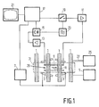
- the magnetic resonance apparatus which is diagrammatically shown in Fig. 1 comprises a first magnet system 1 for generating a steady magnetic field H, a second magnet system 3 for generating magnetic gradient fields, and first and second power supply sources 5 and 7 for the first magnet system 1 and the second magnet system 3, respectively.
- An RF coil 9 serves to generate an RF magnetic alternating field; to this end, it is connected to an RF source 11.
- the RF coil 9 For detection of nuclear spin resonance signals generated by the RF transmitted field in an object to be examined (not shown), use can also be made of the RF coil 9; to this end, this coil is connected to a receiving device 13 for RF signals.
- the output of the receiving device 13 is connected to a detector circuit 15 which is connected to a central control device 17.
- the central control device 17 also controls a modulator 19 for the RF source 11, the second power supply source 7, and a monitor 21 for image display.
- An RF oscillator 23 controls the modulator 19 as well as the detector 15 processing the measurement signals.
- a cooling device 25 comprising cooling ducts 27.
- a cooling device of this kind may be constructed as a water-cooling system for resistive coils or, as for the high field strengths required in the present case, for example, as a liquid-helium cooling system for superconducting magnet coils.
- a steady magnetic field H gradient fields for selecting object slices
- a spatially uniform RF alternating field can be generated in the measurement space 29 .
- the RF coil 9 can combine the functions of transmitter coil and measuring coil. Alternatively, different coils can be used for the two functions; for example, the measuring coils can be constructed as surface coils or butterfly coils, see US-A-4 816 765 (PHN 11.934) or as bird cage coils, see US-A-4 737 718 (PHN 11.466).
- the RF coil 9 will be referred to only as a measuring coil. If desired, the coil 9 may be enclosed by a Faraday cage 31 shielding RF fields.
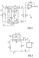
- Fig. 2 shows a circuit diagram of the RF coil 9 and a part of the receiving device 13.
- the RF coil 9 comprises a circuit, tuned to a predetermined frequency, with a pure self-inductance 33, a tuning capacitor 35 and a loss resistor 37. Via two series-connected coupling capacitors 39 and 41, the RF coil 9 is connected to an input amplifier circuit 43 of the receiving device 13.
- the input amplifier circuit 43 comprises an operational amplifier 45 which is set by means of (very high-ohmic) resistors 47, 49 and 51.
- the input amplifier circuit 43 may also comprise other elements which are known per se , for example a network of coils and capacitors. It comprises first and second input terminals 53 and 55 and an output terminal 57.
- the first input terminal 53 is connected, via the two coupling capacitors 39 and 41, to a first end of the RF coil 9, and the second input terminal 55 is connected to the other end of the RF coil and to a reference point 59 of fixed potential.
- the output terminal 57 is connected to further parts of the receiving device 13 or directly to the detector 15.
- the load network 61 comprises a first series connection of a first switch 63 and a first resistor 65, and also a second series connection of a second switch 67 and a second resistor 69.
- the first and the second switches 63 and 67 are formed by first and second diodes, preferably PIN diodes.
- the anode of the first diode 63 and the cathode of the second diode 67 are connected ( via the coupling capacitor 41) to the first input terminal 53, the other electrodes of these diodes being connected to one end of the first resistor 65 and the second resistor 69, respectively.
- the other end of the first resistor 65 is connected to a control terminal 71 and to an electrode of a capacitor 73, the other electrode of which is connected to the reference point 59.
- the other end of the second resistor 69 is connected directly to the reference point 59.
- a positive or negative direct voltage, relative to the reference point 59, can be applied, as desired, to the control terminal 71 via switching means (not shown).
- control voltage the applied direct voltage
- both diodes 63, 65 are blocked so that the load network 61 has no effect on the quality Q of the RF coil 9.
- This is the state which occurs when the apparatus is used for a normal measurement.
- a negative control voltage of, for example -10 V is applied, so that both diodes 63, 67 become conductive.
- the diodes thus act as switches which, in the conductive state, connect one end of the first and the second resistors 65, 69, to the first input terminal 53 and hence also to the RF coil 9.
- the other end of the first resistor 65 is connected, via the capacitor 73, to the second input terminal 55 whereas the other end of the second resistor 69 is connected directly to the second input terminal, so that for RF signals these two resistors are connected in parallel and interconnect the two input terminals. They thus constitute a load resistance for the RF coil 9 which simulates a coil load caused by a patient.
- the first resistor 65, the two diodes 63, 67 and the second resistor 69 are connected in series between the control terminal 71 and the reference point 59.
- a resistor 75, 77 is connected parallel to each of these diodes. The values of these resistors are preferably equal and very high.
- a frequency shift caused by the presence of the patient can also be simulated by connecting an impedance 79 parallel to the second resistor 69.
- the impedance 79 simply consists of a capacitor, so that the impedance is of a capacitive nature.
- a shift to a lower frequency is thus simulated, which shift has been found to occur most frequently in practice.
- a frequency shift to higher values could be simulated by an impedance 79 of an inductive nature, for example by replacing the capacitor by a coil.
- the switches 63 and 67 may also be formed by other, known switching elements, for example transistors, instead of PIN diodes. If desired, the first and second resistors 65, 69 and the impedance 79 may be constructed so as to be variable.
- the load circuit 69 can be combined with the RF coil 9 so as to form one structural unit.
- control voltage can be applied via a high self-inductance or via an RF rejection filter, comprising a parallel connection of a self-inductance and a capacitor. In that case complete isolation for RF signals exists between the control voltage source and the load network 61.
- Fig. 3 shows an embodiment in which the load network 61' comprises a parallel connection of a switch 63' and a resistor 65'.
- This parallel connection is included in the circuit forming the RF coil 9.
- the switch 61' can be opened or closed by applying a suitable control voltage to the control terminal 71'.
- the resistor 65' is connected in series with the loss resistor 37 and, when the switch is closed, the resistor is short-circuited.
- the resistor 65' can be coupled to the RF coil 9 by means of the switch 63'.
- the switch 63' and the resistor 65' analogous to the description given with reference to Fig. 2.
Landscapes
- Physics & Mathematics (AREA)
- Condensed Matter Physics & Semiconductors (AREA)
- General Physics & Mathematics (AREA)
- High Energy & Nuclear Physics (AREA)
- Magnetic Resonance Imaging Apparatus (AREA)
Priority Applications (1)
| Application Number | Priority Date | Filing Date | Title |
|---|---|---|---|
| EP19930202716 EP0590712B1 (fr) | 1992-09-29 | 1993-09-20 | Appareil à résonance magnétique |
Applications Claiming Priority (3)
| Application Number | Priority Date | Filing Date | Title |
|---|---|---|---|
| EP92202975 | 1992-09-29 | ||
| EP92202975 | 1992-09-29 | ||
| EP19930202716 EP0590712B1 (fr) | 1992-09-29 | 1993-09-20 | Appareil à résonance magnétique |
Publications (2)
| Publication Number | Publication Date |
|---|---|
| EP0590712A1 true EP0590712A1 (fr) | 1994-04-06 |
| EP0590712B1 EP0590712B1 (fr) | 1997-08-20 |
Family
ID=26131715
Family Applications (1)
| Application Number | Title | Priority Date | Filing Date |
|---|---|---|---|
| EP19930202716 Expired - Lifetime EP0590712B1 (fr) | 1992-09-29 | 1993-09-20 | Appareil à résonance magnétique |
Country Status (1)
| Country | Link |
|---|---|
| EP (1) | EP0590712B1 (fr) |
Cited By (4)
| Publication number | Priority date | Publication date | Assignee | Title |
|---|---|---|---|---|
| GB2288024A (en) * | 1994-03-30 | 1995-10-04 | Oxford Instr | Diode-type NMR RF transmitter decoupling circuit |
| WO2009153705A1 (fr) | 2008-06-20 | 2009-12-23 | Koninklijke Philips Electronics N.V. | Dispositif simulateur de charge électronique pour tester des enroulements hf |
| WO2010146487A1 (fr) * | 2009-06-19 | 2010-12-23 | Koninklijke Philips Electronics, N.V. | Utilisation de dispositifs memristance pour bobines rf d'irm |
| CN109477874A (zh) * | 2016-06-28 | 2019-03-15 | 皇家飞利浦有限公司 | 具有改善的热性能的磁共振成像 |
Citations (4)
| Publication number | Priority date | Publication date | Assignee | Title |
|---|---|---|---|---|
| US4717881A (en) * | 1985-11-15 | 1988-01-05 | Technicare Corporation | Radio frequency coils for nuclear magnetic resonance imaging systems |
| US4719406A (en) * | 1986-02-07 | 1988-01-12 | General Electric Company | Phantom for performance evaluation of a nuclear magnetic resonance scanner |
| US4731585A (en) * | 1987-02-24 | 1988-03-15 | Kabushiki Kaisha Toshiba | Antenna coupling circuit for magnetic resonance imaging |
| US5051700A (en) * | 1990-03-19 | 1991-09-24 | Kabushiki Kaisha Toshiba | Feedback circuit for noiseless damping of the Q of an MRI receiver coil antenna |
-
1993
- 1993-09-20 EP EP19930202716 patent/EP0590712B1/fr not_active Expired - Lifetime
Patent Citations (4)
| Publication number | Priority date | Publication date | Assignee | Title |
|---|---|---|---|---|
| US4717881A (en) * | 1985-11-15 | 1988-01-05 | Technicare Corporation | Radio frequency coils for nuclear magnetic resonance imaging systems |
| US4719406A (en) * | 1986-02-07 | 1988-01-12 | General Electric Company | Phantom for performance evaluation of a nuclear magnetic resonance scanner |
| US4731585A (en) * | 1987-02-24 | 1988-03-15 | Kabushiki Kaisha Toshiba | Antenna coupling circuit for magnetic resonance imaging |
| US5051700A (en) * | 1990-03-19 | 1991-09-24 | Kabushiki Kaisha Toshiba | Feedback circuit for noiseless damping of the Q of an MRI receiver coil antenna |
Non-Patent Citations (3)
| Title |
|---|
| S.J. JENNINGS ET AL.: "SIMULATION OF PATIENT LOADING IN NUCLEAR MAGNETIC RESONANCE IMAGING THROUGH THE USE OF INDUCTIVE DAMPING LOOPS", THE BRITISH JOURNAL OF RADIOLOGY, vol. 59, no. 706, 1 October 1986 (1986-10-01), LONDON, GB, pages 1031 - 1034 * |
| T.J. LAWRY ET AL.: "COMPUTER MODELING OF SURFACE COIL SENSITIVITY", MAGNETIC RESONANCE IN MEDICINE., vol. 16, no. 2, 1 November 1990 (1990-11-01), DULUTH,MN US, pages 294 - 302, XP000175910 * |
| W.A. EDELSTEIN ET AL.: "A SIGNAL-TO-NOISE CALIBRATION PROCEDURE FOR NMR IMAGING SYSTEMS", MEDICAL PHYSICS., vol. 11, no. 2, 1 March 1984 (1984-03-01), NEW YORK US, pages 180 - 185, XP002324567, DOI: doi:10.1118/1.595484 * |
Cited By (10)
| Publication number | Priority date | Publication date | Assignee | Title |
|---|---|---|---|---|
| GB2288024A (en) * | 1994-03-30 | 1995-10-04 | Oxford Instr | Diode-type NMR RF transmitter decoupling circuit |
| GB2288024B (en) * | 1994-03-30 | 1998-03-18 | Oxford Instr | Oscillating magnetic field generating assembly |
| WO2009153705A1 (fr) | 2008-06-20 | 2009-12-23 | Koninklijke Philips Electronics N.V. | Dispositif simulateur de charge électronique pour tester des enroulements hf |
| US8633706B2 (en) | 2008-06-20 | 2014-01-21 | Koninklijke Philips N.V. | Electronic load simulator device for testing RF coils |
| WO2010146487A1 (fr) * | 2009-06-19 | 2010-12-23 | Koninklijke Philips Electronics, N.V. | Utilisation de dispositifs memristance pour bobines rf d'irm |
| CN102803981A (zh) * | 2009-06-19 | 2012-11-28 | 皇家飞利浦电子股份有限公司 | 将忆阻器装置用于mri rf 线圈 |
| US9417299B2 (en) | 2009-06-19 | 2016-08-16 | Koninklijke Philips N.V. | Using memristor devices as switches for MRI RF coils |
| CN102803981B (zh) * | 2009-06-19 | 2016-09-21 | 皇家飞利浦电子股份有限公司 | 将忆阻器装置用于mri rf 线圈 |
| CN109477874A (zh) * | 2016-06-28 | 2019-03-15 | 皇家飞利浦有限公司 | 具有改善的热性能的磁共振成像 |
| CN109477874B (zh) * | 2016-06-28 | 2021-10-29 | 皇家飞利浦有限公司 | 具有改善的热性能的磁共振成像 |
Also Published As
| Publication number | Publication date |
|---|---|
| EP0590712B1 (fr) | 1997-08-20 |
Similar Documents
| Publication | Publication Date | Title |
|---|---|---|
| RU2539794C2 (ru) | Использование мемисторных устройств для радиочастотных катушек при магнитно-резонансной томографии | |
| US4638252A (en) | Circuit for detecting RF coil assembly position in an MR scanner | |
| US20100277175A1 (en) | Tunable and/or detunable mr receive coil arrangements | |
| EP0529730B1 (fr) | Appareil à résonance magnétique muni de bobines réceptrices decouplées | |
| JPS61124854A (ja) | アンテナ装置 | |
| US4712069A (en) | Magnetic resonance imaging apparatus including two orthogonal r.f. coils | |
| NL8401671A (nl) | Kernspinresonantie apparaat met oppervlaktespoel detectie. | |
| JPH01170447A (ja) | 磁気共振映像装置 | |
| US5243287A (en) | Dynamically detuned NMR field coil | |
| EP2291671B1 (fr) | Dispositif simulateur de charge électronique pour tester des bobines rf | |
| Darnell et al. | Integrated radio‐frequency/wireless coil design for simultaneous MR image acquisition and wireless communication | |
| EP0590712B1 (fr) | Appareil à résonance magnétique | |
| US5387868A (en) | Magnetic resonance apparatus | |
| JPH0578339B2 (fr) | ||
| US4776341A (en) | Nuclear magnetic resonance tomography apparatus with galvanic connections to the examination subject | |
| US4810968A (en) | Magnetic resonance imaging apparatus comprising a pin diode uncoupled detection coil | |
| US5432451A (en) | Magnetic resonance imaging reflectometer tuning unit | |
| US5202634A (en) | Double surface coil for a nuclear magnetic resonance apparatus | |
| US4644282A (en) | Apparatus for the formation of images of an examination subject with nuclear magnetic resonance | |
| US20070038068A1 (en) | Mr imaging method | |
| JPH05277087A (ja) | 室温のシムコイルとの勾配コイル相互作用を減じるための方法及び装置 | |
| EP0361574A1 (fr) | Procédé et dispositif pour la compensation de courants de foucault dans des appareils à résonance magnétique | |
| WO2023178242A2 (fr) | Procédés et appareil d'irm mobile utilisant un aimant permanent | |
| US20250199097A1 (en) | Tunable radio frequency coil assembly and magnetic resonance system comprising the rf coil assembly | |
| JPH03141928A (ja) | バードケージコイル |
Legal Events
| Date | Code | Title | Description |
|---|---|---|---|
| PUAI | Public reference made under article 153(3) epc to a published international application that has entered the european phase |
Free format text: ORIGINAL CODE: 0009012 |
|
| AK | Designated contracting states |
Kind code of ref document: A1 Designated state(s): DE FR GB |
|
| RAP1 | Party data changed (applicant data changed or rights of an application transferred) |
Owner name: N.V. PHILIPS' GLOEILAMPENFABRIEKEN |
|
| 17P | Request for examination filed |
Effective date: 19940908 |
|
| GRAG | Despatch of communication of intention to grant |
Free format text: ORIGINAL CODE: EPIDOS AGRA |
|
| 17Q | First examination report despatched |
Effective date: 19961016 |
|
| GRAH | Despatch of communication of intention to grant a patent |
Free format text: ORIGINAL CODE: EPIDOS IGRA |
|
| GRAH | Despatch of communication of intention to grant a patent |
Free format text: ORIGINAL CODE: EPIDOS IGRA |
|
| GRAA | (expected) grant |
Free format text: ORIGINAL CODE: 0009210 |
|
| AK | Designated contracting states |
Kind code of ref document: B1 Designated state(s): DE FR GB |
|
| REF | Corresponds to: |
Ref document number: 69313226 Country of ref document: DE Date of ref document: 19970925 |
|
| ET | Fr: translation filed | ||
| PLBE | No opposition filed within time limit |
Free format text: ORIGINAL CODE: 0009261 |
|
| 26N | No opposition filed | ||
| REG | Reference to a national code |
Ref country code: FR Ref legal event code: CD |
|
| REG | Reference to a national code |
Ref country code: GB Ref legal event code: IF02 |
|
| PGFP | Annual fee paid to national office [announced via postgrant information from national office to epo] |
Ref country code: FR Payment date: 20020926 Year of fee payment: 10 |
|
| PGFP | Annual fee paid to national office [announced via postgrant information from national office to epo] |
Ref country code: GB Payment date: 20020927 Year of fee payment: 10 |
|
| REG | Reference to a national code |
Ref country code: GB Ref legal event code: 746 Effective date: 20020906 |
|
| PGFP | Annual fee paid to national office [announced via postgrant information from national office to epo] |
Ref country code: DE Payment date: 20021119 Year of fee payment: 10 |
|
| REG | Reference to a national code |
Ref country code: FR Ref legal event code: D6 |
|
| PG25 | Lapsed in a contracting state [announced via postgrant information from national office to epo] |
Ref country code: GB Free format text: LAPSE BECAUSE OF NON-PAYMENT OF DUE FEES Effective date: 20030920 |
|
| PG25 | Lapsed in a contracting state [announced via postgrant information from national office to epo] |
Ref country code: DE Free format text: LAPSE BECAUSE OF NON-PAYMENT OF DUE FEES Effective date: 20040401 |
|
| GBPC | Gb: european patent ceased through non-payment of renewal fee |
Effective date: 20030920 |
|
| PG25 | Lapsed in a contracting state [announced via postgrant information from national office to epo] |
Ref country code: FR Free format text: LAPSE BECAUSE OF NON-PAYMENT OF DUE FEES Effective date: 20040528 |
|
| REG | Reference to a national code |
Ref country code: FR Ref legal event code: ST |