EP0590831A2 - Luminance and chrominance signal separation circuits - Google Patents
Luminance and chrominance signal separation circuits Download PDFInfo
- Publication number
- EP0590831A2 EP0590831A2 EP93307330A EP93307330A EP0590831A2 EP 0590831 A2 EP0590831 A2 EP 0590831A2 EP 93307330 A EP93307330 A EP 93307330A EP 93307330 A EP93307330 A EP 93307330A EP 0590831 A2 EP0590831 A2 EP 0590831A2
- Authority
- EP
- European Patent Office
- Prior art keywords
- signal
- circuit
- output
- filter means
- delay
- Prior art date
- Legal status (The legal status is an assumption and is not a legal conclusion. Google has not performed a legal analysis and makes no representation as to the accuracy of the status listed.)
- Granted
Links
Images


Classifications
-
- H—ELECTRICITY
- H04—ELECTRIC COMMUNICATION TECHNIQUE
- H04N—PICTORIAL COMMUNICATION, e.g. TELEVISION
- H04N9/00—Details of colour television systems
- H04N9/77—Circuits for processing the brightness signal and the chrominance signal relative to each other, e.g. adjusting the phase of the brightness signal relative to the colour signal, correcting differential gain or differential phase
- H04N9/78—Circuits for processing the brightness signal and the chrominance signal relative to each other, e.g. adjusting the phase of the brightness signal relative to the colour signal, correcting differential gain or differential phase for separating the brightness signal or the chrominance signal from the colour television signal, e.g. using comb filter
Definitions
- This invention relates to luminance and chrominance signal separation circuits.
- a luminance/chrominance (Y/C) separation circuit using a comb filter, for separating a composite video signal into a luminance signal and a chrominance signal is known, for example, from Japanese Patent Application No. 2-137081.
- FIG. 5 of the accompanying drawings shows a previously proposed Y/C separation circuit using a comb filter.
- a 1H (a period of one horizontal synchronization signal, or, briefly, one horizontal scanning period) delay line 4F outputs a composite video signal b obtained by delaying an input composite video signal a applied thereto by one horizontal scanning period, while a 1H delay line 4S outputs a composite video signal c obtained by delaying the composite video signal b output from the 1H delay line 4F by one horizontal scanning period.
- the input composite video signal a, the composite video signal b output from the 1H delay line 4F, and the composite video signal c output from the 1H delay line 4S correspond to the composite video signals for first, second, and third horizontal lines.
- a bandpass filter (BPF) 6 extracts a signal d as a high-frequency component of the input composite video signal a.
- a bandpass filter 8 extracts a signal e as a high-frequency component of the composite video signal b output from the 1H delay line 4F.
- a bandpass filter 10 extracts a signal f as a high-frequency component of the composite video signal c output from the 1H delay line 4S.
- a subtractor 122 subtracts the output signal d of the BPF 6 from the output signal e of the BPF 8, and a 1/2 (multiply by a half) circuit 124 outputs a signal g obtained by halving the output of the subtractor 122.
- a subtractor 142 subtracts the output signal f of the BPF 10 from the output signal e of the BPF 8, and a 1/2 circuit 144 outputs a signal h obtained by halving the output of the subtractor 142.
- An adder 162 adds up the signal g and the signal h, and a 1/2 circuit 164 outputs a signal obtained by halving the output signal of the adder 162, i.e., a chrominance signal i.
- a subtractor 170 subtracts the chrominance signal i from the composite video signal b output from the 1H delay line 4F and outputs the difference as a luminance signal j.
- a luminance and chrominance signal separation circuit for video signal processing apparatus, the circuit comprising: first delay means for delaying a composite video signal; second delay means connected to the first delay means serially; first filter means connected to an input terminal of the first delay means; second filter means connected to an input terminal of the second delay means; third filter means connected to an output terminal of said second delay means; and a level detection unit connected to output terminals of the first, second, and third filter means.
- a luminance and chrominance signal separation circuit for video signal processing apparatus, the circuit comprising: first delay means supplied with a composite video signal; second delay means connected to the first delay means serially; first filter means connected to an input terminal of the first delay means; second filter means connected to an input terminal of the second delay means; third filter means connected to an output terminal of the second delay means; first comb filter means connected to an output terminal of the first filter means and an output terminal of the second filter means; second comb filter means connected to the output terminal of the second filter means and an output terminal of the third filter means; third comb filter means connected to an output terminal of the first comb filter means and an output terminal of the second comb filter means; and a switching circuit connected to the output terminal of the first comb filter means, the output terminal of the second comb filter means, and an output terminal of the third comb filter means.
- An embodiment of the invention described below provides a Y/C separation circuit capable of decreasing both the noise level and the noise frequency without deteriorating the high-frequency component of the luminance signal.
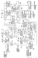
- FIG. 1 shows a structure of an embodiment of a Y/C separation circuit of the present invention.
- An input composite video signal is converted into a digital signal by an A/D converter 2.
- a delay line unit 4 is formed of a 1H delay line 4F and a 1H delay line 4S.
- the 1H delay line 4F outputs a composite video signal obtained by delaying the digitized composite video signal by one horizontal scanning period
- the 1H delay line 4S outputs a composite video signal obtained by delaying the composite video signal output from the 1H delay line 4F by one horizontal scanning period.
- the input composite video signal, the composite video signal output from the 1H delay line 4f, and the composite video signal output from the 1H delay line 4S correspond to the composite video signal for the first, second, and third horizontal lines.
- a BPF 6 extracts a signal of chrominance frequency band, i.e., a signal of high-frequency component, from the input composite video signal.
- a BPF 8 extracts a signal of chrominance frequency band, i.e., a signal of high-frequency component, from the composite video signal output from the 1H delay line 4F.
- a BPF 10 extracts a signal of chrominance frequency band, i.e., a signal of high-frequency component, from the composite video signal output from the 1H delay line 4S.
- the comb filter means of the embodiment shown in FIG. 1 is formed of 2-line comb filters 12 and 14 and a 3-line comb filter 16.
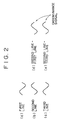
- the 2-line comb filter 12 receiving the output signal of the BPF 6 and the output signal of the BPF 8, subtracts the output signal of the BPF 6, i.e., the composite video signal for the first horizontal line (refer to FIG. 2(a)), from the output signal of the BPF 8, i.e., the composite video signal for the second horizontal line (refer to FIG. 2(b)), and outputs a chrominance signal (refer to FIG. 2(d)).
- the 2-line comb filter 14 receiving the output signal of the BPF 8 and the output signal of the BPF 10, subtracts the output signal of the BPF 10, i.e., the composite video signal for the third horizontal line (refer to FIG. 2(c)), from the output signal of the BPF 8, i.e., the composite video signal for the second horizontal line (refer to FIG. 2(b)), and outputs a chrominance signal (refer to FIG. 2(e)). Since the phase of the composite signal is inverted every line as shown in FIGs. 2(a), (b), and (c), the chrominance signal is obtained by the above described subtraction.
- the 3-line comb filter 16 adds up the output signals of the 2-line comb filters 12 and 14 and outputs a chrominance signal. By the addition, signal components other than the chrominance signal are eliminated.
- a BPF processing circuit 18 extracts a signal of a predetermined frequency band from the output signal of the BPF 8 to thereby output a chrominance signal.
- the frequency band for the BPF processing circuit 18 is selected to be an appropriate band not producing errors due to a sweep signal and the like. As described above, there are generated four types of chrominance signals in the embodiment of FIG. 1.
- a level detection unit LD detects the level of a high-frequency component of the luminance signal included in the composite video signal.
- the level detection unit LD is formed of a first level detecting portion for detecting the level of the high-frequency component of the luminance signal in the composite video signal for the first and second horizontal lines and a second level detecting portion for detecting the level of the high-frequency component of the luminance signal in the composite video signal for the second and third horizontal lines.
- the first level detecting portion includes an adder 22 for adding up the output signal of the BPF 6, i.e., the signal for the first line of the composite video signal (refer to FIG. 3(a) or (c)), and the output signal of the BPF 8, i.e., the signal for the second line of the composite video signal (refer to FIG. 3(b) or (d)), an absolute circuit 24 for obtaining an absolute value of the output of the adder 22 (refer to FIG. 3(e) (when the high-frequency component is present in the luminance signal) or refer to FIG. 3(f) (when the high-frequency component is absent in the luminance signal)), and an LPF 26 for applying a low-pass filtering (LPF) treatment to the output signal of the absolute circuit 24.
- LPF low-pass filtering
- the second level detecting portion includes an adder 28 for adding up the output signal of the BPF 8, i.e., the signal for the second line of the composite video signal, and the output signal of the BPF 10, i.e., the signal for the third line of the composite video signal, an absolute circuit 30 for obtaining an absolute value of the output of the adder 28, and an LPF 32 for applying a low-pass filtering (LPF) treatment to the output signal of the absolute circuit 30.
- LPF low-pass filtering
- a comparing circuit 34 receiving the output signals of the LPFs 26 and 32, i.e., the level of the high-frequency signal component of the luminance signal in the composite video signal for the first and second lines and the level of the high-frequency signal component of the luminance signal in the composite video signal for the second and third lines, outputs a select signal M of the 2-line comb filter 12 (refer to M in FIG. 4), a select signal N of the 2-line comb filter 14 (refer to N in FIG. 4), a select signal O of the 3-line comb filter 16 (refer to O in FIG. 4), or a select signal P of the BPF processing circuit 18 (refer to P in FIG. 4).
- a comparing unit CC shown in FIG. 1 and FIG. 4, includes comparing circuits 36 and 38 and a switch circuit 40 (denoted by reference numeral 52 in FIG. 4).
- the comparing circuit 36 decides whether or not the level of the high-frequency signal component of the luminance signal in the composite video signal for the first and second horizontal lines is lower than a predetermined comparison level.
- the comparing circuit 38 decides whether or not the level of the high-frequency signal component of the luminance signal in the composite video signal for the second and third horizontal lines is lower than a predetermined comparison level.
- a switch circuit 40 receiving the results of comparison from the comparing circuits 36 and 38, when the level of the high-frequency signal component of the luminance signal for the first and second horizontal lines is lower than the predetermined level and when the level of the high-frequency signal component of the luminance signal for the second and third horizontal lines is lower than the predetermined level, outputs an instruction to select the chrominance signal output from the BPF processing circuit 18 (i.e., an instruction to select the trap filter).
- the switch circuit 40 When at least one of the level of the high-frequency signal component of the luminance signal for the first and second horizontal lines and the level of the high-frequency signal component of the luminance signal for the second and third horizontal lines is higher than the predetermined level, the switch circuit 40 outputs an enable signal to allow the select signal output from the comparing circuit 34 as it is to be accepted.
- a switching control circuit 44 which is denoted in FIG. 4 by reference numerals 62, 64, 66, 68, 72, 74, 76, and 78, is supplied with outputs of the comparing circuit 34 and the switch circuit 40.
- the switching control circuit 44 When the switch circuit 40 has output an instruction to select the chrominance signal output from the BPF processing circuit 18, the switching control circuit 44 outputs an instruction signal to a switching circuit 20 such that the BPF processing circuit 18 is selected.
- the switch circuit 40 has output the enable signal, the content of the 2-line comb filter 12 select signal M, the 2-line comb filter 14 select signal N, the 3-line comb filter 16 select signal O, or the BPF processing circuit 18 select signal P as it is is output to the switching circuit 20.
- FIG. 4 shows an example of structure of the comparing circuits 36 and 38, the switch circuit 40, and the switching control circuit 44 in the embodiment of FIG. 1.
- the switch circuit 40 is formed of a NAND gate 52 and an inverter 54
- the switching control circuit 44 is formed of NAND gates 62, 64, and 66, a NOR gate 68, and D flip-flops 72, 74, 76, and 78.
- the comparing circuit 36 determines whether or not an 8-bit input A indicating the level of the high-frequency signal component of the luminance signal in the composite video signal for the first and second lines is lower than an 8-bit input B indicating a predetermined comparison level.
- the output of the comparing circuit 36 is input to a second input of the NAND gate 52.
- the comparing circuit 38 determines whether or not an 8-bit input A indicating the level of the high-frequency signal component of the luminance signal in the composite video signal for the second and third lines is lower than an 8-bit input B indicating a predetermined comparison level.
- the output of the comparing circuit 38 is input to a third input of the NAND gate 52.
- the first input of the NAND gate 52 is supplied with an "H" level.
- the inputs on one side of the NAND gates 62, 64, and 66 and the NOR gate 68 are supplied with the select signal M of the 2-line comb filter 12, the select signal N of the 2-line comb filter 14, the select signal O of the 3-line comb filter 16, and the select signal P of the BPF processing circuit 18, respectively.
- the inputs on the other side of the NAND gates 62, 64, and 66 is supplied with an output X of the NAND gate 52.
- the input on the other side of the NOR gate 68 is supplied with an output Y of the inverter 54 obtained by inverting the output of the NAND gate 52.
- the outputs of the NAND gates 62, 64, and 66 and the NOR gate 68 are supplied to the D inputs of the D flip-flops 72, 74, 76, and 78, respectively.
- the Q output of any of the D flip-flops 72, 74, 76, and 78 is "L", it indicates that the corresponding 2-line comb filter 12, 2-line comb filter 14, 3-line comb filter 16, or the BPF processing circuit 18 should be selected.
- the comparing circuit 36 When the level of the high-frequency signal component of the luminance signal for the first and second lines is lower than a predetermined comparison level, for example "5", the comparing circuit 36 outputs an "H” output. When the level of the high-frequency signal component of the luminance signal for the second and third lines is lower than a predetermined comparison level, for example "5", the comparing circuit 38 outputs an "H” output. The fact that the outputs of the comparing circuits 36 and 38 are both "H" indicates that luminance signal for successive lines are flat and have no level difference therebetween.
- the outputs of the comparing circuits 36 and 38 becomes “L". Accordingly, the output X of the NAND gate 52 becomes "H” and the output Y of the inverter 54 becomes “L”. As a result, the outputs of the NAND gates 62, 64, and 66 and the NOR gate 68 come to reflect the select signal M of the 2-line comb filter 12, the select signal N of the 2-line comb filter 14, the select signal O of the 3-line comb filter 16, and the select signal P of the BPF processing circuit 18, as it is, respectively.
- the NAND gates 62, 64, and 66 and the NOR gate 68 when receiving the select signal M ("H") of the 2-line comb filter 12, the select signal N ("H") of the 2-line comb filter 14, the select signal O ("H") of the 3-line comb filter 16, and the select signal P ("H") of the BPF processing circuit 18, respectively, provide an "L” output. Accordingly, the D flip-flop 72, 74, 76, or 78 whose D input is "L” provides an "L” output.
- the switching circuit 20 selectively outputs one of the chrominance signals output from the 2-line comb filter 12, 2-line comb filter 14, 3-line comb filter 16, and the BPF processing circuit 18 corresponding to the output of the switching control circuit 44.
- a D/A converter 46 converts the chrominance signal selected by the switching circuit 20 into an analog signal and outputs this signal.
- a luminance signal processing circuit 48 subtracts the chrominance signal selected by the switching circuit 20 from the composite video signal output. from the 1-H delay line 4F and outputs the thus obtained luminance signal.
- a D/A converter 50 converts the luminance signal output from the luminance signal processing circuit 48 into an analog signal and outputs this signal.
- the chrominance signal from the BPF processing circuit 18 is selected (i.e., the trap filter is switch selected).
- the high-frequency component of the luminance signal is zero, the luminance signal is flat and has no difference between lines, and therefore, even if the chrominance signal from the BPF processing circuit 18 is selected (if the trap filter is switch selected) there is produced no deterioration in the high-frequency component of the luminance signal.
- the level of the noise is low, and therefor, by setting the comparison level in the comparing circuits 36 and 38 to an appropriate value, it is achieved to cause the chrominance signal from the BPF processing circuit 18 to be selected (the trap filter to be switch selected) only for the pixel in which the noise is present, so that the noise level is lowered by the filter, the noise is prevented from vertically expanding on the picture screen (i.e., it is prevented from spreading over other horizontal lines), and the noise frequency is reduced to 1/3.
- a comb filter is selected so that a signal deterioration is prevented from occurring.
- the NTSC carrier signal which can leak out when an NTSC signal is converted to a PAL signal in a broadcasting station, produces a low-level vertical line on the picture screen.
- Such a signal can be eliminated by setting the comparison level in the comparing circuits 36 and 38 to an appropriate value so that the chrominance signal from the BPF processing circuit 18 is selected (the trap filter is switch selected). Since such a leakage signal is contained in the same component as the luminance signal, it has been unremovable by a conventional comb filter. However, since it is of a low level, it can be removed by the above embodiment.
- the embodiment is also applicable to the PAL signal by replacing the 1-H delay lines 4F and 4S with 2-H delay lines.
- the Y/C separation circuit embodying the invention is operative such that a chrominance signal as the output of bandpass filter means is selected and output when the level of the high-frequency component of a luminance signal is lower than a predetermined level, the noise frequency can be reduced as compared with that in the Y/C separation circuit of FIG. 5 while the high-frequency component of the luminance signal is not deteriorated and the noise level is equally lowered. More specifically, when the level of the high-frequency component of the luminance signal is low, the high-frequency component is not deteriorated even if the chrominance signal is generated by means of a bandpass filter (i.e., even if a trap filter is switch selected).
- a chrominance signal when a chrominance signal is generated by means of the bandpass filter, the noise is prevented from expanding in the vertical direction, i.e., from spreading over a plurality of horizontal lines, and hence the noise frequency is reduced.
- the level of the high-frequency component of the luminance signal is high, a chrominance signal is generated by comb filter means, and therefore, no signal deterioration is produced.
- the NTSC carrier signal leaking out when an NTSC signal is converted to a PAL signal in a broadcasting station which has been unremovable by the previously proposed Y/C separation circuit, can be removed by the Y/C separation circuit embodying the invention.
Landscapes
- Engineering & Computer Science (AREA)
- Multimedia (AREA)
- Signal Processing (AREA)
- Processing Of Color Television Signals (AREA)
Abstract
Description
- This invention relates to luminance and chrominance signal separation circuits.
- A luminance/chrominance (Y/C) separation circuit using a comb filter, for separating a composite video signal into a luminance signal and a chrominance signal, is known, for example, from Japanese Patent Application No. 2-137081.
- FIG. 5 of the accompanying drawings shows a previously proposed Y/C separation circuit using a comb filter. A 1H (a period of one horizontal synchronization signal, or, briefly, one horizontal scanning period)
delay line 4F outputs a composite video signal b obtained by delaying an input composite video signal a applied thereto by one horizontal scanning period, while a1H delay line 4S outputs a composite video signal c obtained by delaying the composite video signal b output from the1H delay line 4F by one horizontal scanning period. The input composite video signal a, the composite video signal b output from the1H delay line 4F, and the composite video signal c output from the1H delay line 4S correspond to the composite video signals for first, second, and third horizontal lines. - A bandpass filter (BPF) 6 extracts a signal d as a high-frequency component of the input composite video signal a. A
bandpass filter 8 extracts a signal e as a high-frequency component of the composite video signal b output from the1H delay line 4F. Abandpass filter 10 extracts a signal f as a high-frequency component of the composite video signal c output from the1H delay line 4S. - A
subtractor 122 subtracts the output signal d of theBPF 6 from the output signal e of theBPF 8, and a 1/2 (multiply by a half)circuit 124 outputs a signal g obtained by halving the output of thesubtractor 122. Asubtractor 142 subtracts the output signal f of theBPF 10 from the output signal e of theBPF 8, and a 1/2circuit 144 outputs a signal h obtained by halving the output of thesubtractor 142. Anadder 162 adds up the signal g and the signal h, and a 1/2circuit 164 outputs a signal obtained by halving the output signal of theadder 162, i.e., a chrominance signal i. Asubtractor 170 subtracts the chrominance signal i from the composite video signal b output from the1H delay line 4F and outputs the difference as a luminance signal j. - In the circuit shown in FIG. 5, while the level of a random noise in the luminance signal j is reduced to 1/2, if a granular random noise is contained in the composite video signal a, there are produced noises in the outputs e, d, and f of the
BPFs - When an NTSC signal is converted into a PAL signal in a broadcasting station, sometimes the carrier signal of the NTSC signal leaks out and becomes a low-level vertical line. Since this carrier signal is output from the j terminal the same as the luminance signal, it has been unable to be eliminated by the circuit shown in FIG. 5.
- When a trap filter is used instead of the above mentioned comb filter, an increase in noise can be prevented, but there arises a problem that the high-frequency component of the luminance signal becomes deteriorated.
- According to one aspect of the present invention there is provided a luminance and chrominance signal separation circuit for video signal processing apparatus, the circuit comprising:
first delay means for delaying a composite video signal;
second delay means connected to the first delay means serially;
first filter means connected to an input terminal of the first delay means;
second filter means connected to an input terminal of the second delay means;
third filter means connected to an output terminal of said second delay means; and
a level detection unit connected to output terminals of the first, second, and third filter means. - According to another aspect of the present invention there is provided a luminance and chrominance signal separation circuit for video signal processing apparatus, the circuit comprising:
first delay means supplied with a composite video signal;
second delay means connected to the first delay means serially;
first filter means connected to an input terminal of the first delay means;
second filter means connected to an input terminal of the second delay means;
third filter means connected to an output terminal of the second delay means;
first comb filter means connected to an output terminal of the first filter means and an output terminal of the second filter means;
second comb filter means connected to the output terminal of the second filter means and an output terminal of the third filter means;
third comb filter means connected to an output terminal of the first comb filter means and an output terminal of the second comb filter means; and
a switching circuit connected to the output terminal of the first comb filter means, the output terminal of the second comb filter means, and an output terminal of the third comb filter means. - An embodiment of the invention described below provides a Y/C separation circuit capable of decreasing both the noise level and the noise frequency without deteriorating the high-frequency component of the luminance signal.
- The invention will now be further described, by way of illustrative and non-limiting example, with reference to the accompanying drawings, in which:
- FIG. 1 is a block diagram of a Y/C separation circuit embodying the invention;
- FIG. 2 is a diagram showing chrominance signals;
- FIG. 3 is a diagram showing a high-frequency component of a luminance signal;
- FIG. 4 is a block diagram showing an example of comparing
circuits switch circuit 40, and aswitching control circuit 44 in the embodiment of FIG. 1; - FIG. 5 is a block diagram showing an example of a previously proposed Y/C separation circuit;
- FIG. 6 is a diagram showing signals at various portions of the circuit of FIG. 5 when a noise is produced in an output e of one
bandpass filter 8 due to a random noise contained in an input composite video signal a; - FIG. 7 is a diagram showing signals at various portions of the circuit of FIG. 5 when a noise is produced in an output d of another
bandpass filter 6 due to a random noise contained in the input composite video signal a; and - FIG. 8 is a diagram showing signals at various portions of the circuit of FIG. 5 when a noise is produced in an output f of another
bandpass filter 10 due to a random noise contained in the input composite video signal a. - FIG. 1 shows a structure of an embodiment of a Y/C separation circuit of the present invention. An input composite video signal is converted into a digital signal by an A/
D converter 2. A delay line unit 4 is formed of a1H delay line 4F and a1H delay line 4S. The1H delay line 4F outputs a composite video signal obtained by delaying the digitized composite video signal by one horizontal scanning period, while the1H delay line 4S outputs a composite video signal obtained by delaying the composite video signal output from the1H delay line 4F by one horizontal scanning period. The input composite video signal, the composite video signal output from the 1H delay line 4f, and the composite video signal output from the1H delay line 4S correspond to the composite video signal for the first, second, and third horizontal lines. - A
BPF 6 extracts a signal of chrominance frequency band, i.e., a signal of high-frequency component, from the input composite video signal. ABPF 8 extracts a signal of chrominance frequency band, i.e., a signal of high-frequency component, from the composite video signal output from the1H delay line 4F. ABPF 10 extracts a signal of chrominance frequency band, i.e., a signal of high-frequency component, from the composite video signal output from the1H delay line 4S. - The comb filter means of the embodiment shown in FIG. 1 is formed of 2-
line comb filters line comb filter 16. The 2-line comb filter 12, receiving the output signal of theBPF 6 and the output signal of theBPF 8, subtracts the output signal of theBPF 6, i.e., the composite video signal for the first horizontal line (refer to FIG. 2(a)), from the output signal of theBPF 8, i.e., the composite video signal for the second horizontal line (refer to FIG. 2(b)), and outputs a chrominance signal (refer to FIG. 2(d)). The 2-line comb filter 14, receiving the output signal of theBPF 8 and the output signal of theBPF 10, subtracts the output signal of theBPF 10, i.e., the composite video signal for the third horizontal line (refer to FIG. 2(c)), from the output signal of theBPF 8, i.e., the composite video signal for the second horizontal line (refer to FIG. 2(b)), and outputs a chrominance signal (refer to FIG. 2(e)). Since the phase of the composite signal is inverted every line as shown in FIGs. 2(a), (b), and (c), the chrominance signal is obtained by the above described subtraction. The 3-line comb filter 16 adds up the output signals of the 2-line comb filters BPF processing circuit 18 extracts a signal of a predetermined frequency band from the output signal of theBPF 8 to thereby output a chrominance signal. The frequency band for theBPF processing circuit 18 is selected to be an appropriate band not producing errors due to a sweep signal and the like. As described above, there are generated four types of chrominance signals in the embodiment of FIG. 1. - A level detection unit LD detects the level of a high-frequency component of the luminance signal included in the composite video signal. The level detection unit LD is formed of a first level detecting portion for detecting the level of the high-frequency component of the luminance signal in the composite video signal for the first and second horizontal lines and a second level detecting portion for detecting the level of the high-frequency component of the luminance signal in the composite video signal for the second and third horizontal lines.
- The first level detecting portion includes an
adder 22 for adding up the output signal of theBPF 6, i.e., the signal for the first line of the composite video signal (refer to FIG. 3(a) or (c)), and the output signal of theBPF 8, i.e., the signal for the second line of the composite video signal (refer to FIG. 3(b) or (d)), anabsolute circuit 24 for obtaining an absolute value of the output of the adder 22 (refer to FIG. 3(e) (when the high-frequency component is present in the luminance signal) or refer to FIG. 3(f) (when the high-frequency component is absent in the luminance signal)), and anLPF 26 for applying a low-pass filtering (LPF) treatment to the output signal of theabsolute circuit 24. - The second level detecting portion includes an
adder 28 for adding up the output signal of theBPF 8, i.e., the signal for the second line of the composite video signal, and the output signal of theBPF 10, i.e., the signal for the third line of the composite video signal, anabsolute circuit 30 for obtaining an absolute value of the output of theadder 28, and anLPF 32 for applying a low-pass filtering (LPF) treatment to the output signal of theabsolute circuit 30. - A comparing
circuit 34, receiving the output signals of theLPFs - A comparing unit CC, shown in FIG. 1 and FIG. 4, includes comparing
circuits reference numeral 52 in FIG. 4). The comparingcircuit 36 decides whether or not the level of the high-frequency signal component of the luminance signal in the composite video signal for the first and second horizontal lines is lower than a predetermined comparison level. The comparingcircuit 38 decides whether or not the level of the high-frequency signal component of the luminance signal in the composite video signal for the second and third horizontal lines is lower than a predetermined comparison level. - A
switch circuit 40, receiving the results of comparison from the comparingcircuits switch circuit 40 outputs an enable signal to allow the select signal output from the comparingcircuit 34 as it is to be accepted. - A switching
control circuit 44, which is denoted in FIG. 4 byreference numerals circuit 34 and theswitch circuit 40. When theswitch circuit 40 has output an instruction to select the chrominance signal output from theBPF processing circuit 18, the switchingcontrol circuit 44 outputs an instruction signal to aswitching circuit 20 such that theBPF processing circuit 18 is selected. When theswitch circuit 40 has output the enable signal, the content of the 2-line comb filter 12 select signal M, the 2-line comb filter 14 select signal N, the 3-line comb filter 16 select signal O, or theBPF processing circuit 18 select signal P as it is is output to the switchingcircuit 20. - FIG. 4 shows an example of structure of the comparing
circuits switch circuit 40, and the switchingcontrol circuit 44 in the embodiment of FIG. 1. In this example, theswitch circuit 40 is formed of aNAND gate 52 and aninverter 54, while the switchingcontrol circuit 44 is formed ofNAND gates gate 68, and D flip-flops - The comparing
circuit 36 determines whether or not an 8-bit input A indicating the level of the high-frequency signal component of the luminance signal in the composite video signal for the first and second lines is lower than an 8-bit input B indicating a predetermined comparison level. The output of the comparingcircuit 36 is input to a second input of theNAND gate 52. The comparingcircuit 38 determines whether or not an 8-bit input A indicating the level of the high-frequency signal component of the luminance signal in the composite video signal for the second and third lines is lower than an 8-bit input B indicating a predetermined comparison level. The output of the comparingcircuit 38 is input to a third input of theNAND gate 52. The first input of theNAND gate 52 is supplied with an "H" level. - The inputs on one side of the
NAND gates gate 68 are supplied with the select signal M of the 2-line comb filter 12, the select signal N of the 2-line comb filter 14, the select signal O of the 3-line comb filter 16, and the select signal P of theBPF processing circuit 18, respectively. The inputs on the other side of theNAND gates NAND gate 52. The input on the other side of the NORgate 68 is supplied with an output Y of theinverter 54 obtained by inverting the output of theNAND gate 52. - The outputs of the
NAND gates gate 68 are supplied to the D inputs of the D flip-flops flops line comb filter 12, 2-line comb filter 14, 3-line comb filter 16, or theBPF processing circuit 18 should be selected. - The operation of the circuits shown in FIG. 4 will be described below. When the level of the high-frequency signal component of the luminance signal for the first and second lines is lower than a predetermined comparison level, for example "5", the comparing
circuit 36 outputs an "H" output. When the level of the high-frequency signal component of the luminance signal for the second and third lines is lower than a predetermined comparison level, for example "5", the comparingcircuit 38 outputs an "H" output. The fact that the outputs of the comparingcircuits - When the outputs of the comparing
circuits NAND gate 52 becomes "L" and the output Y of theinverter 54 becomes "H". Accordingly, the outputs of theNAND gates gate 68 becomes "L". Hence, the outputs of the D flip-flops flop 78 becomes "L", and thereby theBPF processing circuit 18 is forcedly selected. - When at least one of the level of the high-frequency signal component of the luminance signal for the first and second lines and the level of the high-frequency signal component of the luminance signal for the second and third lines is higher than the predetermined comparison level, at least one of the outputs of the comparing
circuits NAND gate 52 becomes "H" and the output Y of theinverter 54 becomes "L". As a result, the outputs of theNAND gates gate 68 come to reflect the select signal M of the 2-line comb filter 12, the select signal N of the 2-line comb filter 14, the select signal O of the 3-line comb filter 16, and the select signal P of theBPF processing circuit 18, as it is, respectively. More specifically, theNAND gates gate 68, when receiving the select signal M ("H") of the 2-line comb filter 12, the select signal N ("H") of the 2-line comb filter 14, the select signal O ("H") of the 3-line comb filter 16, and the select signal P ("H") of theBPF processing circuit 18, respectively, provide an "L" output. Accordingly, the D flip-flop - Referring back to FIG. 1, the switching
circuit 20 selectively outputs one of the chrominance signals output from the 2-line comb filter 12, 2-line comb filter 14, 3-line comb filter 16, and theBPF processing circuit 18 corresponding to the output of the switchingcontrol circuit 44. - A D/
A converter 46 converts the chrominance signal selected by the switchingcircuit 20 into an analog signal and outputs this signal. A luminancesignal processing circuit 48 subtracts the chrominance signal selected by the switchingcircuit 20 from the composite video signal output. from the 1-H delay line 4F and outputs the thus obtained luminance signal. A D/A converter 50 converts the luminance signal output from the luminancesignal processing circuit 48 into an analog signal and outputs this signal. - As described above, when the level of the high-frequency component of the luminance signal is low in the embodiment shown in FIG. 1 to FIG. 4, the chrominance signal from the
BPF processing circuit 18 is selected (i.e., the trap filter is switch selected). When the high-frequency component of the luminance signal is zero, the luminance signal is flat and has no difference between lines, and therefore, even if the chrominance signal from theBPF processing circuit 18 is selected (if the trap filter is switch selected) there is produced no deterioration in the high-frequency component of the luminance signal. When a noise is input, the level of the noise is low, and therefor, by setting the comparison level in the comparingcircuits BPF processing circuit 18 to be selected (the trap filter to be switch selected) only for the pixel in which the noise is present, so that the noise level is lowered by the filter, the noise is prevented from vertically expanding on the picture screen (i.e., it is prevented from spreading over other horizontal lines), and the noise frequency is reduced to 1/3. When there is a high-frequency component of the luminance signal, a comb filter is selected so that a signal deterioration is prevented from occurring. Thus, by performing the above described switch selection, a dot crawl can be prevented from occurring at a noncorrelative portion located in the vertical direction. - The NTSC carrier signal, which can leak out when an NTSC signal is converted to a PAL signal in a broadcasting station, produces a low-level vertical line on the picture screen. Such a signal can be eliminated by setting the comparison level in the comparing
circuits BPF processing circuit 18 is selected (the trap filter is switch selected). Since such a leakage signal is contained in the same component as the luminance signal, it has been unremovable by a conventional comb filter. However, since it is of a low level, it can be removed by the above embodiment. - The embodiment is also applicable to the PAL signal by replacing the 1-
H delay lines - Since the Y/C separation circuit embodying the invention is operative such that a chrominance signal as the output of bandpass filter means is selected and output when the level of the high-frequency component of a luminance signal is lower than a predetermined level, the noise frequency can be reduced as compared with that in the Y/C separation circuit of FIG. 5 while the high-frequency component of the luminance signal is not deteriorated and the noise level is equally lowered. More specifically, when the level of the high-frequency component of the luminance signal is low, the high-frequency component is not deteriorated even if the chrominance signal is generated by means of a bandpass filter (i.e., even if a trap filter is switch selected). Further, when a chrominance signal is generated by means of the bandpass filter, the noise is prevented from expanding in the vertical direction, i.e., from spreading over a plurality of horizontal lines, and hence the noise frequency is reduced. When the level of the high-frequency component of the luminance signal is high, a chrominance signal is generated by comb filter means, and therefore, no signal deterioration is produced. Further, the NTSC carrier signal leaking out when an NTSC signal is converted to a PAL signal in a broadcasting station, which has been unremovable by the previously proposed Y/C separation circuit, can be removed by the Y/C separation circuit embodying the invention.
Claims (11)
- A luminance and chrominance signal separation circuit for video signal processing apparatus, the circuit comprising:
first delay means for delaying a composite video signal;
second delay means connected to said first delay means serially;
first filter means connected to an input terminal of said first delay means;
second filter means connected to an input terminal of said second delay means;
third filter means connected to an output terminal of said second delay means; and
a level detection unit connected to output terminals of said first, second, and third filter means. - A separation circuit as claimed in claim 1, comprising a comparing unit connected to output terminals of said level detection unit.
- A separation circuit as claimed in claim 2, wherein said comparing unit comprises:
a first comparing circuit for comparing the level of an output of said first low-pass filter with a comparison level signal;
a second comparing circuit for comparing the level of an output of said second low-pass filter with a comparison level signal;
a switch circuit for switching output signals of said first and second comparing circuits; and
a switching control circuit for switching output signals of said switch circuit and an output signal of said level detection unit. - A separation circuit as claimed in claim 3, wherein said switch circuit comprises a NAND gate.
- A separation circuit as claimed in claim 3 or claim 4, wherein said switching control circuit comprises plural logic gate circuits and plural flip-flop circuits.
- A separation circuit as claimed in any one of the preceding claims, wherein said level detection unit comprises:
first adder means for adding signals at its input terminals;
second adder means for adding signals at its input terminals;
a first absolute circuit for creating an absolute value of an output signal of said first adder means;
a second absolute circuit for creating an absolute value of an output signal of said second adder means;
first low-pass filter means connected to an output terminal of said first absolute circuit; and
second low-pass filter mean connected to an output terminal of said second absolute circuit. - A separation circuit as claimed in any one of the preceding claims, wherein the delay time of said first and second delay means nearly equals a period of one horizontal synchronization signal.
- A luminance and chrominance signal separation circuit for video signal processing apparatus, the circuit comprising:
first delay means supplied with a composite video signal;
second delay means connected to said first delay means serially;
first filter means connected to an input terminal of said first delay means;
second filter means connected to an input terminal of said second delay means;
third filter means connected to an output terminal of said second delay means;
first comb filter means connected to an output terminal of said first filter means and an output terminal of said second filter means;
second comb filter means connected to the output terminal of said second filter means and an output terminal of said third filter means;
third comb filter means connected to an output terminal of said first comb filter means and an output terminal of said second comb filter means; and
a switching circuit connected to the output terminal of said first comb filter means, the output terminal of said second comb filter means, and an output terminal of said third comb filter means. - A separation circuit as claimed in claim 8, comprising a luminance signal processing circuit for processing an output signal of said switching circuit and an output signal of said first delay means.
- A separation circuit as claimed in claim 9, comprising:
analog-to-digital converter means for converting the input signal to said first delay means;
first digital-to-analog converter means for converting an output signal of said luminance signal processing circuit; and
second digital-to-analog converter means for converting an output signal of said switching circuit. - A separation circuit as claimed in claim 8, claim 9 or claim 10, wherein the delay time of said first and second comb filter means nearly equals a period of two horizontal synchronization signals, and the delay time of said third comb filter means nearly equals a period of three horizontal synchronization signals.
Applications Claiming Priority (2)
| Application Number | Priority Date | Filing Date | Title |
|---|---|---|---|
| JP285177/92 | 1992-09-30 | ||
| JP28517792A JP3263791B2 (en) | 1992-09-30 | 1992-09-30 | YC separation circuit |
Publications (3)
| Publication Number | Publication Date |
|---|---|
| EP0590831A2 true EP0590831A2 (en) | 1994-04-06 |
| EP0590831A3 EP0590831A3 (en) | 1994-06-22 |
| EP0590831B1 EP0590831B1 (en) | 1999-03-17 |
Family
ID=17688101
Family Applications (1)
| Application Number | Title | Priority Date | Filing Date |
|---|---|---|---|
| EP93307330A Expired - Lifetime EP0590831B1 (en) | 1992-09-30 | 1993-09-16 | Luminance and chrominance signal separation circuits |
Country Status (4)
| Country | Link |
|---|---|
| US (1) | US5426470A (en) |
| EP (1) | EP0590831B1 (en) |
| JP (1) | JP3263791B2 (en) |
| DE (1) | DE69323947T2 (en) |
Cited By (5)
| Publication number | Priority date | Publication date | Assignee | Title |
|---|---|---|---|---|
| GB2288704A (en) * | 1994-04-21 | 1995-10-25 | Matsushita Electric Industrial Co Ltd | Chrominance and luminance separation |
| US5500687A (en) * | 1993-10-22 | 1996-03-19 | Matsushita Electric Industrial Co., Ltd. | Chrominance signal separator using chrominance signal correlation |
| EP0794677A3 (en) * | 1996-03-09 | 1997-09-24 | Deutsche Thomson-Brandt Gmbh | Method and circuit arrangement for separating luminance and chrominance signals from a composite colour signal |
| US5909255A (en) * | 1996-02-19 | 1999-06-01 | Matsushita Electric Industrial Co., Ltd. | Y/C separation apparatus |
| EP0845910A3 (en) * | 1996-11-01 | 1999-08-11 | Matsushita Electric Industrial Co., Ltd. | 2-Line YC separation device |
Families Citing this family (6)
| Publication number | Priority date | Publication date | Assignee | Title |
|---|---|---|---|---|
| EP0613311A1 (en) * | 1993-02-26 | 1994-08-31 | Kabushiki Kaisha Toshiba | Y/C separating circuit |
| JP3500883B2 (en) * | 1996-12-12 | 2004-02-23 | 松下電器産業株式会社 | Color system discrimination circuit |
| TWI280062B (en) * | 2005-10-13 | 2007-04-21 | Realtek Semiconductor Corp | Signal separation apparatus applied in image transmission system and related method |
| TWI347118B (en) * | 2006-02-14 | 2011-08-11 | Realtek Semiconductor Corp | Image processing device and method |
| TWI339527B (en) * | 2006-02-15 | 2011-03-21 | Realtek Semiconductor Corp | Method and apparatus for enhancing image quality |
| JP2008175845A (en) * | 2007-01-16 | 2008-07-31 | Fujitsu Ten Ltd | Display control device and display apparatus |
Family Cites Families (13)
| Publication number | Priority date | Publication date | Assignee | Title |
|---|---|---|---|---|
| NL8403487A (en) * | 1984-11-15 | 1986-06-02 | Stamicarbon | PROCESS FOR THE ENZYMATIC SEPARATION OF DL-ALFA-AMINOIC ACID AMIDS. |
| US4845547A (en) * | 1988-03-28 | 1989-07-04 | North American Philips Corporation | Non-linear comb filter for color TV receivers |
| JPH0271693A (en) * | 1988-09-06 | 1990-03-12 | Sony Corp | Luminance/chrominance separation circuit |
| DE3836043A1 (en) * | 1988-10-20 | 1990-04-26 | Thomson Brandt Gmbh | CIRCUIT FOR AN ADAPTIVE COMB FILTER FOR THE SEPARATION OF LUMINOUSITY SIGNAL AND COLOR TYPE SIGNAL OF AN FBAS-PAL SIGNAL |
| JPH0720265B2 (en) * | 1988-11-04 | 1995-03-06 | 三菱電機株式会社 | Video signal processing circuit |
| JPH0366287A (en) * | 1989-08-04 | 1991-03-20 | Matsushita Electric Ind Co Ltd | Signal separator |
| US5093715A (en) * | 1989-08-10 | 1992-03-03 | Sony Corporation | Adaptive comb filter for separating at least one component of a video signal |
| US5016092A (en) * | 1989-11-17 | 1991-05-14 | Rca Licensing Corporation | Control circuitry for an adaptive multistandard video comb filter |
| KR910013951A (en) * | 1989-12-12 | 1991-08-08 | 이헌조 | Luminance / Color Signal Separation Circuit of Composite Video Signal |
| KR0170630B1 (en) * | 1990-06-20 | 1999-03-20 | 강진구 | Luminance / Color Signal Preprocessor |
| KR930003177B1 (en) * | 1990-06-29 | 1993-04-23 | 삼성전자 주식회사 | Pattern-adaptive digital comb filter for separating luminance and color signals |
| KR930008184B1 (en) * | 1990-06-30 | 1993-08-26 | 삼성전자 주식회사 | Luminance / Color Signal Separation Circuit |
| DE4106076A1 (en) * | 1991-02-27 | 1992-09-03 | Philips Patentverwaltung | CIRCUIT ARRANGEMENT FOR SEPARATING A COLOR IMAGE SIGNAL INTO A COLOR SIGNAL AND A BRIGHTNESS SIGNAL |
-
1992
- 1992-09-30 JP JP28517792A patent/JP3263791B2/en not_active Expired - Fee Related
-
1993
- 1993-09-16 DE DE69323947T patent/DE69323947T2/en not_active Expired - Fee Related
- 1993-09-16 EP EP93307330A patent/EP0590831B1/en not_active Expired - Lifetime
- 1993-09-24 US US08/126,188 patent/US5426470A/en not_active Expired - Lifetime
Cited By (10)
| Publication number | Priority date | Publication date | Assignee | Title |
|---|---|---|---|---|
| US5500687A (en) * | 1993-10-22 | 1996-03-19 | Matsushita Electric Industrial Co., Ltd. | Chrominance signal separator using chrominance signal correlation |
| GB2288704A (en) * | 1994-04-21 | 1995-10-25 | Matsushita Electric Industrial Co Ltd | Chrominance and luminance separation |
| US5508753A (en) * | 1994-04-21 | 1996-04-16 | Matsushita Electric Industrial Co., Ltd. | Luminance and chrominance signal separating apparatus |
| GB2288704B (en) * | 1994-04-21 | 1998-07-22 | Matsushita Electric Industrial Co Ltd | Luminance and chrominance signal separating apparatus |
| US5909255A (en) * | 1996-02-19 | 1999-06-01 | Matsushita Electric Industrial Co., Ltd. | Y/C separation apparatus |
| CN1120634C (en) * | 1996-02-19 | 2003-09-03 | 松下电器产业株式会社 | Brightness signal and color signal separating device |
| EP0794677A3 (en) * | 1996-03-09 | 1997-09-24 | Deutsche Thomson-Brandt Gmbh | Method and circuit arrangement for separating luminance and chrominance signals from a composite colour signal |
| US5973753A (en) * | 1996-03-09 | 1999-10-26 | Deutsche Thomson-Brandt Gmbh | Method and circuit arrangement for separating luminance and chrominance signals of a CVBS signal |
| CN1112054C (en) * | 1996-03-09 | 2003-06-18 | 德国汤姆逊-布朗特公司 | The Method and circuits device that separates the composite video frequency band signal luminance and chrominance information |
| EP0845910A3 (en) * | 1996-11-01 | 1999-08-11 | Matsushita Electric Industrial Co., Ltd. | 2-Line YC separation device |
Also Published As
| Publication number | Publication date |
|---|---|
| EP0590831B1 (en) | 1999-03-17 |
| EP0590831A3 (en) | 1994-06-22 |
| JP3263791B2 (en) | 2002-03-11 |
| DE69323947D1 (en) | 1999-04-22 |
| DE69323947T2 (en) | 1999-09-16 |
| JPH06113324A (en) | 1994-04-22 |
| US5426470A (en) | 1995-06-20 |
Similar Documents
| Publication | Publication Date | Title |
|---|---|---|
| US5325186A (en) | Motion adaptive luminance signal and color signal separating filter | |
| US4924305A (en) | Motion detecting circuit for video signal processing using correlation techniques | |
| KR960006081B1 (en) | Motion detection circuit | |
| US5426470A (en) | Luminance and chrominance signal separation circuit employing comparison of level detected signal with a reference level | |
| JPH06125567A (en) | Brightness / color separation device | |
| KR100320901B1 (en) | Motion detection circuit | |
| KR930003178B1 (en) | Correlated Adaptive Luminance Signal and Color Signal Separation Circuit | |
| US5394193A (en) | Pattern-adaptive digital comb filter for separation of a luminance and a color signal | |
| KR0123768B1 (en) | Adaptive two-dimensional luminance / color signal separation method and apparatus | |
| JPH06311527A (en) | Adaptive picture peaking circuit using cross fader | |
| US5208662A (en) | Method of encoding color television signal and a circuit therefor | |
| KR0130951B1 (en) | Y/c separating circuit | |
| KR0126472B1 (en) | Adaptive Comb Filter for Chromaticity and Luminance Video Signal Separation and Signal Separation | |
| KR910007206B1 (en) | Adaptive luminance signal and color signal separator | |
| US4862252A (en) | Y/C separator circuit for separating luminance and chrominance signals conditioned on an ac luminance component | |
| US5373329A (en) | Method of picture movement signal detection and associated circuit | |
| JP3186336B2 (en) | Cross color reduction device in luminance signal color signal separation device | |
| KR100365848B1 (en) | Pure red color detection circuit and color compensation circuit using the same | |
| KR19980030424A (en) | Comb filter | |
| KR19980079061A (en) | A luminance and color signal separation method and a luminance and color signal separation circuit for performing the same | |
| US5523797A (en) | Luminance signal and color signal separating circuit | |
| JP2522433B2 (en) | Video motion signal detection circuit | |
| KR940005177B1 (en) | Lumina/chroma separation apparatus | |
| KR100248991B1 (en) | A luminance and color signal separation method and a luminance and color signal separation circuit for performing the same | |
| JP2626746B2 (en) | Color video signal processing circuit |
Legal Events
| Date | Code | Title | Description |
|---|---|---|---|
| PUAI | Public reference made under article 153(3) epc to a published international application that has entered the european phase |
Free format text: ORIGINAL CODE: 0009012 |
|
| AK | Designated contracting states |
Kind code of ref document: A2 Designated state(s): DE GB |
|
| PUAL | Search report despatched |
Free format text: ORIGINAL CODE: 0009013 |
|
| AK | Designated contracting states |
Kind code of ref document: A3 Designated state(s): DE GB |
|
| 17P | Request for examination filed |
Effective date: 19941122 |
|
| 17Q | First examination report despatched |
Effective date: 19970305 |
|
| GRAG | Despatch of communication of intention to grant |
Free format text: ORIGINAL CODE: EPIDOS AGRA |
|
| GRAG | Despatch of communication of intention to grant |
Free format text: ORIGINAL CODE: EPIDOS AGRA |
|
| GRAH | Despatch of communication of intention to grant a patent |
Free format text: ORIGINAL CODE: EPIDOS IGRA |
|
| GRAH | Despatch of communication of intention to grant a patent |
Free format text: ORIGINAL CODE: EPIDOS IGRA |
|
| GRAA | (expected) grant |
Free format text: ORIGINAL CODE: 0009210 |
|
| AK | Designated contracting states |
Kind code of ref document: B1 Designated state(s): DE GB |
|
| REF | Corresponds to: |
Ref document number: 69323947 Country of ref document: DE Date of ref document: 19990422 |
|
| PLBE | No opposition filed within time limit |
Free format text: ORIGINAL CODE: 0009261 |
|
| STAA | Information on the status of an ep patent application or granted ep patent |
Free format text: STATUS: NO OPPOSITION FILED WITHIN TIME LIMIT |
|
| 26N | No opposition filed | ||
| REG | Reference to a national code |
Ref country code: GB Ref legal event code: IF02 |
|
| PGFP | Annual fee paid to national office [announced via postgrant information from national office to epo] |
Ref country code: DE Payment date: 20070913 Year of fee payment: 15 |
|
| PGFP | Annual fee paid to national office [announced via postgrant information from national office to epo] |
Ref country code: GB Payment date: 20070912 Year of fee payment: 15 |
|
| GBPC | Gb: european patent ceased through non-payment of renewal fee |
Effective date: 20080916 |
|
| PG25 | Lapsed in a contracting state [announced via postgrant information from national office to epo] |
Ref country code: DE Free format text: LAPSE BECAUSE OF NON-PAYMENT OF DUE FEES Effective date: 20090401 |
|
| PG25 | Lapsed in a contracting state [announced via postgrant information from national office to epo] |
Ref country code: GB Free format text: LAPSE BECAUSE OF NON-PAYMENT OF DUE FEES Effective date: 20080916 |