EP0591900B1 - In Harz versiegeltes Halbleiterbauelement - Google Patents
In Harz versiegeltes Halbleiterbauelement Download PDFInfo
- Publication number
- EP0591900B1 EP0591900B1 EP93116022A EP93116022A EP0591900B1 EP 0591900 B1 EP0591900 B1 EP 0591900B1 EP 93116022 A EP93116022 A EP 93116022A EP 93116022 A EP93116022 A EP 93116022A EP 0591900 B1 EP0591900 B1 EP 0591900B1
- Authority
- EP
- European Patent Office
- Prior art keywords
- terminal
- casing
- connection portion
- wiring connection
- semiconductor device
- Prior art date
- Legal status (The legal status is an assumption and is not a legal conclusion. Google has not performed a legal analysis and makes no representation as to the accuracy of the status listed.)
- Expired - Lifetime
Links
Images


Classifications
-
- H—ELECTRICITY
- H10—SEMICONDUCTOR DEVICES; ELECTRIC SOLID-STATE DEVICES NOT OTHERWISE PROVIDED FOR
- H10W—GENERIC PACKAGES, INTERCONNECTIONS, CONNECTORS OR OTHER CONSTRUCTIONAL DETAILS OF DEVICES COVERED BY CLASS H10
- H10W70/00—Package substrates; Interposers; Redistribution layers [RDL]
- H10W70/40—Leadframes
- H10W70/481—Leadframes for devices being provided for in groups H10D8/00 - H10D48/00
-
- H—ELECTRICITY
- H10—SEMICONDUCTOR DEVICES; ELECTRIC SOLID-STATE DEVICES NOT OTHERWISE PROVIDED FOR
- H10W—GENERIC PACKAGES, INTERCONNECTIONS, CONNECTORS OR OTHER CONSTRUCTIONAL DETAILS OF DEVICES COVERED BY CLASS H10
- H10W76/00—Containers; Fillings or auxiliary members therefor; Seals
- H10W76/10—Containers or parts thereof
- H10W76/12—Containers or parts thereof characterised by their shape
-
- H—ELECTRICITY
- H10—SEMICONDUCTOR DEVICES; ELECTRIC SOLID-STATE DEVICES NOT OTHERWISE PROVIDED FOR
- H10W—GENERIC PACKAGES, INTERCONNECTIONS, CONNECTORS OR OTHER CONSTRUCTIONAL DETAILS OF DEVICES COVERED BY CLASS H10
- H10W76/00—Containers; Fillings or auxiliary members therefor; Seals
- H10W76/40—Fillings or auxiliary members in containers, e.g. centering rings
- H10W76/42—Fillings
- H10W76/47—Solid or gel fillings
Definitions
- the present invention relates to a resin-sealed semiconductor device, such as a diode, thyristor or transistor module, and, more particularly, to the structure of a terminal thereof used for connecting an external wiring to the device.
- Figs. 5(a) to (c) and 6 show a conventional resin-sealed semiconductor device and its terminal structure.
- numeral 1 represents a heat dissipating metal base
- 2 an insulating substrate
- 3 a semiconductor chip
- 4 a terminal
- 5 an outer casing made of resin
- 6 a sealing compound such as epoxy resin that fills the casing
- 7 a terminal nut mounted in a respective recess 5a on top of the outer casing 5.
- the figures actually show two terminals 4, two nuts 7, two recesses 5a etc. the number depending on the kind of semiconductor device.
- the terminal 4 comprises a lower part disposed inside the casing 5 and an upper part disposed outside the casing and forming a wiring connection portion 4a.
- the wiring connection portion 4a is bent to be substantially parallel to the top of the casing 5.
- a semiconductor device with such a construction is assembled in the following manner. First, the semiconductor chip 3 and the terminal 4 which has not yet been bent at this stage are mounted via the insulating substrate 2 on the metal base 1 and electrically connected to each other, thereby to form a circuit assembly. Then, the casing 5 is placed on this circuit assembly, fixed to the metal base 1, and then filled with sealing compound 6 injected through an injection hole formed at the top of the casing 5. The sealing compound is then hardened to seal the circuit assembly. Thereafter, the terminal nut 7 is mounted in the recess 5a whose upper portion is a polygonal hole substantially complementary to the outer shape of the terminal nut and whose lower portion is provided for receiving the end of a fixing screw (10 in Fig. 7).
- the numeral 4b denotes a hole drilled in the wiring connection portion 4a where a fixing screw is to be inserted.
- the conventional terminal construction described above has the following problems because of a lack of mechanical strength.
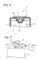
- the wiring connection portion 4a has a cantilever structure supported at one end only, namely at the bending or corner of the L shape. Therefore, when a large tensile external force shown by arrow F in Fig. 7, is imposed on an external wiring 8 having a connecting terminal metal part 9 fixed to the wiring connection portion 4a by means of a fixing screw 10 and the nut 7 as shown in Fig. 7, the wiring connection portion 4a is pulled in a direction indicated by an arrow P (turned clockwise in Fig. 7) and deformed as shown. This may happen to an extent that the wiring connection portion 4a is lifted with the nut 7 pulled out from the recess 5a.
- WO-A-91/15873 discloses a semiconductor device having an outer casing housing a semiconductor chip and filled with a sealing compound, several terminals bent into an L-shape of which one leg extends into the casing and is connected to the semiconductor chip while the other leg forms an external wiring connection portion disposed outside of the casing in parallel to a wall portion thereof, a recess formed in the wall portion beneath the wiring connection portion, and a terminal nut provided in the recess for connection of an external wiring to the wiring connection portion by means of a screw passing through a hole in the wiring connection portion and screwed into the terminal nut.
- the leg of the terminal extending into the casing is provided with recesses in which bosses or protruding portions forming part of the casing engage in a latching connection thereby blocking a vertical movement of the terminal leg extending vertically.
- JP-A-57-010952 the bending of lead terminals and correspondingly the damage of semiconductor elements upon application of a bending force to the connection portion of the terminal is avoided by injecting a resin such that the terminal nut for connecting the terminal by means of a screw passing through a hole in the terminal wiring connection portion is buried.
- US-A-3,995,932 discloses a convertible contact module for a relay including terminal straps which form closed loops at each end of the module housing.
- the legs formed in the terminal straps are firmly anchored to the module housing.
- This anchoring is obtained by inserting the two end portions of the leg sidewardly into respective slots provided in the base portion of the two-part housing, whereafter a cover comprising two projecting portions, which engage in the slots of the base and a respective recess between the end portion and the legs, is fastened to the base.
- the terminal strap is blocked or anchored in the base by means of the protruding portions of the cover latching by engaging with the recesses adjacent the respective end portions.
- the present invention has been made after considering these problems, with the intention of solving said problems, and its objective is to provide a terminal structure for such resin-sealed or potted semiconductor device with improved support strength against external forces acting on the external part of the terminal.
- an anchor that is bent downward is disposed on the tip of the terminal extending further from the external wiring connection portion, said anchor being fixed on the casing.
- the anchor may be fixed by inserting the tip of the anchor into the outer casing and embedding it in the sealing compound, or forming the tip of the anchor integrally with the outer casing by embedding it in the case lid that has been formed as a resin molding independent of the outer casing.
- an auxiliary metal anchoring member is inserted between the terminal nut and the external wiring connection portion of the terminal, the leg of said auxiliary member being fixed on the outer casing.
- the auxiliary member may be fixed by inserting a leg of the auxiliary member into the outer casing and embedding it in the molded resin serving as sealing compound.
- the external wiring connection portion of the terminal and the terminal nut, or the external wiring connection portion and the auxiliary metal anchoring member are bonded together by screwing the external wiring onto the wiring connection portion with a fixing screw.
- the wiring connection portion is fixed to the casing at two points thereby increasing the strength of the support. Therefore, even if a large tensile external force is imposed on an external wiring connection portion of the terminal via the external wiring, undesirable deformation of the terminal and its floating away from the outer casing can be prevented, and trouble such as breakage of the terminal can be reliably prevented even if a repeated load such as a vibration is imposed.
- Figs. 1 (a), (b) and (c) show a first embodiment of the invention which differs from the conventional device explained above mainly by having the terminal 4 equipped with a tongue-like anchor portion 4c formed and arranged to provide for a second support of the wiring connection portion 4a.
- the anchor portion 4c extends from the distal end of the wiring connection portion 4a, i.e. the end of the latter opposite to the end where it is bent from the lower part of the terminal 4.
- the anchor portion 4c is bent downward or back into the casing 5 through a hole 5b on the top of the outer casing 5.
- the free tip end of the anchor portion 4c is embedded and fixed in the sealing compound 6.
- Numeral 4d denotes an anchoring hole drilled at the tip of the anchor portion 4c.
- the above structure is assembled in the following manner: After the circuit assembly is covered with the casing 5, the terminal 4 protruding from the top of the casing 5 is bent into an inverted U-shape with the wiring connection portion 4a forming the base of the U-shape and located outside of the casing 5 and the anchor portion 4c inserted into the casing 5. Then the sealing compound or resin 6 is injected into the casing 5 and hardened. Thus, the rising lower part of the terminal 4 and at least the tip end of the anchor portion 4c are embedded and fixed in the sealing compound 6. By providing an anchoring hole 4d in the anchor portion 4c, sealing compound 6 will flow through this anchoring hole 4d, thereby increasing the bonding strength. This allows the wiring connection portion to be supported at two opposite sides, thus assuring a high support strength, and preventing the problems of the conventional semiconductor device mentioned above.
- Fig. 2 shows a second embodiment of the present invention.
- a case lid 11 made from resin separate from said casing 5 is provided on top of the casing.
- the terminal 4 has substantially the same structure as that of the first embodiment, however, in this case the upper part of the terminal 4 is formed integrally with the case lid such that, except for the wiring connection portion 4a, the upper part of the terminal 4 is embedded in the case lid 11.
- the case lid 11 is molded integrally with the terminal 4 and the terminal nut 7 before the terminal 4 is integrated into the circuit assembly and after the wiring connection portion 4a and the anchor portion 4c are bent and formed.
- a box nut is used as the terminal nut 7 to prevent resin from getting into the screw hole during the forming process.
- the terminal 4 now formed integrally with the case lid 11 is integrated into the circuit assembly, the circuit assembly covered with the casing 5 and the casing 5 filled with sealing compound 6, which is then hardened thereby securing the case lid 11 to the casing 5.
- This construction improves the supporting strength of the terminal 4 to the same extent as that in the first embodiment described earlier. Moreover, such a construction makes it possible to bend the terminal 4 prior to integrating it into the circuit assembly, thus making the assembling efficiency higher than in the first embodiment.
- Fig. 3 shows a third embodiment of the present invention.
- a separate metal anchoring member 12 which is bent into an L shape is inserted between the wiring connection portion 4a and the terminal nut 7.
- a bent leg 12a of this member 12 is inserted into the casing through a hole 5b in the outer casing 5 at a position opposite to where the terminal 4 comes out of the casing 5 and is embedded and fixed in the sealing compound 6 therein.
- Numeral 12b is a screw hole provided in the horizontal leg of the anchoring member 12 at a position registered with the terminal nut 7, and numeral 12c is an anchoring hole drilled at the tip of the leg 12a.
- Figs. 4 (a) through (e) show variations of the metal anchoring member 12 of Fig. 3.
- Notches 12d providing an equivalent anchoring effect are formed in place of the anchoring hole 12c in Figs. 4 (a) and (b), while irregular steps 12e are formed in Fig. 4 (c), and plural legs 12a are formed in Figs. 4 (d) and (e), each leg being provided with an anchoring hole 12c.
- the terminal can be reliably prevented from becoming excessively deformed and from being lifted off the outer casing, or from breaking due to a repeated load such as vibration, even if great external tensile force is applied to the external wiring screwed on the external wiring connection portion of the terminal. As a result, the product reliability can be greatly improved.
Landscapes
- Structures Or Materials For Encapsulating Or Coating Semiconductor Devices Or Solid State Devices (AREA)
- Connections Arranged To Contact A Plurality Of Conductors (AREA)
Claims (4)
- Halbleiterbauelement mit einem Außengehäuse (5), welches einen Halbleiterchip (3) beherbergt und mit einer Vergußmasse (6) gefüllt ist, wenigstens einem Anschluß (4), der in eine L-Form gebogen ist, deren einer Schenkel sich in das Gehäuse (5) erstreckt und mit dem Halbleiterchip (3) verbunden ist, während der andere Schenkel einen externen Verdrahtungsverbindungsabschnitt (4a) bildet, der außerhalb des Gehäuses (5) im wesentlichen parallel zu einem Wandabschnitt desselben angeordnet ist, einer Ausnehmung (5a), die in dem Wandabschnitt unterhalb des Verdrahtungsverbindungsabschnitts (4a) ausgebildet ist, und einer Anschlußmutter (7), die in der Ausnehmung (5a) zur Verbindung einer externen Verdrahtung (8, 9) mit dem Verdrahtungsverbindungsabschnitt (4a) mittels einer Schraube (10) vorgesehen ist, welche ein Loch in dem Verdrahtungsverbindungsabschnitt (4a) durchsetzt und in die Anschlußmutter (7) geschraubt ist,
gekennzeichnet durch Verankerungsmittel (4c, 12), die den Verdrahtungsverbindungsabschnitt (4a) an einer von der Ecke des L-förmigen Anschlusses (4) beabstandeten Position zusätzlich an dem Gehäuse (5) fixieren,
wobei die Verankerungsmittel (4c, 12) einen streifenförmigen, sich nach unten erstreckenden Ankerteil (4c, 12a) umfassen, der in das Gehäuse (5) eingesteckt und in der Vergußmasse (6) eingebettet ist, wobei der Ankerteil (4c, 12a) auf der dem einen Schenkel des Anschlusses (4) entgegengesetzten Seite des Lochs in dem Verdrahtungsverbindungsabschnitt (4a) positioniert ist. - Halbleiterbauelement nach Anspruch 1, bei dem der Ankerteil (4c) ein einstückiger Teil des Anschlusses (4) ist, der an dem der Ecke entgegengesetzten Ende des Verdrahtungsverbindungsabschnitts (4a) vorgesehen und nach unten gebogen ist.
- Halbleiterbauelement nach Anspruch 2, bei dem der Wandabschnitt des Gehäuses (5) von einem Gehäusedeckel (11) gebildet ist, das als gesondertes Harzformteil ausgebildet und mittels der Vergußmasse (6) an dem Gehäuse (5) fixiert ist, wobei die Spitze des Ankerteils (4c) integral in den Gehäusedeckel (11) eingesetzt ist anstatt in der Vergußmasse (6) eingebettet zu sein.
- Halbleiterbauelement nach Anspruch 1, bei dem die Verankerungsmittel ein gesondertes Verankerungsglied (12) umfassen, welches im wesentlichen L-förmig ist, wobei ein Schenkel zwischen dem Verdrahtungsverbindungsabschnitt (4a) und die Anschlußmutter (7) gesetzt ist und ein mit der Anschlußmutter (7) ausgerichtetes Schraubloch (12b) aufweist, während der andere Schenkel (12a), der den Ankerteil bildet, das Verankerungsglied (12) an dem Gehäuse (5) fixiert.
Applications Claiming Priority (2)
| Application Number | Priority Date | Filing Date | Title |
|---|---|---|---|
| JP265222/92 | 1992-10-05 | ||
| JP4265222A JPH06120390A (ja) | 1992-10-05 | 1992-10-05 | 樹脂封止形半導体装置の端子構造 |
Publications (3)
| Publication Number | Publication Date |
|---|---|
| EP0591900A2 EP0591900A2 (de) | 1994-04-13 |
| EP0591900A3 EP0591900A3 (de) | 1994-11-23 |
| EP0591900B1 true EP0591900B1 (de) | 1999-01-13 |
Family
ID=17414223
Family Applications (1)
| Application Number | Title | Priority Date | Filing Date |
|---|---|---|---|
| EP93116022A Expired - Lifetime EP0591900B1 (de) | 1992-10-05 | 1993-10-04 | In Harz versiegeltes Halbleiterbauelement |
Country Status (4)
| Country | Link |
|---|---|
| US (1) | US5373105A (de) |
| EP (1) | EP0591900B1 (de) |
| JP (1) | JPH06120390A (de) |
| DE (1) | DE69323025T2 (de) |
Families Citing this family (28)
| Publication number | Priority date | Publication date | Assignee | Title |
|---|---|---|---|---|
| JPH0969603A (ja) * | 1995-09-01 | 1997-03-11 | Mitsubishi Electric Corp | 電力用半導体装置、その外装ケースとその製造方法 |
| USD393829S (en) | 1995-09-27 | 1998-04-28 | Sony Corporation | Rechargeable battery |
| JP3168901B2 (ja) * | 1996-02-22 | 2001-05-21 | 株式会社日立製作所 | パワー半導体モジュール |
| USD413858S (en) * | 1998-05-29 | 1999-09-14 | Sony Corporation | Rechargeable battery |
| JP4151209B2 (ja) | 2000-08-29 | 2008-09-17 | 三菱電機株式会社 | 電力用半導体装置 |
| JP4092071B2 (ja) * | 2000-11-30 | 2008-05-28 | 三菱電機株式会社 | 半導体パワーモジュール |
| US6359785B1 (en) * | 2001-01-04 | 2002-03-19 | Chin-Feng Lin | Power diode and heat sink arrangement |
| JP4497803B2 (ja) * | 2002-09-20 | 2010-07-07 | 豊田鉄工株式会社 | 樹脂製部品の締結部構造 |
| JP3864130B2 (ja) * | 2002-10-10 | 2006-12-27 | 三菱電機株式会社 | 電力用半導体装置 |
| JP4607995B2 (ja) * | 2008-11-28 | 2011-01-05 | 三菱電機株式会社 | 電力用半導体装置 |
| JP5113815B2 (ja) * | 2009-09-18 | 2013-01-09 | 株式会社東芝 | パワーモジュール |
| DE102010000908B4 (de) * | 2010-01-14 | 2015-07-16 | Infineon Technologies Ag | Leistungshalbleitermodul mit niederinduktiven Hochstromkontakten, Leistungshalbleitermodulsystem, Leistungshalbleitermodulanordnung und Verfahren zur Herstellung einer Leisungshalbleitermodulanordnung |
| JP5359927B2 (ja) * | 2010-02-24 | 2013-12-04 | 株式会社デンソー | バスバーの締結構造および電力変換装置 |
| JP5476600B2 (ja) * | 2010-04-15 | 2014-04-23 | 三菱電機株式会社 | 半導体装置 |
| JP2014120657A (ja) * | 2012-12-18 | 2014-06-30 | Toshiba Corp | 半導体装置 |
| JP6299120B2 (ja) * | 2013-09-05 | 2018-03-28 | 富士電機株式会社 | 半導体モジュール |
| CA2927501C (en) * | 2013-10-16 | 2017-06-20 | Aleees Eco Ark Co. Ltd. | Positive locking confirmation mechanism for battery contact of electric vehicle |
| EP3203515B1 (de) * | 2014-09-30 | 2022-11-09 | Sansha Electric Manufacturing Co., Ltd. | Halbleitermodul mit gehäuse für verbesserte sichtprüfung |
| CN107205491A (zh) * | 2015-02-05 | 2017-09-26 | 菲利普莫里斯生产公司 | 具有锚定加热器的气溶胶生成装置 |
| WO2017017749A1 (ja) * | 2015-07-27 | 2017-02-02 | 三菱電機株式会社 | 半導体装置 |
| CN109959998B (zh) * | 2017-12-14 | 2024-05-14 | 新思考电机有限公司 | 透镜驱动装置、照相装置以及电子设备 |
| JP7354550B2 (ja) * | 2019-02-08 | 2023-10-03 | 富士電機株式会社 | 半導体モジュールの外部接続部、半導体モジュール、外部接続端子、および半導体モジュールの外部接続端子の製造方法 |
| JP7334485B2 (ja) * | 2019-06-07 | 2023-08-29 | 富士電機株式会社 | 半導体モジュールの外部接続部、半導体モジュールの外部接続部の製造方法、半導体モジュール、車両、及び外部接続部とバスバーとの接続方法 |
| JP2021077791A (ja) * | 2019-11-11 | 2021-05-20 | 株式会社デンソー | リアクトル |
| JP6797505B1 (ja) | 2020-03-23 | 2020-12-09 | 株式会社三社電機製作所 | 半導体装置 |
| JP7791436B2 (ja) * | 2022-03-28 | 2025-12-24 | ミネベアパワーデバイス株式会社 | パワー半導体モジュール及びそれを用いた電力変換装置 |
| JP2023169935A (ja) * | 2022-05-18 | 2023-12-01 | 矢崎総業株式会社 | コネクタ |
| JP2023176298A (ja) * | 2022-05-31 | 2023-12-13 | 富士電機株式会社 | 端子構造、端子構造の製造方法、及び半導体装置 |
Family Cites Families (20)
| Publication number | Priority date | Publication date | Assignee | Title |
|---|---|---|---|---|
| US3581266A (en) * | 1968-12-30 | 1971-05-25 | Lionel E Weyenberg | Housed resistor |
| DE1961042C3 (de) * | 1969-12-05 | 1981-01-15 | Robert Bosch Gmbh, 7000 Stuttgart | Halbleiterbauelement |
| US3648337A (en) * | 1970-08-24 | 1972-03-14 | Mallory & Co Inc P R | Encapsulating of electronic components |
| US3995932A (en) * | 1975-06-20 | 1976-12-07 | Allen-Bradley Company | Terminal for convertible contact module |
| FR2333362A1 (fr) * | 1975-11-26 | 1977-06-24 | Alsthom Cgee | Borne a vis a serrage sous tete |
| US4172272A (en) * | 1978-05-01 | 1979-10-23 | International Rectifier Corporation | Solid state relay having U-shaped conductive heat sink frame |
| DD141736B1 (de) * | 1979-03-19 | 1983-01-26 | Werner Friedrich | Klemmenanordnung an zweipoligen steckdosen |
| JPS5710952A (en) * | 1980-06-23 | 1982-01-20 | Mitsubishi Electric Corp | Resin sealed type semiconductor device |
| US4538168A (en) * | 1981-09-30 | 1985-08-27 | Unitrode Corporation | High power semiconductor package |
| US4443655A (en) * | 1981-11-27 | 1984-04-17 | Unitrode Corporation | Extruded semiconductor package and fabrication method |
| DE3370254D1 (en) * | 1982-11-29 | 1987-04-16 | Idec Izumi Corp | Wire terminal connector |
| EP0138048B1 (de) * | 1983-09-29 | 1993-12-15 | Kabushiki Kaisha Toshiba | Halbleiteranordnung in Druckpackung |
| GB2202994B (en) * | 1987-03-05 | 1991-04-24 | Seiko Epson Corp | Circuit assembly, e.g. for an electronic timepiece |
| JPH01106457A (ja) * | 1987-10-19 | 1989-04-24 | Mitsubishi Electric Corp | 樹脂封止形半導体装置 |
| US4880400A (en) * | 1988-02-24 | 1989-11-14 | Jacobson Mfg. Co., Inc. | Wire-wrap connector |
| JPH025559A (ja) * | 1988-06-24 | 1990-01-10 | Fuji Electric Co Ltd | 半導体装置 |
| JP2522511Y2 (ja) * | 1989-01-26 | 1997-01-16 | オムロン 株式会社 | 電気機器のシール構造 |
| FR2660826A1 (fr) * | 1990-04-05 | 1991-10-11 | Mcb Sa | Boitier economique pour composants electroniques de puissance, a fixer sur dissipateur thermique et son procede de fabrication. |
| GB2249869B (en) * | 1990-09-17 | 1994-10-12 | Fuji Electric Co Ltd | Semiconductor device |
| US5281493A (en) * | 1992-09-04 | 1994-01-25 | Globe-Union Inc. | Terminal construction for a battery |
-
1992
- 1992-10-05 JP JP4265222A patent/JPH06120390A/ja active Pending
-
1993
- 1993-10-04 EP EP93116022A patent/EP0591900B1/de not_active Expired - Lifetime
- 1993-10-04 US US08/130,714 patent/US5373105A/en not_active Expired - Fee Related
- 1993-10-04 DE DE69323025T patent/DE69323025T2/de not_active Expired - Lifetime
Also Published As
| Publication number | Publication date |
|---|---|
| DE69323025D1 (de) | 1999-02-25 |
| JPH06120390A (ja) | 1994-04-28 |
| EP0591900A3 (de) | 1994-11-23 |
| EP0591900A2 (de) | 1994-04-13 |
| DE69323025T2 (de) | 1999-07-15 |
| US5373105A (en) | 1994-12-13 |
Similar Documents
| Publication | Publication Date | Title |
|---|---|---|
| EP0591900A2 (de) | In Harz versiegeltes Halbleiterbauelement | |
| US4441119A (en) | Integrated circuit package | |
| CN109997221B (zh) | 半导体装置、控制装置以及半导体装置的制造方法 | |
| JP2001525126A (ja) | セラミック基板を備えた電力用半導体モジュール | |
| US5479050A (en) | Leadframe with pedestal | |
| CN105518851A (zh) | 半导体装置及其制造方法 | |
| US5175610A (en) | Resin molded type semiconductor device having a metallic plate support | |
| JP3975181B2 (ja) | 電力用半導体装置 | |
| US6147398A (en) | Semiconductor device package | |
| US6828600B2 (en) | Power semiconductor module with ceramic substrate | |
| US5691884A (en) | Semiconductor device with removably fixed lead frame | |
| EP0694966A1 (de) | Packung einer elektronischen Halbleiterschaltung | |
| US5557145A (en) | Mounting construction and method of a semiconductor device by which deformation of leads is prevented | |
| KR100371019B1 (ko) | 스마트 카드 | |
| KR20060051197A (ko) | 플라스틱 오버몰드 패키지용 리드프레임 디자인 | |
| JP2645852B2 (ja) | 電子装置 | |
| US20030205788A1 (en) | Leadframe assembly | |
| EP0069733A1 (de) | Integrierte schaltungseinheit | |
| KR0141945B1 (ko) | 방열판을 갖는 리드 프레임 및 이를 이용한 반도체 패키지 | |
| KR100575589B1 (ko) | 커플 본딩부를 구비한 빔 리드를 포함하는 에프비지에이패키지 | |
| KR100867571B1 (ko) | 전력용 반도체 모듈용 케이스 및 이를 이용한 전력용반도체 모듈의 제조 방법 | |
| KR200286323Y1 (ko) | 반도체패키지 | |
| KR200169730Y1 (ko) | 반도체 패키지의 리드프레임 | |
| KR200211272Y1 (ko) | 칩 사이즈 패키지 | |
| KR0156335B1 (ko) | 타이 바를 이용한 반도체 칩 패키지 |
Legal Events
| Date | Code | Title | Description |
|---|---|---|---|
| PUAI | Public reference made under article 153(3) epc to a published international application that has entered the european phase |
Free format text: ORIGINAL CODE: 0009012 |
|
| AK | Designated contracting states |
Kind code of ref document: A2 Designated state(s): DE FR GB |
|
| PUAL | Search report despatched |
Free format text: ORIGINAL CODE: 0009013 |
|
| AK | Designated contracting states |
Kind code of ref document: A3 Designated state(s): DE FR GB |
|
| 17P | Request for examination filed |
Effective date: 19950116 |
|
| 17Q | First examination report despatched |
Effective date: 19960415 |
|
| GRAG | Despatch of communication of intention to grant |
Free format text: ORIGINAL CODE: EPIDOS AGRA |
|
| GRAG | Despatch of communication of intention to grant |
Free format text: ORIGINAL CODE: EPIDOS AGRA |
|
| GRAH | Despatch of communication of intention to grant a patent |
Free format text: ORIGINAL CODE: EPIDOS IGRA |
|
| GRAH | Despatch of communication of intention to grant a patent |
Free format text: ORIGINAL CODE: EPIDOS IGRA |
|
| GRAA | (expected) grant |
Free format text: ORIGINAL CODE: 0009210 |
|
| AK | Designated contracting states |
Kind code of ref document: B1 Designated state(s): DE FR GB |
|
| REF | Corresponds to: |
Ref document number: 69323025 Country of ref document: DE Date of ref document: 19990225 |
|
| ET | Fr: translation filed | ||
| PLBE | No opposition filed within time limit |
Free format text: ORIGINAL CODE: 0009261 |
|
| STAA | Information on the status of an ep patent application or granted ep patent |
Free format text: STATUS: NO OPPOSITION FILED WITHIN TIME LIMIT |
|
| 26N | No opposition filed | ||
| REG | Reference to a national code |
Ref country code: GB Ref legal event code: IF02 |
|
| REG | Reference to a national code |
Ref country code: FR Ref legal event code: D6 |
|
| PGFP | Annual fee paid to national office [announced via postgrant information from national office to epo] |
Ref country code: FR Payment date: 20081014 Year of fee payment: 16 |
|
| PGFP | Annual fee paid to national office [announced via postgrant information from national office to epo] |
Ref country code: GB Payment date: 20081001 Year of fee payment: 16 |
|
| PGFP | Annual fee paid to national office [announced via postgrant information from national office to epo] |
Ref country code: DE Payment date: 20091001 Year of fee payment: 17 |
|
| REG | Reference to a national code |
Ref country code: FR Ref legal event code: ST Effective date: 20100630 |
|
| PG25 | Lapsed in a contracting state [announced via postgrant information from national office to epo] |
Ref country code: FR Free format text: LAPSE BECAUSE OF NON-PAYMENT OF DUE FEES Effective date: 20091102 |
|
| PG25 | Lapsed in a contracting state [announced via postgrant information from national office to epo] |
Ref country code: GB Free format text: LAPSE BECAUSE OF NON-PAYMENT OF DUE FEES Effective date: 20091004 |
|
| REG | Reference to a national code |
Ref country code: DE Ref legal event code: R119 Ref document number: 69323025 Country of ref document: DE Effective date: 20110502 |
|
| PG25 | Lapsed in a contracting state [announced via postgrant information from national office to epo] |
Ref country code: DE Free format text: LAPSE BECAUSE OF NON-PAYMENT OF DUE FEES Effective date: 20110502 |