EP0592084B1 - Procédé de fabrication d'un transistor Schottky avec une cathode de puit du type n rétrogradée et son procédé de fabrication - Google Patents
Procédé de fabrication d'un transistor Schottky avec une cathode de puit du type n rétrogradée et son procédé de fabrication Download PDFInfo
- Publication number
- EP0592084B1 EP0592084B1 EP93306385A EP93306385A EP0592084B1 EP 0592084 B1 EP0592084 B1 EP 0592084B1 EP 93306385 A EP93306385 A EP 93306385A EP 93306385 A EP93306385 A EP 93306385A EP 0592084 B1 EP0592084 B1 EP 0592084B1
- Authority
- EP
- European Patent Office
- Prior art keywords
- diode
- layer
- collector
- buried
- mask
- Prior art date
- Legal status (The legal status is an assumption and is not a legal conclusion. Google has not performed a legal analysis and makes no representation as to the accuracy of the status listed.)
- Expired - Lifetime
Links
- 238000004519 manufacturing process Methods 0.000 title claims description 47
- 238000000034 method Methods 0.000 title claims description 45
- 230000008569 process Effects 0.000 title claims description 37
- 229910052751 metal Inorganic materials 0.000 claims description 39
- 239000002184 metal Substances 0.000 claims description 39
- 239000007943 implant Substances 0.000 claims description 34
- 239000000758 substrate Substances 0.000 claims description 34
- 239000004065 semiconductor Substances 0.000 claims description 26
- 238000000151 deposition Methods 0.000 claims description 23
- 230000008021 deposition Effects 0.000 claims description 16
- BASFCYQUMIYNBI-UHFFFAOYSA-N platinum Chemical compound [Pt] BASFCYQUMIYNBI-UHFFFAOYSA-N 0.000 claims description 14
- 239000003870 refractory metal Substances 0.000 claims description 14
- 239000000463 material Substances 0.000 claims description 13
- 238000005530 etching Methods 0.000 claims description 9
- 238000002955 isolation Methods 0.000 claims description 8
- 229910052697 platinum Inorganic materials 0.000 claims description 7
- 125000006850 spacer group Chemical group 0.000 claims description 4
- ZXEYZECDXFPJRJ-UHFFFAOYSA-N $l^{3}-silane;platinum Chemical compound [SiH3].[Pt] ZXEYZECDXFPJRJ-UHFFFAOYSA-N 0.000 claims description 3
- 229910021339 platinum silicide Inorganic materials 0.000 claims description 3
- 238000005245 sintering Methods 0.000 claims description 2
- 230000008878 coupling Effects 0.000 claims 2
- 238000010168 coupling process Methods 0.000 claims 2
- 238000005859 coupling reaction Methods 0.000 claims 2
- 239000010410 layer Substances 0.000 description 131
- 125000004429 atom Chemical group 0.000 description 13
- 230000015572 biosynthetic process Effects 0.000 description 11
- 238000009792 diffusion process Methods 0.000 description 8
- 230000037361 pathway Effects 0.000 description 8
- 230000002441 reversible effect Effects 0.000 description 8
- 230000007423 decrease Effects 0.000 description 7
- 238000000137 annealing Methods 0.000 description 6
- 150000004767 nitrides Chemical class 0.000 description 6
- 125000004437 phosphorous atom Chemical group 0.000 description 6
- 239000011229 interlayer Substances 0.000 description 4
- 230000008901 benefit Effects 0.000 description 3
- 239000000969 carrier Substances 0.000 description 3
- 239000002131 composite material Substances 0.000 description 3
- 238000002513 implantation Methods 0.000 description 3
- 230000003647 oxidation Effects 0.000 description 3
- 238000007254 oxidation reaction Methods 0.000 description 3
- VYPSYNLAJGMNEJ-UHFFFAOYSA-N Silicium dioxide Chemical compound O=[Si]=O VYPSYNLAJGMNEJ-UHFFFAOYSA-N 0.000 description 2
- 230000003247 decreasing effect Effects 0.000 description 2
- 238000005137 deposition process Methods 0.000 description 2
- 238000005247 gettering Methods 0.000 description 2
- 230000003071 parasitic effect Effects 0.000 description 2
- 238000002161 passivation Methods 0.000 description 2
- 238000003860 storage Methods 0.000 description 2
- ZOXJGFHDIHLPTG-UHFFFAOYSA-N Boron Chemical group [B] ZOXJGFHDIHLPTG-UHFFFAOYSA-N 0.000 description 1
- 229910052581 Si3N4 Inorganic materials 0.000 description 1
- XUIMIQQOPSSXEZ-UHFFFAOYSA-N Silicon Chemical compound [Si] XUIMIQQOPSSXEZ-UHFFFAOYSA-N 0.000 description 1
- 239000000370 acceptor Substances 0.000 description 1
- WATWJIUSRGPENY-UHFFFAOYSA-N antimony atom Chemical group [Sb] WATWJIUSRGPENY-UHFFFAOYSA-N 0.000 description 1
- RQNWIZPPADIBDY-UHFFFAOYSA-N arsenic atom Chemical group [As] RQNWIZPPADIBDY-UHFFFAOYSA-N 0.000 description 1
- 230000004888 barrier function Effects 0.000 description 1
- 230000015556 catabolic process Effects 0.000 description 1
- 239000003795 chemical substances by application Substances 0.000 description 1
- 238000005229 chemical vapour deposition Methods 0.000 description 1
- 230000000295 complement effect Effects 0.000 description 1
- 239000013078 crystal Substances 0.000 description 1
- 230000000593 degrading effect Effects 0.000 description 1
- 230000001419 dependent effect Effects 0.000 description 1
- 230000000694 effects Effects 0.000 description 1
- 230000008030 elimination Effects 0.000 description 1
- 238000003379 elimination reaction Methods 0.000 description 1
- 238000005468 ion implantation Methods 0.000 description 1
- 210000003127 knee Anatomy 0.000 description 1
- 230000004807 localization Effects 0.000 description 1
- 150000002739 metals Chemical group 0.000 description 1
- 230000004048 modification Effects 0.000 description 1
- 238000012986 modification Methods 0.000 description 1
- 229910021420 polycrystalline silicon Inorganic materials 0.000 description 1
- 238000002360 preparation method Methods 0.000 description 1
- 230000009467 reduction Effects 0.000 description 1
- 229910021332 silicide Inorganic materials 0.000 description 1
- 229910052710 silicon Inorganic materials 0.000 description 1
- 239000010703 silicon Substances 0.000 description 1
- 235000012239 silicon dioxide Nutrition 0.000 description 1
- 239000000377 silicon dioxide Substances 0.000 description 1
- HQVNEWCFYHHQES-UHFFFAOYSA-N silicon nitride Chemical compound N12[Si]34N5[Si]62N3[Si]51N64 HQVNEWCFYHHQES-UHFFFAOYSA-N 0.000 description 1
- 238000005382 thermal cycling Methods 0.000 description 1
- 238000007740 vapor deposition Methods 0.000 description 1
Images



Classifications
-
- H—ELECTRICITY
- H10—SEMICONDUCTOR DEVICES; ELECTRIC SOLID-STATE DEVICES NOT OTHERWISE PROVIDED FOR
- H10D—INORGANIC ELECTRIC SEMICONDUCTOR DEVICES
- H10D84/00—Integrated devices formed in or on semiconductor substrates that comprise only semiconducting layers, e.g. on Si wafers or on GaAs-on-Si wafers
- H10D84/60—Integrated devices formed in or on semiconductor substrates that comprise only semiconducting layers, e.g. on Si wafers or on GaAs-on-Si wafers characterised by the integration of at least one component covered by groups H10D10/00 or H10D18/00, e.g. integration of BJTs
- H10D84/611—Combinations of BJTs and one or more of diodes, resistors or capacitors
- H10D84/613—Combinations of vertical BJTs and one or more of diodes, resistors or capacitors
- H10D84/617—Combinations of vertical BJTs and only diodes
Definitions
- the present invention relates to an improved a process for fabricating a Schottky transistor structure incorporating a retrograde localized well under an extended base contact, establishing a Schottky diode structure in conjunction with the bipolar transistor structure.
- the present invention is applicable to bipolar and BICMOS integrated circuits, with fabrication processes that lead to faster, more reliable Schottky transistor structures. More particularly, the present invention uses selected mask sequences from bipolar fabrication steps with modification of the masks according to the invention to form the improved Schottky transistor.
- donor concentrations in the epitaxial layer can vary by as much as ⁇ 30% from semiconductor "wafer" to wafer, or within a wafer. In prior-art structures these variations resulted from the way in which donor concentrations were achieved; that is, the growth of the epitaxial layer controlled the donor levels in the wafer. In fact, actual donor concentrations in the epitaxial layer are not known until after the deposition process is completed. This fluctuation translates into characteristic variability for a given fabrication lot; it directly affects the forward voltage drop and the reverse current at the metal-semiconductor interface. It also directly affects the series resistance through the bulk of the epitaxial layer. In effect, the forward voltage drop, the reverse current leakage rate, and the series resistance may all vary significantly from one diode to the next.
- the present invention adds to and enhances the bipolar transistor fabrication process by including the fabrication of the retrograde diode well in the active area of the transistor.
- the retrograde well enhances the portion of the epitaxial layer in the region underlying the Schottky contact area. This is of importance in the particular bipolar fabrication process contemplated for as previously stated, the epitaxial layer of the present invention is very lightly doped and a Schottky diode using such an epitaxial layer as its substrate would require a higher-than-desirable turn-on voltage, and it would have a very high series resistance.
- the next major step in the process is to form the transistor's sub-emitter collector region by using a sub-emitter collector definition mask, etch and implant sequence to implant relatively fast-diffusing N type atoms in a portion of the buried collector layer.
- the retrograde diode well is fabricated by constructing the sub-emitter collector definition mask to act not only as a sub-emitter collector definition mask, but as a retrograde diode well definition mask also, with a retrograde diode well defining opening over the buried diode layer of the improved bipolar structure.
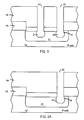
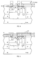
- Figure 3 is a simplified diagrammatic elevation view of the 2.0 mask, etch and implant sequence of the bipolar transistor fabrication process showing the new 2.0 sub-emitter collector definition mask with bipolar transistor sub-emitter collector region opening and the new retrograde diode well definition opening for the Schottky diode structure of the Schottky transistor structure described in the preferred embodiment of the present invention.
- Mask Function 1.0 Buried Collector Layer (BCL) Mask 2.0 Retro Sub-Emitter Collector (SEC) Mask 3.0 Channel Stop (CHST) Mask 4.0 Isolation Oxide (ISOX) Mask 5.0 Sink Implant & ISOX Gettering Mask 6.0 Field Oxide Mask & Collector Base Surface Spacer (CBSS) Definition Mask 7.0 Active Strip Mask 9.0 Base Definition Mask 10.0 Nitride Etch Mask or Collector Base & Emitter Contact Definition Mask 11.0 Emitter & Collector Sink Implant Mask (Self-Aligned Transistor Mask) 14.0 Contact Definition Mask 15.0 Metal 1 (M1) Deposition Mask 16.0 VIA Mask (Inter Layer Dielectric Mask) 17.0 Metal 2 (M2) Deposition Mask 18.0 Passivation Mask
- a new SEC photo-resist layer 19 is deposited to form the 2.0 retro SEC definition mask.
- the new 2.0 mask is formed to provide a sub-emitter collector region definition mask with an SEC opening 20 for the formation of a sub-emitter collector region 21 of said bipolar transistor structure 7 . It also provides a retrograde diode well definition mask with a retrograde diode well opening 22 over a buried diode region 23 of said expanded buried collector layer 11 for said Schottky diode structure 8 . Relatively fast-diffusing Phosphorus atoms are implanted to an N + concentration through the new 2.0 mask to form, among other sub-elements, said retrograde diode well 9 .
- a new 2.0 SEC mask may be formed to provide only said retrograde diode well definition mask with said retrograde diode well opening 22 , thereby eliminating the formation of said sub-emitter collector region 21 .
Landscapes
- Electrodes Of Semiconductors (AREA)
- Bipolar Transistors (AREA)
- Bipolar Integrated Circuits (AREA)
Claims (7)
- Procédé de fabrication d'une structure de transistor Schottky ayant une structure de transistor bipolaire (7) et une structure de diode Schottky (8), la structure de transistor bipolaire ayant des régions de collecteur de base (30) et d'émetteur (38) formées dans la surface d'une couche épitaxiale (13) de matière semiconductrice déposée sur un substrat et une couche de collecteur enterrée formée dans le substrat sous-jacent aux régions de collecteur, de base et d'émetteur, la couche de collecteur enterrée étant séparée des régions de base et d'émetteur par une partie de la couche épitaxiale, dans lequel la fabrication de la diode Schottky comporte des étapes dans la séquence suivante consistant à :
- a.
- former une couche de diode enterrée (11) en implantant des atomes de type N dans le substrat à travers une ouverture de masque de définition de couche de diode enterrée pendant une séquence de masquage de définition de couche de collecteur enterrée bipolaire ;
- b.
- former un puits de diode rétrograde (9) en implantant des atomes de type N à travers une ouverture de masque de définition de puits de diode rétrograde et jusque dans la couche de diode enterrée ;
- c.
- déposer ladite couche épitaxiale (13) sur la couche de diode enterrée et le puits de diode rétrograde et à diffuser le puits de diode vers le haut jusqu'à la surface de la couche épitaxiale ;
- d.
- former une région de contact de jonction de diode (37) par-dessus le puits de diode rétrograde en déposant une couche de couverture de métal réfractaire sur la couche épitaxiale et en attaquant le métal réfractaire tout en laissant un contact de jonction de diode en métal réfractaire pendant une séquence de masquage de définition de contact bipolaire ; et
- e.
- former un contact métallique par-dessus le contact de jonction de diode pendant une séquence de masquage de définition de contact en premier métal bipolaire.
- Procédé selon la revendication 1, dans lequel le transistor bipolaire (7) a une région de récepteur de courant de collecteur formée dans la couche épitaxiale couplant électriquement la région de collecteur avec la couche de collecteur enterrée et une région de collecteur de sous-émetteur formée dans la couche de collecteur enterrée s'étendant jusqu'à la région de collecteur enterrée et couplant la région de base électriquement avec celle-ci, la structure de transistor Schottky est isolée de structures adjacentes par des régions d'oxyde isolant, une région d'espacement collecteur / surface de base sépare le collecteur de la base, et il y a des régions de contact intégrées au niveau des surfaces des régions de collecteur, de base et d'émetteur ; et dans lequel le procédé bipolaire comporte les étapes consistant à :
- a.
- former la couche de collecteur enterrée de la structure de transistor bipolaire dans le substrat en utilisant la séquence de masquage de définition de couche de collecteur enterrée, d'attaque et d'implantation pour implanter des premiers atomes de type N à travers une ouverture de définition de couche de collecteur enterrée du masque de définition de couche de collecteur enterrée et jusque dans le substrat ;
- b.
- former la région de récepteur de courant de collecteur de la structure de transistor bipolaire dans la couche épitaxiale par-dessus la couche de collecteur enterrée en utilisant une séquence de masquage de définition de région de récepteur de courant de collecteur, d'attaque et d'implantation pour implanter des atomes de type N à diffusion relativement rapide à travers une ouverture de définition de récepteur de courant de collecteur du masque de définition de récepteur de courant de collecteur ;
- c.
- former les régions de contact bipolaire intégrées de la structure de transistor bipolaire en utilisant une séquence de masquage de définition de contacts de transistor bipolaire, d'attaque et de dépôt pour déposer une couverture de métal réfractaire sur la structure de transistor bipolaire et attaquer le métal réfractaire à travers des ouvertures de définition de contacts bipolaires du masque de définition de contacts bipolaires de manière à former des régions de contact de structure de transistor bipolaire ; et
- d.
- former des contacts en premier métal de la structure de transistor bipolaire en utilisant la séquence de masquage de définition et d'attaque de premier métal pour former les contacts en premier métal à travers des ouvertures de définition de contacts en premier métal du masque de définition de premier métal ;
- a.
- construire ledit masque de définition de couche de collecteur enterrée également en tant que masque de définition de couche de diode enterrée avec une ouverture de définition de couche de diode enterrée par-dessus ledit substrat et implanter lesdits atomes de type N à travers ladite ouverture de définition de couche enterrée tout en formant ladite couche de collecteur enterrée ;
- b.
- former ledit puits de diode rétrograde dans ladite couche épitaxiale en utilisant une séquence de masquage de définition de puits de diode rétrograde, d'attaque et d'implantation pour implanter des atomes de type N à travers une ouverture de définition de puits de diode rétrograde dudit masque de définition de puits de diode rétrograde ;
- c.
- construire le masque de définition de contacts bipolaires également en tant que masque de définition de contact de jonction de diode avec des ouvertures de définition de jonction de diode par-dessus le puits de diode rétrograde, déposer la couverture de métal réfractaire sur l'ouverture de définition de contact de jonction de diode et attaquer le métal réfractaire à travers l'ouverture de définition de contact de jonction de diode tout en attaquant la couverture de métal réfractaire pour former les régions de contact de la structure de transistor bipolaire ; et
- d.
- construire le masque de définition de premier métal également en tant que masque de définition de premier métal de diode avec une ouverture de définition de premier métal de diode par-dessus la jonction de diode pour former un contact en premier métal de diode tout en formant les contacts en premier métal de la structure de transistor bipolaire.
- Procédé selon la revendication 2, comportant, en outre, l'étape consistant à former la région de collecteur de sous-émetteur de la structure de transistor bipolaire en utilisant une séquence de masquage de définition de région de collecteur de sous-émetteur, d'attaque et d'implantation pour implanter des atomes de type N à travers une ouverture de définition de région de collecteur de sous-émetteur du masque de définition de région de collecteur de sous-émetteur et à construire le masque de définition de région de collecteur de sous-émetteur également en tant que masque de définition de puits de diode rétrograde avec l'ouverture de définition de puits de diode rétrograde par-dessus la couche de diode enterrée et à implanter les atomes de type N à travers l'ouverture de définition de puits de diode rétrograde tout en formant la région de collecteur de sous-émetteur de la structure de transistor bipolaire.
- Procédé selon la revendication 1 ou la revendication 2, dans lequel le métal réfractaire est le platine.
- Procédé selon la revendication 4, dans lequel la jonction de diode est formée en frittant le platine sur une surface du puits de diode rétrograde de manière à former une jonction platine-siliciure.
- Procédé selon la revendication 2, comportant, en outre, l'étape consistant à modifier l'ouverture de définition de couche de collecteur enterrée du masque de définition de couche de collecteur enterrée pour inclure l'ouverture de définition de couche de diode enterrée de telle sorte que la couche de collecteur enterrée et la couche de diode enterrée forment une seule couche de collecteur enterrée agrandie.
- Procédé selon la revendication 2, comportant, en outre, l'étape consistant à modifier une ouverture de contact de base du masque de définition de contacts bipolaires pour inclure l'ouverture de définition de jonction de diode de telle sorte que le contact de base et la jonction de diode forment un seul contact de base agrandi.
Applications Claiming Priority (2)
| Application Number | Priority Date | Filing Date | Title |
|---|---|---|---|
| US94903592A | 1992-09-22 | 1992-09-22 | |
| US949035 | 1992-09-22 |
Publications (2)
| Publication Number | Publication Date |
|---|---|
| EP0592084A1 EP0592084A1 (fr) | 1994-04-13 |
| EP0592084B1 true EP0592084B1 (fr) | 1998-01-07 |
Family
ID=25488503
Family Applications (1)
| Application Number | Title | Priority Date | Filing Date |
|---|---|---|---|
| EP93306385A Expired - Lifetime EP0592084B1 (fr) | 1992-09-22 | 1993-08-12 | Procédé de fabrication d'un transistor Schottky avec une cathode de puit du type n rétrogradée et son procédé de fabrication |
Country Status (5)
| Country | Link |
|---|---|
| US (1) | US5536966A (fr) |
| EP (1) | EP0592084B1 (fr) |
| JP (1) | JPH06236989A (fr) |
| KR (1) | KR100303701B1 (fr) |
| DE (1) | DE69316134T2 (fr) |
Families Citing this family (6)
| Publication number | Priority date | Publication date | Assignee | Title |
|---|---|---|---|---|
| US5631495A (en) * | 1994-11-29 | 1997-05-20 | International Business Machines Corporation | High performance bipolar devices with plurality of base contact regions formed around the emitter layer |
| US6013936A (en) | 1998-08-06 | 2000-01-11 | International Business Machines Corporation | Double silicon-on-insulator device and method therefor |
| EP2323164B1 (fr) * | 2000-08-14 | 2015-11-25 | SanDisk 3D LLC | Matrice de mémoire à niveaux multiples et son procédé de fabrication |
| US7157785B2 (en) * | 2003-08-29 | 2007-01-02 | Fuji Electric Device Technology Co., Ltd. | Semiconductor device, the method of manufacturing the same, and two-way switching device using the semiconductor devices |
| KR100763848B1 (ko) * | 2006-07-05 | 2007-10-05 | 삼성전자주식회사 | 쇼트키 다이오드 및 그 제조 방법 |
| US8759194B2 (en) | 2012-04-25 | 2014-06-24 | International Business Machines Corporation | Device structures compatible with fin-type field-effect transistor technologies |
Family Cites Families (7)
| Publication number | Priority date | Publication date | Assignee | Title |
|---|---|---|---|---|
| JPS58166765A (ja) * | 1982-03-27 | 1983-10-01 | Toshiba Corp | 半導体装置の製造方法 |
| US4982244A (en) * | 1982-12-20 | 1991-01-01 | National Semiconductor Corporation | Buried Schottky clamped transistor |
| JPS59177960A (ja) * | 1983-03-28 | 1984-10-08 | Hitachi Ltd | 半導体装置およびその製造方法 |
| US4498227A (en) * | 1983-07-05 | 1985-02-12 | Fairchild Camera & Instrument Corporation | Wafer fabrication by implanting through protective layer |
| JPS6281120A (ja) * | 1985-10-03 | 1987-04-14 | Fujitsu Ltd | 半導体装置 |
| US4849344A (en) * | 1986-12-11 | 1989-07-18 | Fairchild Semiconductor Corporation | Enhanced density modified isoplanar process |
| EP0500233A2 (fr) * | 1991-02-14 | 1992-08-26 | National Semiconductor Corporation | Structure de transistor bipolaire et méthode de fabrication BICMOS IC |
-
1993
- 1993-08-12 DE DE69316134T patent/DE69316134T2/de not_active Expired - Lifetime
- 1993-08-12 EP EP93306385A patent/EP0592084B1/fr not_active Expired - Lifetime
- 1993-09-21 KR KR1019930019112A patent/KR100303701B1/ko not_active Expired - Lifetime
- 1993-09-22 JP JP5236734A patent/JPH06236989A/ja active Pending
-
1994
- 1994-08-15 US US08/290,684 patent/US5536966A/en not_active Expired - Lifetime
Also Published As
| Publication number | Publication date |
|---|---|
| US5536966A (en) | 1996-07-16 |
| DE69316134D1 (de) | 1998-02-12 |
| EP0592084A1 (fr) | 1994-04-13 |
| KR940008111A (ko) | 1994-04-28 |
| JPH06236989A (ja) | 1994-08-23 |
| DE69316134T2 (de) | 1998-06-18 |
| KR100303701B1 (ko) | 2001-11-22 |
Similar Documents
| Publication | Publication Date | Title |
|---|---|---|
| KR100200059B1 (ko) | 쇼트키 장벽 다이오드 및 쇼트키 장벽 다이오드 클램프형 트랜지스터와 이들을 제조하는 방법 | |
| US5119162A (en) | Integrated power DMOS circuit with protection diode | |
| JP2689047B2 (ja) | 絶縁ゲート型バイポーラトランジスタとその製造方法 | |
| JP3202785B2 (ja) | モノリシック半導体装置及びその製造方法 | |
| US5344785A (en) | Method of forming high speed, high voltage fully isolated bipolar transistors on a SOI substrate | |
| US5124271A (en) | Process for fabricating a BiCMOS integrated circuit | |
| US5565701A (en) | Integrated circuit with vertical bipolar power transistors and isolated lateral bipolar control transistors | |
| US5583348A (en) | Method for making a schottky diode that is compatible with high performance transistor structures | |
| KR100196484B1 (ko) | 얇은 희생층을 사용하여 수직형 퓨즈 디바이스 및 쇼트키다이오드를 제조하는 방법 | |
| US5139961A (en) | Reducing base resistance of a bjt by forming a self aligned silicide in the single crystal region of the extrinsic base | |
| US4982244A (en) | Buried Schottky clamped transistor | |
| JPS61210662A (ja) | 半導体構成体 | |
| US5268316A (en) | Fabrication process for Schottky diode with localized diode well | |
| US5212102A (en) | Method of making polysilicon Schottky clamped transistor and vertical fuse devices | |
| EP0043007B1 (fr) | Structure de circuit à transistors bipolaires à saturation limitée et méthode de fabrication correspondante | |
| EP0233202A1 (fr) | Fabrication d'un dispositif a semi-conducteur avec de l'oxyde enfoui. | |
| US5218227A (en) | Semiconductor device and method of manufacturing same | |
| US5536966A (en) | Retrograde NWell cathode Schottky transistor and fabrication process | |
| EP0545521B1 (fr) | Structure de diode schottky et procédé de fabrication | |
| US5298440A (en) | Method of fabrication of transistor device with increased breakdown voltage | |
| US5013671A (en) | Process for reduced emitter-base capacitance in bipolar transistor | |
| EP0178968B1 (fr) | Logique à transistors à couplage de base | |
| US5242854A (en) | High performance semiconductor devices and their manufacture | |
| US5506156A (en) | Method of fabricating bipolar transistor having high speed and MOS transistor having small size | |
| JP2845469B2 (ja) | 半導体装置 |
Legal Events
| Date | Code | Title | Description |
|---|---|---|---|
| PUAI | Public reference made under article 153(3) epc to a published international application that has entered the european phase |
Free format text: ORIGINAL CODE: 0009012 |
|
| AK | Designated contracting states |
Kind code of ref document: A1 Designated state(s): DE FR GB IT NL |
|
| 17P | Request for examination filed |
Effective date: 19941010 |
|
| 17Q | First examination report despatched |
Effective date: 19941031 |
|
| GRAG | Despatch of communication of intention to grant |
Free format text: ORIGINAL CODE: EPIDOS AGRA |
|
| GRAG | Despatch of communication of intention to grant |
Free format text: ORIGINAL CODE: EPIDOS AGRA |
|
| GRAH | Despatch of communication of intention to grant a patent |
Free format text: ORIGINAL CODE: EPIDOS IGRA |
|
| GRAH | Despatch of communication of intention to grant a patent |
Free format text: ORIGINAL CODE: EPIDOS IGRA |
|
| GRAA | (expected) grant |
Free format text: ORIGINAL CODE: 0009210 |
|
| AK | Designated contracting states |
Kind code of ref document: B1 Designated state(s): DE FR GB IT NL |
|
| PG25 | Lapsed in a contracting state [announced via postgrant information from national office to epo] |
Ref country code: NL Free format text: LAPSE BECAUSE OF FAILURE TO SUBMIT A TRANSLATION OF THE DESCRIPTION OR TO PAY THE FEE WITHIN THE PRESCRIBED TIME-LIMIT Effective date: 19980107 Ref country code: IT Free format text: LAPSE BECAUSE OF FAILURE TO SUBMIT A TRANSLATION OF THE DESCRIPTION OR TO PAY THE FEE WITHIN THE PRE;WARNING: LAPSES OF ITALIAN PATENTS WITH EFFECTIVE DATE BEFORE 2007 MAY HAVE OCCURRED AT ANY TIME BEFORE 2007. THE CORRECT EFFECTIVE DATE MAY BE DIFFERENT FROM THE ONE RECORDED.SCRIBED TIME-LIMIT Effective date: 19980107 Ref country code: FR Free format text: LAPSE BECAUSE OF FAILURE TO SUBMIT A TRANSLATION OF THE DESCRIPTION OR TO PAY THE FEE WITHIN THE PRESCRIBED TIME-LIMIT Effective date: 19980107 |
|
| REF | Corresponds to: |
Ref document number: 69316134 Country of ref document: DE Date of ref document: 19980212 |
|
| NLV1 | Nl: lapsed or annulled due to failure to fulfill the requirements of art. 29p and 29m of the patents act | ||
| EN | Fr: translation not filed | ||
| PG25 | Lapsed in a contracting state [announced via postgrant information from national office to epo] |
Ref country code: GB Free format text: LAPSE BECAUSE OF NON-PAYMENT OF DUE FEES Effective date: 19980812 |
|
| PLBE | No opposition filed within time limit |
Free format text: ORIGINAL CODE: 0009261 |
|
| STAA | Information on the status of an ep patent application or granted ep patent |
Free format text: STATUS: NO OPPOSITION FILED WITHIN TIME LIMIT |
|
| 26N | No opposition filed | ||
| GBPC | Gb: european patent ceased through non-payment of renewal fee |
Effective date: 19980812 |
|
| PGFP | Annual fee paid to national office [announced via postgrant information from national office to epo] |
Ref country code: DE Payment date: 20110830 Year of fee payment: 19 |
|
| REG | Reference to a national code |
Ref country code: DE Ref legal event code: R082 Ref document number: 69316134 Country of ref document: DE |
|
| PG25 | Lapsed in a contracting state [announced via postgrant information from national office to epo] |
Ref country code: DE Free format text: LAPSE BECAUSE OF NON-PAYMENT OF DUE FEES Effective date: 20130301 |
|
| REG | Reference to a national code |
Ref country code: DE Ref legal event code: R119 Ref document number: 69316134 Country of ref document: DE Effective date: 20130301 |