EP0592842B1 - Conversion de fréquence sérielle qui peut tolérer une faible instabilité de phase de la charge utile - Google Patents
Conversion de fréquence sérielle qui peut tolérer une faible instabilité de phase de la charge utile Download PDFInfo
- Publication number
- EP0592842B1 EP0592842B1 EP93115140A EP93115140A EP0592842B1 EP 0592842 B1 EP0592842 B1 EP 0592842B1 EP 93115140 A EP93115140 A EP 93115140A EP 93115140 A EP93115140 A EP 93115140A EP 0592842 B1 EP0592842 B1 EP 0592842B1
- Authority
- EP
- European Patent Office
- Prior art keywords
- clock rate
- format
- serial
- low
- circuit
- Prior art date
- Legal status (The legal status is an assumption and is not a legal conclusion. Google has not performed a legal analysis and makes no representation as to the accuracy of the status listed.)
- Expired - Lifetime
Links
Images

Classifications
-
- H—ELECTRICITY
- H04—ELECTRIC COMMUNICATION TECHNIQUE
- H04J—MULTIPLEX COMMUNICATION
- H04J3/00—Time-division multiplex systems
- H04J3/02—Details
- H04J3/12—Arrangements providing for calling or supervisory signals
-
- H—ELECTRICITY
- H04—ELECTRIC COMMUNICATION TECHNIQUE
- H04J—MULTIPLEX COMMUNICATION
- H04J3/00—Time-division multiplex systems
- H04J3/16—Time-division multiplex systems in which the time allocation to individual channels within a transmission cycle is variable, e.g. to accommodate varying complexity of signals, to vary number of channels transmitted
- H04J3/1605—Fixed allocated frame structures
- H04J3/1611—Synchronous digital hierarchy [SDH] or SONET
-
- H—ELECTRICITY
- H04—ELECTRIC COMMUNICATION TECHNIQUE
- H04J—MULTIPLEX COMMUNICATION
- H04J2203/00—Aspects of optical multiplex systems other than those covered by H04J14/05 and H04J14/07
- H04J2203/0001—Provisions for broadband connections in integrated services digital network using frames of the Optical Transport Network [OTN] or using synchronous transfer mode [STM], e.g. SONET, SDH
- H04J2203/0057—Operations, administration and maintenance [OAM]
- H04J2203/0058—Network management, e.g. Intelligent nets
-
- H—ELECTRICITY
- H04—ELECTRIC COMMUNICATION TECHNIQUE
- H04J—MULTIPLEX COMMUNICATION
- H04J2203/00—Aspects of optical multiplex systems other than those covered by H04J14/05 and H04J14/07
- H04J2203/0001—Provisions for broadband connections in integrated services digital network using frames of the Optical Transport Network [OTN] or using synchronous transfer mode [STM], e.g. SONET, SDH
- H04J2203/0089—Multiplexing, e.g. coding, scrambling, SONET
Definitions
- the present invention is generally directed to electronics and more specifically to serial data flowrate conversion circuits. Even more specifically, the present invention is directed to an approach for converting the rate of serial link data back and forth between a high-rate that uses a high-rate data frame and low-rate that uses a low-rate data frame in a way that does not transform the data into a parallel format and that centers the low-rate data frame as a payload within the high-rate data frame to provide jitter tolerance.
- SONET synchronous optical network
- SONET defines a standard optical interface that allows mid-span meets between equipment produced by different manufacturers. Therefore, the rate conversion of SONET clock rate-derived data to a clock rate suitable for data communication integrated circuits is and for some time to come will be a common operation in telecommunication systems. To accomplish this, it is necessary to rate convert serial streams containing multiple 8-bit time slots from one clock rate to another in dual directions with a minimal amount of circuitry. A principal focus of such an approach would be to provide an implementation that is tolerate of long- or short-term variation in the clock signals.
- An example is the ability to convert numerous data communication channels that are embedded in a SONET overhead data link (ODL) from a higher data flowrate of 6.48 Mb/s to a lower data communications channel (DCC) integrated circuit data flowrate of 4.096 Mb/s with tolerance for jitter that may arise from the conversion process.
- ODL SONET overhead data link
- DCC data communications channel
- U.S. Patent No. 4,839,893 discloses a telecommunications FIFO that provides an interface between two serial data transmission channels which have independent clocks and which can operate according to different protocols.
- the FIFO contains two storage registers each equal to a frame of data in length. Data is written into and read form alternate storage registers with the transfer between one register and the other occurring upon the receipt of write and read frame sync pulses respectively.
- the read address location and the write address location respectively are sampled to determine if a FIFO overfill or empty condition is eminent. If such condition exists, the telecommunications FIFO does not switch registers, but rather rewrites the same register or rereads the same register respectively, to thereby perform a slip operation.
- GB 2 050 119 A discloses a data processing apparatus with multiplexer/ demultiplexer systems.
- a data stream is clocked at a variable rate into a buffer memory.
- the data is clocked out at a rate into a second, higher rate data stream.
- bit positions are assigned for a minimum number of bits, which are always transferred, and additional data bits, which may or may not be transferred, depending on the occupancy of the memory.
- a counter serves as an occupancy detector for the memory.
- the output of the associated register which is indicative of whether or not additional bits are to be used, increments and decrements an up/ down counter when additional bits are and are not used.
- a multiplexer combines in the second stream the data bits, a code indicating whether the additional bits are used or not and a code giving the number in the counter.
- information derived at the demultiplexer from previous values of the cumulative total and stored in a rate memory is used to provide additional bits to the data stream at approximately the correct frequency.
- the cumulative total transmitted in the next frame is used to restore the bit count integrity of the data stream.
- serial rate conversion circuits use dual port RAMs or FIFOs. These circuits convert the data from serial to parallel and back to serial in the rate conversion process.
- the payload traffic in these solutions is usually not tolerate of jitter or wander in the clock signals. Consequently, traffic often will be lost if any short- or long-term variation arises from the rate conversion.
- the present approach overcomes these limitations by providing rate conversion of serial link data without transforming the data into parallel and by centering the payload of the low-speed interface within the high-speed frame for providing jitter tolerance.
- a significant reduction between 20 and 40%) in component count and board space results for an equivalent number of serial links as compared to conventional parallel solutions using dual port RAMs and FIFOs.
- the overhead data link (ODL)operating at 6.48 Mb/s (megabits per second) is converted to the data communications channel (DCC) rate of 4.096 Mb/s and vice-versa to permit serial data links on the two sides of the circuit to operate at different rates.
- DCC data communications channel
- the implementation may also be easily expanded to rate convert more than eight serial links by width expanding the separate input/output RAM devices.
- the present approach more specifically is to convert the clock rate of a serial stream of signals between the ODL clock rate and the DCC clock rate.
- the circuit of the present conception has a first memory and address select circuit that communicates a stream of serial formatted signals at the ODL clock rate.
- a second memory and address select circuit communicates the stream of serial formatted signals at the DCC clock rate.
- the circuit includes clock rate converting components associated between the first memory and address circuit and the second memory and address select circuit to convert the stream of serial formatted signals between the ODL data rate and the DCC data rate while maintaining the stream in the serial format.
- the circuit of the present invention communicates a signal stream in an ODL serial format associated with the ODL rate circuit.
- the ODL serial format has 101 1/4 bytes inclusive from a beginning byte 1 through an ending byte 101 1/4.
- the approach also requires communicating the signal stream in a DCC serial format associated with the DCC rate circuit.
- the DCC serial format has 64 bytes including DCC byte 1 through DCC byte 64.
- the approach is to continuously translate between the ODL and DCC frames by associating each of the DCC bytes elements with one of the ODL bytes so that the beginning DCC byte (or DCC byte 1) associates with the ODL frame serially at a position after the beginning ODL byte (i.e., after ODL byte 1) and the ending DCC byte (i.e., DCC byte 64) associates serially before the ending ODL byte (i.e., before ODL byte 101 1/4).
- the DCC frame is embedded within or cushioned by the ODL frame.
- the present invention converts signals from data communications channels which are embedded in a SONET overhead from a high-speed rate which is a typical SONET overhead data link (ODL) rate of 6.48 Mb/s to the typical data communication channel (DCC) data flowrate of 4.096 Mb/s.
- ODL SONET overhead data link
- DCC data communication channel
- the 4.096 Mb/s rate is a rate that is very common to DCC integrated circuits.
- the preferred embodiment permits routing data from a central RTSI board to other sub-boards at a normal DCC integrated circuit serial rate.
- the present invention makes it is possible to fit within a standard European 6U printed circuit board all circuitry necessary to convert the SONET ODL serial rate of 6.48 Mb/s to the normal DCC serial rate of 4.096 Mb/s.
- the preferred embodiment directly reads into a RAM location and then reads the data serially at the effective clock rate.
- the preferred embodiment permits two-way flow of serial signal streams from a rate of 6.48 Mb/s to a rate of 4.096 Mb/s, and vice-versa.
- the approach is to take from the 6.48 Mb/s side 512 bits within a possible 810 bits and then center the 512 bits as a low-speed payload or frame within the high-speed side payload or frame.
- the preferred embodiment permits synchronization with an 8-KHz external phase lock loop.
- An external phase lock loop locks on the frame boundaries and, in the preferred embodiment, operates at a frequency of 8-KHz to provide a clocking signal every 125 microseconds for adjusting the two rates of the high-speed and low-speed sides. If data loss occurs due to synchronization, it occurs around the frame boundaries. By centering the low-speed payload-within the high-speed frame, i.e., not having the low-speed payload at either the beginning or the end of the frame, the chance of losing data due to phase lock loop synchronization adjustment is significantly reduced.
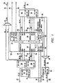
- 1 serial rate conversion circuit 10 of the preferred embodiment appears as a schematic block diagram. Beginning at eight individual data bit links 12 to latch 14, a 4.096-Mb/s clock signal 16 is received and an RTSI RSDDC link comes into serial rate conversion circuit 10. The low data flowrate payload from link 12 is to be centered within the high data flowrate payload.
- the eight bit lines of link 12 are totally separate and are not related in any way. Although the preferred embodiment uses eight separate bit lines into latch 14, it is possible to size the circuit differently. Therefore, link 12 may include eight bit lines, five bit lines, or whatever would be desired for a particular application.
- Latch 14 latches the data coming in and associates the data with 4.096-Mb/s clock signal at input 16 to exactly position the data at the boundary of the clock. As such, latch 14 avoids problems with external interfaces not being aligned to a specific 4.096-Mb/s clock boundary.
- RAM bank 26 and RAM bank 28 From latch 14, 4.096 Mb/s serial signals go to RAM bank 26 and RAM bank 28. While signals, for example, are written to RAM bank 26, RAM 28 sends out data in ODL frames for 6.48-Mb/s serial rate data. When RAM bank 26 is filled, the functions of RAM bank 26 and 28 switch so that RAM bank 28 receives the serial signal stream from latch 14, and RAM 26 outputs signals in a 6.48-Mb/s serial frame. Output 32 for RAM bank 26 and output 42 for RAM bank 28, respectively, provide data when RAM bank 26 is being read from or RAM bank 28 is being read from. From lines 32 and 42, 6.48-Mb/s payload data is logically multiplexed through multiplex path 30 to output 44.
- the preferred embodiment sends 6.48-Mb/s ODL signals to a large cross-connect ASIC ("application specific integrated circuit") that acts as the central SONET control circuit.
- Address connects 36 and 46 go, respectively, to RAM banks 26 and 28.
- Chip select bits 40 and 50 respectively, control chip selection for RAM banks 26 and 28.
- Address decode field programmable gate (FPGA) array 52 provides the decode signals for both RAM banks 26 and 28 on the 4.096-Mb/s side and RAM banks 68 and 70 on the 6.48-Mb/s side.
- Address decode field programmable gate array 52 includes two internal counters.
- Counter 54 is a 6.48 Mb/s counter.
- Counter 58 is a 4.096-Mb/s counter. These counters, respectively, provide information to bank and address select circuits 34 and 56. In relation to the frame for the 4.096-Mb/s side, counter 58 runs one bit faster.
- Counter 58 receives a 4.096-Mb/s clock signal from clock input 18 and an 8-KHz 4.096-Mb/s sync signal from input 20.
- Counter 54 receives a 6.48-Mb/s clock signal from input 62 and an 8-KHz synchronous signal from input 64.
- a 6.48-Mb/s input data at input 66 goes to RAM bank 68 and RAM bank 70 in parallel.
- RAM bank 68 From RAM bank 68, 4.096-Mb/s data goes along bit lines 72 to DCC data logical multiplexer 74.
- the 4.096-Mb/s data also comes from RAM bank 70 from bit lines 78.
- RAM banks 68 and 70 operate in the switching manner similar to that of RAM banks 26 and 28.
- Address control for RAM bank 68 comes from bank and address select circuit 56 along bit lines 82.
- Write control signals from bank and address select circuit 56 to RAM bank 68 travel along bit line 84.
- Chip select control is carried from bank and address select circuit 56 to RAM bank 68 via chip select bit 86.
- RAM bank 70 receives address control signals along the nine bits 88 from bank and address select circuit 56. Write control signals go to RAM bank 70 via write bit 90, and chip select bit 92 provides control signals from bank and address circuit 56 to RAM bank 70. From DCC data multiplexer 74, 4.096-Mb/s data goes to data latch 24. This data is clocked out through output 94 to the appropriate DCC integrated circuit.
- the same nine address bits as represented by bits 36 and 46 connect, respectively, to RAM banks 26 and 28. These same bits are never turned on in exactly the same way at the same time. Only one of the write bits will be enabled at any given moment. The other RAM bank will have the chip select bit enabled only and will cause data to be read out of the RAM bank. Thus, when RAM bank 26 has its write enable bit 38 turned on, latch 14 writes data into RAM bank 26. At that same time, RAM bank 28 will have its chip select bit 50 enabled. This causes data to be read out of RAM bank 28 to logical multiplexer 30 via line 42. The same type of operation applies for writing data into RAM bank 28 and reading data from RAM bank 26.
- the address data on the nine bits at 36 and 46 contain incremental count signals that permit writing into the associated RAM bank beginning at location 0 and continuing sequentially through location 511. For example, if location 511 of RAM bank 26 is written to the RAM bank the selection of RAM banks will switch. This causes write enable bit 38 to turn off, write enable bit 48 to turn on, chip select bit 40 to turn on and chip select bit 50 to turn off. This causes 6.48-Mb/s serial signals that RAM bank 26 stores to go along bit 32 to logical multiplexer 30.
- Address decode FPGA 52 controls the operation of RAM banks 26 and 28 on the side that converts the 4.096-Mb/s DCC serial data rate to 6.48-Mb/s SONET ODL serial data rate. Address decode FPGA 52 also controls operation of RAM banks 68 and 70 to convert 6.48-Mb/s ODL serial signals to 4.096-Mb/s DCC signals.
- the preferred embodiment uses a rate conversion circuit consisting of a programmed Actel 1020A FPGA as address decode FPGA 52 and eight separate I/O SRAMs to reorganize the data frames between the ODL and DCC frame formats in both directions (i.e. in a full duplex mode).
- Two-bit delay circuit 60 permits lining up the data frames for sending data offboard. It is desirable to have this one bit advance, because this data is latched with the 4.096-Mb/s clock. If the data is one bit early getting it to the external latch, then the data is perfectly aligned after being clocked one more time. When going out upon coming back from the other board, the other board inserts two bits of delay. Therefore, the circuit permits catching the frame two bits later with regard to the 4.096 Mb/s side of circuit 10. With this approach, the preferred embodiment properly aligns the 4.096 Mb/s frame for the 6.48 Mb/s side so that the 6.48 Mb/s side is perfectly aligned with the SONET overhead data link in both the transmit and receive directions.
- the 6.48 Mb/s counter 54 is preset to 664 decimal when the 6.48 Mb/s frame sync occurs.
- the 6.48 Mb/s frame sync occurs 10 bits prior the start of the ODL frame.
- data is read from one bank of RAM the outputs of the other bank are set in a high impedance state.
- the outputs of the two banks are tied together and routed to both the ASICs as ODL inputs.
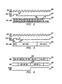
- FIGURE 2 shows the timing and formats of the overhead data link that the preferred embodiment uses.
- waveform 100 shows the 6.48 Mb/s ODL clock waveform.
- Waveform 104 illustrates the 8-KHz ODL synchronous or reference clock signal, and format 108 shows the ODL format to illustrate the end of the last bit 809 of an ODL frame at bit 106 and the beginning of byte 0 of ODL frame 108 at 110.
- the ODL sync signal 104 occurs 10 bits before the first byte 110 of ODL frame 108. Placing the ODL frame sync 10 bits before the first frame of the SONET frame is a matter of convention. This permits ASICs that decode on the high-speed side of the circuit to consistently have a place where the ODL sync signals occur.
- the 8-KHz sync signal identifies where a frame begins and provides an identifier for the location of bit 1 of the ODL frame.
- FIGURE 3 shows the waveforms for the 4.096 Mb/s DCC clock at waveform 112, the 8-KHz synchronous signal at waveform 116 and the frame format for the DCC data link at frame 120.
- the data communications channel sync occurs one-bit before the start of the frame.
- 8-KHz sync signal 114 occurs at bit 118 before DCC byte 1 at 122. Therefore, by DCC sync 114 occurring at bit 118, the beginning of DCC link frame 120 is identified.
- FIGURE 4 shows the DCC/ODL link interface timing relationship for the serial rate conversion circuit 10 of the preferred embodiment.
- FIGURE 4 shows the timing of the ODL and DCC links.
- the rising-edge of the phase lock loop 8-KHz reference signal which occurs every 125 microseconds marks the beginning of both the ODL and DCC frames.
- the bits in an ODL frame are numbered 0-809, and the bits in a DCC frame are numbered 0-511.
- the ODL frame appears as frame 124
- the DCC frame appears as frame 128, and the phase lock loop 8-KHz reference signal appears as waveform 132 in FIGURE 4.
- ODL frame 124 shows ODL bits 808, 809, 0 and 1 and 118 and identifies the beginning of the ODL frame at point 126.
- Frame 128 shows the DCC frame beginning between DCC bit 511 and DCC bit 0 at point 130.
- the phase lock loop 8-KHz reference signal waveform 132 reference signal turns on, both the ODL frame 124 and DCC frame 128 begin.
- ODL frame 124 is aligned with DCC frame 128.
- From the 8-KHz reference signal the actual DCC sync signal is provided via circuitry as is the ODL sync signal. But all signals are based on the phase lock loop 8-KHz external reference signal.
- FIGURE 5 provides a conceptual illustration of the ODL frame format.
- the ODL frame consist of 101 1/4 bytes. There are 99 valid bytes and 2 1/4 unused bytes at the end of the frame or 810 bits of information.
- the preferred embodiment positions the DCC payload within the ODL frame.
- the DCC payload consists of 64 valid bytes or 512 bits.
- FIGURE 6 shows how the preferred embodiment embeds the DCC 64 bytes within the 101 1/4 bytes of the ODL format. By placing the first DCC bytes at 17 bytes into the ODL frame, there are unused bits both before and after the DCC frame.
- ODL bytes 18-82 for example, of the ODL frame to be valid and to contain the 64 DCC bytes the preferred embodiment buffers around the DCC frame.
- the phase lock loop reference signal as indicated by waveform 132 of FIGURE 4
- An important technical advantage of the present invention is that it achieves serial rate conversion with between a 20 and 40% lower component count and associated board space than that of conventional serial rate conversion circuits. Therefore, for converting between the 6.48 Mb/s ODL data rate to the 4.096 Mb/s DCC data rate, it is possible to use standard 6U European boards that accommodate the numerous desired SONET applications.
- One difference between the present inventive approach and that of conventional circuits is that the preferred embodiment does not perform parity checks on a bit basis within individual lengths during the conversion process. This is not a significant limitation, because serial-to-parallel conversion does not take place in the circuit of the preferred embodiment.
- a parallel conversion is made, it is easy to use a ninth bit to parity check the consistency of other bits within the frame. Since integrity of the data is checked normally at both ends with a cyclic redundancy check (CRC) or other error checking methods, if an error is not detected during the rate conversion process, it is caught on one end of the other two boards in an associated subsystem. As such, because the preferred embodiment does not perform a parity check on a bit basis, this does not significantly impact operation of serial rate conversion circuit 10.
- CRC cyclic redundancy check
- the preferred embodiment receives at the eight input bits 12 the 4.096 Mb/s data and sends the bits to latch 14 along with a 4.096 Mb/s clock signal at clock signal input 16 of FIGURE 1.
- data is read into RAMs bank 26 or 28, depending on the control provided by the associated address decode FPGA 52 through write enable bits 38 and 48 and chip select bits 40 and 50.
- address bits 36 control the location of RAM bank 26 into which the DCC data is read. Once location 511 is filled in RAM bank 26, the 8-KHz external phase lock loop reference signal will cause the write enable bit 38 to turn off and chip select bit 40 to turn on. At the same time, write enable bit 48 will turn on and chip select bit 50 will turn off. This will cause latch 14 to write DCC 4.096 Mb/s data into RAM bank 28. With chip select enable bit 40 turned on, RAM bank 26 will send 6.48 Mb/s data out from link 32 to logical multiplexer 30. From logical multiplexer 30, 6.48 MB/s ODL frame data will go from rate conversion circuit 10 along 8-bit 6.48 Mb/s output 44.
- the serial rate conversion circuit 10 of the preferred embodiment operates by receiving the ODL data at input 66. Directly from input 66, data will go either to RAM bank 68 or 70. Assuming that data first goes to RAM bank 68, nine address bits 82 will control the location into which data is read into RAM bank 68. Write enable bit 84 then turns on and chip select bit 86 turns off. Conversely, address bits 88 switch address source, write enable bit 90 turns off and chip select bit 92 turns on. Any data that is in RAM-bank 70 will be sent via bit 78 to logical multiplexer 74 to be output as DCC data to latch 24.
- Latch 24 receives a 4.096 Mb/s clock signal at clock input 22 and outputs DCC data via bits 80 to external circuitry.
- phase lock loop 8-KHz reference signal causes write enable bit 84 to turn off, chip select bit 86 to turn on and data to be output via output bits 72 to logical multiplexer 74. From logical multiplexer 74, data goes to latch 24 to be output at 4.096 Mb/s output bits 80.
Landscapes
- Engineering & Computer Science (AREA)
- Computer Networks & Wireless Communication (AREA)
- Signal Processing (AREA)
- Time-Division Multiplex Systems (AREA)
- Dc Digital Transmission (AREA)
- Television Systems (AREA)
- Synchronisation In Digital Transmission Systems (AREA)
- Stabilization Of Oscillater, Synchronisation, Frequency Synthesizers (AREA)
- Optical Communication System (AREA)
Claims (13)
- Procédé pour communiquer des signaux entre un circuit à fréquence d'horloge élevée (66) et un circuit à fréquence d'horloge faible (12) et pour fournir une tolérance à l'instabilité, caractérisé par les étapes consistant à :communiquer un train série dans un format série à débit de données élevé (108) associé à un circuit à fréquence d'horloge élevée (66), ledit format série à débit de données élevé (108) possédant un premier nombre prédéterminé d'éléments à format à débit de données élevé (110) comprenant un élément à format à débit de données élevé de début (110) et un élément à format à débit de données élevé de fin (106) ;communiquer ledit train de signal dans un format série à débit de données faible (120) associé à un circuit à fréquence d'horloge faible (12), ledit format série à débit de données faible (120) possédant un nombre prédéterminé d'éléments à format de débit de données faible (118), comprenant un élément à format à débit de données faible de début (122) et un élément à format à débit de données faible de fin (1128), ledit nombre prédéterminé d'éléments à format de débit de données élevé (106) étant supérieur au nombre prédéterminé d'éléments à format à débit de données faible (118) ;convertir de manière continue ledit train série entre ledit format série à débit de données faible (120) et ledit format série à débit de données élevé (108) en associant chacun des éléments à format à débit de données faible (110) à l'un des éléments de données à format à débit de données élevé (110) de telle sorte que ledit élément à format de débit de données de début (122) s'associe audit format série à débit de données élevé (108) à une position qui soit située séquentiellement après ledit élément à format à débit de données élevé de début (110) et de telle sorte que ledit élément à format à débit de données faible de fin (118) s'associe à un élément à format à débit de données élevé (106) à une position qui soit située séquentiellement avant ledit élément à format à débit de données élevé de fin (106) ; et à convertir de manière continue le train série entre le format série à débit de données élevé et le format série à débit de données faible en associant chacun des éléments à format à débit de données élevé (106) avec un élément à format à débit de données faible (118).
- Procédé pour communiquer des signaux entre un circuit à fréquence d'horloge élevée (66) et un circuit à fréquence d'horloge faible (12) et pour fournir une tolérance à l'instabilité selon la revendication 1, comprenant en outre les étapes consistant à :communiquer une trame ODL de données (108) dans un train série associé à un circuit à débit de données ODL (66), ladite trame ODL (108) possédant plus de 99 octets valides comprenant un octet ODL 0 à un octet ODL 98 ;communiquer ledit train de signal dans une trame DCC (120) associée à un circuit à débit de données DCC (12), ledit format DCC possédant 64 octets comprenant un octet DCC 0 à un octet DCC 63 ;convertir de manière continue chaque train de signal entre ladite trame ODL (106) et ladite trame DCC (120) en associant chacun desdits octets DCC (122) à l'un desdits octets ODL (110) de telle sorte que ledit octet DCC 0 s'associe à ladite trame ODL (108) à une position qui soit située séquentiellement après ledit octet ODL 0 et de telle sorte que ledit octet DCC 64 s'associe à une position qui soit séquentiellement située avant ledit octet ODL 98 ;
età convertir de manière continue le train de signal entre la trame ODL (106) et la trame DCC (120) en associant chacun des octets ODL (110) avec l'un des octets DCC (122). - Procédé pour communiquer des signaux entre un circuit à fréquence d'horloge élevée (66) et_un circuit à fréquence d'horloge faible (12) et pour fournir une tolérance à l'instabilité selon la revendication 1 ou 2, comprenant en outre l'étape consistant à :recevoir des signaux de commande d'adresse (36, 46, 82, 88) .
- Procédé pour communiquer des signaux entre un circuit à fréquence d'horloge élevée (66) et un circuit à fréquence d'horloge faible (12) et pour fournir une tolérance à l'instabilité selon l'une quelconque des revendications 1 à 3, comprenant en outre l'étape consistant à :avancer des données (60) d'au moins un bit, moyennant quoi les trames de données sont alignées.
- Procédé pour communiquer des signaux entre un circuit à fréquence d'horloge élevée (66) et un circuit à fréquence d'horloge faible (12) et pour fournir une tolérance à l'instabilité selon l'une quelconque des revendications 1 à 4, comprenant en outre les étapes consistant à :compter (54, 58) au moins un signal d'horloge ; età compter (54, 58) au moins un signal synchrone.
- Procédé pour communiquer des signaux entre un circuit à fréquence d'horloge élevée (66) et un circuit à fréquence d'horloge faible (12) et pour fournir une tolérance à l'instabilité selon l'une quelconque des revendications 1 à 5, comprenant en outre l'étape consistant à :verrouiller (14) les données entrantes.
- Procédé pour communiquer des signaux entre un circuit à fréquence d'horloge élevée (66) et un circuit à fréquence d'horloge faible (12) et pour fournir une tolérance à l'instabilité selon l'une quelconque des revendications 1 à 6, comprenant en outre l'étape consistant à :multiplexer (30, 74) les données provenant d'au moins l'une desdites mémoires à fréquence d'horloge (26, 28, 68, 70) .
- Circuit de conversion de débit série (10) pour convertir un signal à débit de données élevé en un signal à débit de données faible, caractérisé par :une mémoire à fréquence d'horloge élevée (68 et 70) et un circuit de sélection d'adresse (56) pour stocker et communiquer un train série à format série à fréquence d'horloge élevée (108) associé à un circuit à fréquence d'horloge élevée (66), ledit format série à fréquence d'horloge élevée (108) possédant un premier nombre prédéterminé d'éléments à format à fréquence d'horloge élevée (110), comprenant un élément à format à fréquence d'horloge élevée de début (110) et un élément à format à fréquence d'horloge élevée de fin (106) ;une mémoire à fréquence d'horloge faible (26 et 28) et un circuit de sélection d'adresse (34) pour stocker et communiquer ledit train série dans un format série à fréquence d'horloge faible (120) associé à un circuit à fréquence d'horloge faible (12), ledit format série à fréquence d'horloge faible (120) possédant un deuxième nombre prédéterminé d'éléments à format série à fréquence d'horloge faible (122), comprenant un élément à format à fréquence d'horloge faible de début (122) et un élément à format à fréquence d'horloge faible de fin (118), et ledit premier nombre prédéterminé d'éléments à format à fréquence d'horloge élevée (110) étant supérieur audit deuxième nombre prédéterminé d'éléments à format à fréquence d'horloge faible (122) ; etun moyen de conversion (52) pour convertir de manière continue lesdits éléments à format série à fréquence d'horloge faible (120) et lesdits éléments à format à fréquence d'horloge élevée (122) en associant chacun des éléments à fréquence d'horloge faible (118) avec l'un des éléments à format à fréquence d'horloge élevée (110) de telle sorte que ledit élément à format à fréquence d'horloge faible de début (122) s'associe avec ledit format série à fréquence d'horloge élevée (108) à une position qui soit située séquentiellement après ledit élément à format à fréquence d'horloge élevée de début (110) et de telle sorte que ledit élément à format à fréquence d'horloge faible de fin (118) s'associe à une position qui soit située séquentiellement avant ledit élément à format à fréquence d'horloge élevée de fin (106), et dans lequel ledit moyen de conversion peut en outre fonctionner pour convertir de manière continue les éléments à format à fréquence d'horloge élevée en éléments à format à fréquence d'horloge faible en associant chacun des éléments à format à fréquence d'horloge élevée avec l'un des éléments à format à fréquence d'horloge faible.
- Circuit de conversion de débit série (10) pour convertir un signal à débit de données élevé en un signal à débit de données faible selon la revendication 8, comprenant en outre :des premières lignes de bits (82, 88) couplées audit circuit de sélection d'adresse (56) ; etdes deuxièmes lignes de bits (36, 46) couplées audit circuit de sélection d'adresse (34).
- Circuit de conversion de débit série (10) pour convertir un signal à débit de données élevé en un signal à débit de données faible selon la revendication 8 ou 9, comprenant en outre :un circuit à retard (60) couplé au moins à l'un desdits circuits de sélection d'adresse (34, 56), moyennant quoi des trames de données sont alignées.
- Circuit de conversion de débit série (10) pour convertir un signal à débit de données élevé en un signal à débit de données faible selon l'une quelconque des revendications 8 à 10, comprenant en outre :au moins un compteur (54, 58) couplé au moins à l'un desdits circuits de sélection d'adresse (34, 56).
- Circuit de conversion de débit série (10) pour convertir un signal à débit de données élevé en un signal à débit de données faible selon l'une quelconque des revendications 8 à 11, comprenant en outre :au moins un verrouillage (14) couplé au moins à l'une desdites mémoires à fréquence d'horloge (26, 28).
- Circuit de conversion de débit série (10) pour convertir un signal à débit de données élevé en un signal à débit de données faible selon l'une quelconque des revendications 8 à 12, comprenant en outre :au moins un multiplexeur (30, 74) couplé au moins à l'une desdites mémoires à fréquence d'horloge (26, 28, 68, 70).
Applications Claiming Priority (2)
| Application Number | Priority Date | Filing Date | Title |
|---|---|---|---|
| US07/962,319 US5425062A (en) | 1992-10-16 | 1992-10-16 | Serial rate conversion circuit with jitter tolerant payload |
| US962319 | 1992-10-16 |
Publications (3)
| Publication Number | Publication Date |
|---|---|
| EP0592842A2 EP0592842A2 (fr) | 1994-04-20 |
| EP0592842A3 EP0592842A3 (en) | 1996-03-06 |
| EP0592842B1 true EP0592842B1 (fr) | 2004-01-14 |
Family
ID=25505702
Family Applications (1)
| Application Number | Title | Priority Date | Filing Date |
|---|---|---|---|
| EP93115140A Expired - Lifetime EP0592842B1 (fr) | 1992-10-16 | 1993-09-21 | Conversion de fréquence sérielle qui peut tolérer une faible instabilité de phase de la charge utile |
Country Status (5)
| Country | Link |
|---|---|
| US (1) | US5425062A (fr) |
| EP (1) | EP0592842B1 (fr) |
| AT (1) | ATE257990T1 (fr) |
| DE (1) | DE69333381T2 (fr) |
| ES (1) | ES2210233T3 (fr) |
Families Citing this family (4)
| Publication number | Priority date | Publication date | Assignee | Title |
|---|---|---|---|---|
| US5692159A (en) * | 1995-05-19 | 1997-11-25 | Digital Equipment Corporation | Configurable digital signal interface using field programmable gate array to reformat data |
| US6198720B1 (en) * | 1996-12-26 | 2001-03-06 | Alcatel Usa Sourcing, L.P. | Distributed digital cross-connect system and method |
| KR100251736B1 (ko) * | 1997-12-29 | 2000-04-15 | 윤종용 | 직렬 데이터의 전송속도 변환 장치 |
| US6928573B2 (en) * | 2001-11-20 | 2005-08-09 | Broadcom Corporation | Communication clocking conversion techniques |
Family Cites Families (3)
| Publication number | Priority date | Publication date | Assignee | Title |
|---|---|---|---|---|
| US4229815A (en) * | 1978-11-20 | 1980-10-21 | Bell Telephone Laboratories, Incorporated | Full duplex bit synchronous data rate buffer |
| US4259738A (en) * | 1979-05-18 | 1981-03-31 | Raytheon Company | Multiplexer system providing improved bit count integrity |
| US4839893A (en) * | 1987-10-05 | 1989-06-13 | Dallas Semiconductor Corporation | Telecommunications FIFO |
-
1992
- 1992-10-16 US US07/962,319 patent/US5425062A/en not_active Expired - Lifetime
-
1993
- 1993-09-21 ES ES93115140T patent/ES2210233T3/es not_active Expired - Lifetime
- 1993-09-21 EP EP93115140A patent/EP0592842B1/fr not_active Expired - Lifetime
- 1993-09-21 DE DE69333381T patent/DE69333381T2/de not_active Expired - Fee Related
- 1993-09-21 AT AT93115140T patent/ATE257990T1/de not_active IP Right Cessation
Also Published As
| Publication number | Publication date |
|---|---|
| ES2210233T3 (es) | 2004-07-01 |
| EP0592842A3 (en) | 1996-03-06 |
| EP0592842A2 (fr) | 1994-04-20 |
| DE69333381D1 (de) | 2004-02-19 |
| ATE257990T1 (de) | 2004-01-15 |
| DE69333381T2 (de) | 2004-10-14 |
| US5425062A (en) | 1995-06-13 |
Similar Documents
| Publication | Publication Date | Title |
|---|---|---|
| US5142529A (en) | Method and means for transferring a data payload from a first SONET signal to a SONET signal of different frequency | |
| CA2130473C (fr) | Methode et appareil de resynchronisation et de conversion des signaux sts-1 en signaux sts-3 | |
| US5257261A (en) | Methods and apparatus for concatenating a plurality of lower level SONET signals into higher level sonet signals | |
| US6496540B1 (en) | Transformation of parallel interface into coded format with preservation of baud-rate | |
| US8942263B2 (en) | Data transmission in an SDH network | |
| US20100265953A1 (en) | Method and apparatus for signal splitting and combining | |
| US6820159B2 (en) | Bus interface for transfer of SONET/SDH data | |
| JPH02226926A (ja) | 多重チャネルpcmタイプのリング上にhdlcフレームを伝送するためのシステム | |
| EP1142241B1 (fr) | Systeme de communication et procedes de redressement associes | |
| US4839893A (en) | Telecommunications FIFO | |
| US7486703B2 (en) | Communications system with symmetrical interfaces and associated methods | |
| US6775294B2 (en) | Time slot assigner for communication system | |
| US5341492A (en) | Frame conversion circuit including initial value input circuit | |
| EP1142242B1 (fr) | Systeme de communication et procedes de redressement correspondants | |
| US5425062A (en) | Serial rate conversion circuit with jitter tolerant payload | |
| EP0543327B1 (fr) | Système synchrone de multiplexage optique | |
| US6208648B1 (en) | Network element and input/output device for a synchronous transmission system | |
| US6330237B1 (en) | Time slot assignment circuit | |
| US4712217A (en) | System for transmitting digital information and maintaining a minimum paulse density | |
| US4943958A (en) | ISDN interface trunk circuit | |
| JPH04506142A (ja) | データのスイッチングノード | |
| EP0713346A1 (fr) | Procédé et circuit pour connecter des dispositifs ATM/FDDI à des dispositifs ATM/SDH | |
| Kansal et al. | Enhanced satellite bandwidth utilization by optimum integration of split trunks and transcoders | |
| GB2330273A (en) | SDH network | |
| CA2229335A1 (fr) | Element de reseau et unite d'entree/de sortie pour un systeme de transmission synchrone |
Legal Events
| Date | Code | Title | Description |
|---|---|---|---|
| PUAI | Public reference made under article 153(3) epc to a published international application that has entered the european phase |
Free format text: ORIGINAL CODE: 0009012 |
|
| AK | Designated contracting states |
Kind code of ref document: A2 Designated state(s): AT BE CH DE ES FR GB IT LI NL SE |
|
| PUAL | Search report despatched |
Free format text: ORIGINAL CODE: 0009013 |
|
| AK | Designated contracting states |
Kind code of ref document: A3 Designated state(s): AT BE CH DE ES FR GB IT LI NL SE |
|
| RHK1 | Main classification (correction) |
Ipc: H04J 3/16 |
|
| 17P | Request for examination filed |
Effective date: 19960517 |
|
| 17Q | First examination report despatched |
Effective date: 20000310 |
|
| GRAH | Despatch of communication of intention to grant a patent |
Free format text: ORIGINAL CODE: EPIDOS IGRA |
|
| GRAS | Grant fee paid |
Free format text: ORIGINAL CODE: EPIDOSNIGR3 |
|
| GRAA | (expected) grant |
Free format text: ORIGINAL CODE: 0009210 |
|
| RAP1 | Party data changed (applicant data changed or rights of an application transferred) |
Owner name: ALCATEL |
|
| AK | Designated contracting states |
Kind code of ref document: B1 Designated state(s): AT BE CH DE ES FR GB IT LI NL SE |
|
| PG25 | Lapsed in a contracting state [announced via postgrant information from national office to epo] |
Ref country code: NL Free format text: LAPSE BECAUSE OF FAILURE TO SUBMIT A TRANSLATION OF THE DESCRIPTION OR TO PAY THE FEE WITHIN THE PRESCRIBED TIME-LIMIT Effective date: 20040114 Ref country code: LI Free format text: LAPSE BECAUSE OF FAILURE TO SUBMIT A TRANSLATION OF THE DESCRIPTION OR TO PAY THE FEE WITHIN THE PRESCRIBED TIME-LIMIT Effective date: 20040114 Ref country code: CH Free format text: LAPSE BECAUSE OF FAILURE TO SUBMIT A TRANSLATION OF THE DESCRIPTION OR TO PAY THE FEE WITHIN THE PRESCRIBED TIME-LIMIT Effective date: 20040114 Ref country code: BE Free format text: LAPSE BECAUSE OF FAILURE TO SUBMIT A TRANSLATION OF THE DESCRIPTION OR TO PAY THE FEE WITHIN THE PRESCRIBED TIME-LIMIT Effective date: 20040114 Ref country code: AT Free format text: LAPSE BECAUSE OF FAILURE TO SUBMIT A TRANSLATION OF THE DESCRIPTION OR TO PAY THE FEE WITHIN THE PRESCRIBED TIME-LIMIT Effective date: 20040114 |
|
| REG | Reference to a national code |
Ref country code: GB Ref legal event code: FG4D |
|
| REG | Reference to a national code |
Ref country code: CH Ref legal event code: EP |
|
| REF | Corresponds to: |
Ref document number: 69333381 Country of ref document: DE Date of ref document: 20040219 Kind code of ref document: P |
|
| PG25 | Lapsed in a contracting state [announced via postgrant information from national office to epo] |
Ref country code: SE Free format text: LAPSE BECAUSE OF FAILURE TO SUBMIT A TRANSLATION OF THE DESCRIPTION OR TO PAY THE FEE WITHIN THE PRESCRIBED TIME-LIMIT Effective date: 20040414 |
|
| NLV1 | Nl: lapsed or annulled due to failure to fulfill the requirements of art. 29p and 29m of the patents act | ||
| REG | Reference to a national code |
Ref country code: ES Ref legal event code: FG2A Ref document number: 2210233 Country of ref document: ES Kind code of ref document: T3 |
|
| REG | Reference to a national code |
Ref country code: CH Ref legal event code: PL |
|
| ET | Fr: translation filed | ||
| PLBE | No opposition filed within time limit |
Free format text: ORIGINAL CODE: 0009261 |
|
| 26N | No opposition filed |
Effective date: 20041015 |
|
| PGFP | Annual fee paid to national office [announced via postgrant information from national office to epo] |
Ref country code: IT Payment date: 20080922 Year of fee payment: 16 Ref country code: FR Payment date: 20080912 Year of fee payment: 16 |
|
| PGFP | Annual fee paid to national office [announced via postgrant information from national office to epo] |
Ref country code: GB Payment date: 20080918 Year of fee payment: 16 |
|
| PGFP | Annual fee paid to national office [announced via postgrant information from national office to epo] |
Ref country code: DE Payment date: 20080919 Year of fee payment: 16 |
|
| PGFP | Annual fee paid to national office [announced via postgrant information from national office to epo] |
Ref country code: ES Payment date: 20080929 Year of fee payment: 16 |
|
| GBPC | Gb: european patent ceased through non-payment of renewal fee |
Effective date: 20090921 |
|
| REG | Reference to a national code |
Ref country code: FR Ref legal event code: ST Effective date: 20100531 |
|
| PG25 | Lapsed in a contracting state [announced via postgrant information from national office to epo] |
Ref country code: FR Free format text: LAPSE BECAUSE OF NON-PAYMENT OF DUE FEES Effective date: 20090930 Ref country code: DE Free format text: LAPSE BECAUSE OF NON-PAYMENT OF DUE FEES Effective date: 20100401 |
|
| PG25 | Lapsed in a contracting state [announced via postgrant information from national office to epo] |
Ref country code: GB Free format text: LAPSE BECAUSE OF NON-PAYMENT OF DUE FEES Effective date: 20090921 |
|
| PG25 | Lapsed in a contracting state [announced via postgrant information from national office to epo] |
Ref country code: IT Free format text: LAPSE BECAUSE OF NON-PAYMENT OF DUE FEES Effective date: 20090921 |
|
| REG | Reference to a national code |
Ref country code: ES Ref legal event code: FD2A Effective date: 20110715 |
|
| PG25 | Lapsed in a contracting state [announced via postgrant information from national office to epo] |
Ref country code: ES Free format text: LAPSE BECAUSE OF NON-PAYMENT OF DUE FEES Effective date: 20110705 |
|
| PG25 | Lapsed in a contracting state [announced via postgrant information from national office to epo] |
Ref country code: ES Free format text: LAPSE BECAUSE OF NON-PAYMENT OF DUE FEES Effective date: 20090922 |