EP0592844A2 - Connecteur électrique intermédiaire avec partie hélicoidale de contact et ensemble utilisant celui-ci - Google Patents
Connecteur électrique intermédiaire avec partie hélicoidale de contact et ensemble utilisant celui-ci Download PDFInfo
- Publication number
- EP0592844A2 EP0592844A2 EP93115167A EP93115167A EP0592844A2 EP 0592844 A2 EP0592844 A2 EP 0592844A2 EP 93115167 A EP93115167 A EP 93115167A EP 93115167 A EP93115167 A EP 93115167A EP 0592844 A2 EP0592844 A2 EP 0592844A2
- Authority
- EP
- European Patent Office
- Prior art keywords
- electrical
- interconnector
- base portion
- assembly
- conductive element
- Prior art date
- Legal status (The legal status is an assumption and is not a legal conclusion. Google has not performed a legal analysis and makes no representation as to the accuracy of the status listed.)
- Withdrawn
Links
Images



Classifications
-
- H—ELECTRICITY
- H01—ELECTRIC ELEMENTS
- H01R—ELECTRICALLY-CONDUCTIVE CONNECTIONS; STRUCTURAL ASSOCIATIONS OF A PLURALITY OF MUTUALLY-INSULATED ELECTRICAL CONNECTING ELEMENTS; COUPLING DEVICES; CURRENT COLLECTORS
- H01R12/00—Structural associations of a plurality of mutually-insulated electrical connecting elements, specially adapted for printed circuits, e.g. printed circuit boards [PCB], flat or ribbon cables, or like generally planar structures, e.g. terminal strips, terminal blocks; Coupling devices specially adapted for printed circuits, flat or ribbon cables, or like generally planar structures; Terminals specially adapted for contact with, or insertion into, printed circuits, flat or ribbon cables, or like generally planar structures
- H01R12/70—Coupling devices
- H01R12/71—Coupling devices for rigid printing circuits or like structures
- H01R12/712—Coupling devices for rigid printing circuits or like structures co-operating with the surface of the printed circuit or with a coupling device exclusively provided on the surface of the printed circuit
- H01R12/714—Coupling devices for rigid printing circuits or like structures co-operating with the surface of the printed circuit or with a coupling device exclusively provided on the surface of the printed circuit with contacts abutting directly the printed circuit; Button contacts therefore provided on the printed circuit
-
- H—ELECTRICITY
- H01—ELECTRIC ELEMENTS
- H01R—ELECTRICALLY-CONDUCTIVE CONNECTIONS; STRUCTURAL ASSOCIATIONS OF A PLURALITY OF MUTUALLY-INSULATED ELECTRICAL CONNECTING ELEMENTS; COUPLING DEVICES; CURRENT COLLECTORS
- H01R12/00—Structural associations of a plurality of mutually-insulated electrical connecting elements, specially adapted for printed circuits, e.g. printed circuit boards [PCB], flat or ribbon cables, or like generally planar structures, e.g. terminal strips, terminal blocks; Coupling devices specially adapted for printed circuits, flat or ribbon cables, or like generally planar structures; Terminals specially adapted for contact with, or insertion into, printed circuits, flat or ribbon cables, or like generally planar structures
- H01R12/50—Fixed connections
- H01R12/51—Fixed connections for rigid printed circuits or like structures
- H01R12/52—Fixed connections for rigid printed circuits or like structures connecting to other rigid printed circuits or like structures
-
- H—ELECTRICITY
- H05—ELECTRIC TECHNIQUES NOT OTHERWISE PROVIDED FOR
- H05K—PRINTED CIRCUITS; CASINGS OR CONSTRUCTIONAL DETAILS OF ELECTRIC APPARATUS; MANUFACTURE OF ASSEMBLAGES OF ELECTRICAL COMPONENTS
- H05K7/00—Constructional details common to different types of electric apparatus
- H05K7/02—Arrangements of circuit components or wiring on supporting structure
- H05K7/10—Plug-in assemblages of components, e.g. IC sockets
- H05K7/1053—Plug-in assemblages of components, e.g. IC sockets having interior leads
- H05K7/1061—Plug-in assemblages of components, e.g. IC sockets having interior leads co-operating by abutting
- H05K7/1069—Plug-in assemblages of components, e.g. IC sockets having interior leads co-operating by abutting with spring contact pieces
Definitions
- the invention relates to electrical interconnectors and particularly to such connectors of the high density array type wherein several connections are simultaneously provided between respective pairs of conductors located on or within respective pairs of electrical circuit members, e.g., printed circuit boards, modules, etc.
- a spring array connector which includes a resilient spring core, an electrically insulating layer disposed parallel to the core, electrically conducting segments disposed at locations on the insulating layer and a plurality of electrical contacts electrically connected to the conducting segments.
- Each of the multiple springs of the array is independently bendable, with embodiments including those of sine, helix, cantilever and buckling beam shapes in both sheet and wire form.
- the present invention is particularly adaptable for use in the information handling systems (computer) field wherein high density connections have become the norm.
- the formed interconnections must satisfy high standards of reliability.
- repair and/or replacement e.g., for upgrade purposes
- separability is also desirable during assembly of the various products which will utilize these connectors to facilitate testing thereof.
- the final structures for such interconnectors should be tolerant of dust and other debris which may accumulate during the life of the connection.
- wire bond technique involves the mechanical and thermal compression of a soft metal wire, e.g., gold, from one circuit to another. Such bonding, however, does not lend itself readily to high density connections because of possible wire breakage and accompanying mechanical difficulty in wire handling.
- Another technique involves strategic placement of solder balls or the like between respective circuit elements, e.g., pads, and reflowing the solder to effect interconnection. While this technique has proven extremely successful in providing high density interconnections for various structures, this technique does not allow facile separation and subsequent reconnection.
- an elastomer has been used which included therein a plurality of conductive paths, e.g., small diameter wires or columns of conductive material, to provide the necessary interconnections.
- conductive paths e.g., small diameter wires or columns of conductive material.
- Known techniques using such elastomeric materials typically possess the following deficiencies: (1) high forces are usually required per contact; (2) relatively high electrical resistance through the interconnection between the associated circuit elements, e.g, pads; (3) sensitivity to dust, debris and other environmental elements which could adversely affect a sound connection; and (4) limited density, e.g., due to physical limitations of particular connector designs.
- an interconnector for electrically interconnecting an electrical conductor on one circuit member to an electrical conductor on a second circuit member, the interconnector including a dielectric member adapted for being positioned between both circuit members and at least one electrically conductive element.
- the electrically conductive element includes a relatively flat base portion located upon or within the dielectric member and a helical portion which extends away from the flat base portion and the dielectric member. This helical portion is adapted for engaging one of the electrical conductors of one of the circuit members.
- an electrical assembly including first and second circuit members and an interconnector for electrically interconnecting conductors on said members.
- the interconnector includes the features cited immediately above.
- an information handling system including the aforementioned electrical assembly.
- Interconnector 15 in accordance with a preferred embodiment of the invention.
- Interconnector 15, as defined herein, is specifically designed for electrically interconnecting first and second electrical circuit members to provide high density interconnections between such circuit members, as is strongly desired in the computer industry.
- suitable circuit members for being interconnected by the present invention include printed circuit boards, electronic circuit modules, etc. Use of such boards, modules, etc. within a computer, e.g., as part of a processor cage structure, is well known in the art.
- printed circuit board as used herein is meant to include a multilayered circuit structure including therein one or more conductive (e.g., signal, power and/or ground) layers.
- circuit module as used herein is meant to include a substrate or the like member having various electrical components (e.g., semiconductor chips, conductive circuitry, conductive pins, etc.) which may form a part thereof. Examples of such modules are mentioned in U.S. Patent Nos. 4,688,151 and 4,912,772, and also illustrated in FIG. 7 (described below). Further description of such modules is thus not believed necessary.
- Interconnector 15 possesses several advantageous features. Particularly, the invention is able to provide uniform contacting force against the respective conductors of the circuit members which it engages. The invention is also adaptable to high speed electrical structures due to its ability to assure minimum inductance, as well as minimum capacitance between adjacent conductive elements (should a large array of such elements be used). Accordingly, the interconnector of the present invention assures minimal signal degradation, as is considered essential in many computer systems. Further, the interconnector of the present invention is capable of being produced at relatively low cost and can be operated in a relatively simple manner.
- interconnector as defined herein is capable of readily overcoming non-planarity between adjacent circuit members and/or the conductors thereon to thus assure effective connection between such members under all operating conditions.
- one particular embodiment of the invention provides effective coupling to the respective conductors by removing debris or other matter which might impair such connections.
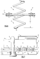
- interconnector 15 includes a dielectric member 17 adapted for being positioned between first and second electrical circuit members 19 and 21 (FIG. 7).
- member 19 is illustrated as a module and thus includes a substrate 23 with a plurality of conductors 25 along a bottom surface 27 thereof.
- Each conductor is preferably a metallic (e.g., copper) pad of relatively flat construction but may assume other configurations as are known in the art. It is desirable to overplate conductors (25) with nickel and gold to prevent corrosion and also provide a highly reliable connection for the present invention.
- Circuit member 19 may also include a plurality of semiconductor chips 29 (only one shown in FIG. 7), which in turn are electrically coupled to pads 25 through internal circuitry (not shown) within substrate 23.
- An additional cover 31 or the like may be provided on the substrate's upper surface 33.
- a typical substrate material for circuit member 19 is ceramic, but others are of course acceptable.
- the lower circuit member 21 is shown as a printed circuit board and also includes a substrate portion 35, which may be comprised of known material (e.g., epoxy resin reinforced with fiberglass) and, as stated above, may include pluralities of conductive planes (e.g., signal, power or ground) internally thereof.
- a substrate portion 35 which may be comprised of known material (e.g., epoxy resin reinforced with fiberglass) and, as stated above, may include pluralities of conductive planes (e.g., signal, power or ground) internally thereof.
- conductive planes e.g., signal, power or ground
- Conductors 37 are similar (e.g., copper) to conductors 25 and also preferably include nickel and gold overplate for the reasons stated above.
- dielectric member 17 is positioned substantially between both circuit members 19 and 21 in a predetermined manner of alignment.
- alignment may be accomplished using a plurality of alignment pins 41 (only one shown in FIG. 7), each pin fitting within respective apertures 43 and 45 located within circuit members 21 and 19, respectively.
- Alignment with dielectric member 17 is accomplished by providing an opening 47 within the dielectric and passing one of the pins 41 therethrough.
- a total of two pins 41 are utilized, each at respective opposite corners of the overall rectangular shaped structure. This is not meant to limit the invention, however, in that additional numbers of such pins may be utilized.
- dielectric member 17 is shown to include upper and lower layers 51 and 53.
- Each layer is preferably comprised of a polymer material, a preferred such material being polyimide, this material laminated onto the outer surfaces of an interim electrically conductive element 55 which represents the electrically conducting portion of interconnector 15.
- Each polyimide layer 51 and 53 preferably possesses a thickness of from about .001 inch to about .003 inch. Although only one such conductive element is shown in FIG. 6, it is understood that several such elements may be utilized in the invention, depending on the operational requirements for the final assembly which will utilize the present invention. In one example, a total of 625 such elements 55 may be used.
- Conductive element 55 includes a relatively flat base portion 59 which, as shown in FIG. 6, is located substantially between the outer, surrounding layers 51 and 53. Alternatively, it is within the scope of the invention that this conductive, relatively flat base portion 59 be located externally of a singular dielectric layer, also preferably of polyimide, to thus present only a dual layered structure for this portion of the invention. Additionally, conductive element 55 includes at least one resilient helical portion 61 which extends in a direction away from the flat base portion 59. In the embodiment of FIG. 6, two helical portions are shown, each extending in opposite directions (up and down) from the interim, relatively flat base portion 55. Each helical portion, as understood, is designed for engaging a respective electrical conductor 25 or 37. In the embodiment of FIG.
- interconnector 15 provides an electrical connection between a first conductor 25 and an associated second conductor 37.
- FIG. 6 Although two opposing helical portions 61 are shown in the embodiment in FIG. 6, it is understood that alternative embodiments are well within the scope of the invention. For example, it is possible, as defined herein, to utilize but a singular helical portion and provide alternative means for coupling to the other conductor. Such an embodiment is depicted in FIGS. 9 and 11 and will be described in further detail hereinbelow. Significantly, it is also possible to provide two helical portions on one side of the interconnector, to thus assure redundancy of connection. Such a feature is considered particularly significant and desirable.
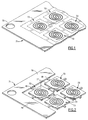
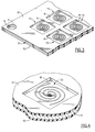
- FIGS. 1-5 there are shown the various steps of producing interconnector 15 in accordance with a preferred embodiment of the invention.
- a singular sheet 71 of flat conductive material is provided.
- a preferred conductive material for this sheet, which sheet will eventually form the conductive element of the invention, is beryllium copper.
- Other metallic materials are acceptable, including phospor-bronze.
- a sheet 71 having a thickness of about .005 inch was used, with side dimensions of about 1.5 inch by about 1.5 inch.
- a total of 625 conductive elements may be formed in a sheet of this size, indicating the extremely high density capabilities of the invention.
- a grouping of predetermined-shaped curvilinear elements 73 and rectangular "pads" 77 are formed in FIG. 1, preferably using an etching procedure or the like. Such a procedure may be of one known in the art and further description is not believed necessary.
- Each of these formed, curved elements is understood to eventually comprise the expanded helical portions of the respective conductive elements 55 of the invention as shown in FIG. 6.
- an opening 75 is also preferably provided as shown, such opening to eventually be adapted for receiving one of the alignment pins 41 (FIG. 7).
- the pattern necessary to enable etching of the curvilinear elements and pads shown in FIG. 1 is preferably provided using known photolithography steps as may be used in many printed circuit board manufacturing operations. Accordingly, further description is not believed necessary.
- FIG. 2 shows the curved elements 73 and pads 77 formed.
- Each of the helical elements 73 remains formed within a substantially rectangular pad 77, each pad 77 connected to an adjacent such pad or to the surrounding boundary (peripheral) portion 79 of sheet 71 through a connecting tab 81.
- Each pad 71 is thus connected on each of its four sides by one of these tabs.
- each tab may possess a width of only about .005 to .010 inch.
- etching has been defined as the preferred means for material removal from sheet 71, alternative means are within the scope of the invention, including laser ablation and stamping.
- sheet 71 of the same configuration as in FIG. 2, is now substantially covered on opposite surfaces thereof with a layer of dielectric material 51 and 53 (described above).
- this dielectric is applied using lamination techniques, several of which are known in the art, and further description is not believed necessary.
- a window 91 is provided within each layer relative to one of the elements 73. This window, preferably rectangular, is slightly less than the corresponding width of the rectangular pad sections 77. This slight overlap can be seen in the cross-sectional view of FIG. 6.
- Each layer 51 and 53 is of the thickness described above in FIG. 6.
- Each window 91 is preferably square and possesses side dimensions each of about .035 inch, in comparison to the respective side dimensions for its pad 77, which dimensions are preferably slightly larger at .045 inch square.
- the overall thickness for this structure of FIG. 3, including that of the two dielectric layers and interim metallic sheet 71, is thus about .010 inch.
- the dielectric is also provided with the aforementioned opening 47 therein which, as shown, aligns with the respective opening 75 in sheet 71.
- the next step in the manufacture of the invention involves the provision of a plurality of dendritic elements 93 on the curved, terminal ends of the curvilinear segments 73.
- these elements 93 are shown only on one of these curved ends and project upwardly in this perspective view. Should this particular segment eventually form a dual, opposed projecting conductive element as shown in FIG. 6, the underside of the other, adjacent curved terminal end would be similarly provided with such dendritic elements.
- Dendritic formation is preferably accomplished in accordance with the techniques defined in Canadian Patent 1,121,011, the disclosure of which is incorporated herein by reference. This is not meant to limit the invention, however, in that other techniques for applying such elements may be utilized.
- these elements may be comprised of a conductive material selected from the group consisting essentially of palladium, platinum, rhodium, ruthenium, osmium, iridium and tungsten.
- a conductive material selected from the group consisting essentially of palladium, platinum, rhodium, ruthenium, osmium, iridium and tungsten.
- Such elements are grown on the metallic (beryllium copper) substrate and may be done so in the presence of the surrounding polyimide dielectric material which forms layers 51 and 53 without adversely affecting such layers.
- Use of dendritic elements constitutes an important aspect of the invention for the several advantages described for these elements mentioned in the aforementioned patent. For example, such elements are especially effective in debris removal from respective surfaces to which these engage.
- the conductive element of the invention is capable of engaging flat surfaces (e.g., copper pads) and also may engage conductors having dendritic or similar elements of the type described herein.
- the dendritic elements 93 provide sound, effective connection. Of further significance, such connection is in a non-wiping form of engagement, due to the shape of the helical part of the invention's conductive element and its compressibility when engaged.
- Dendritic elements 93 are also shown in the embodiments of FIGS. 8-11. In one example of the invention, a total of approximately 1000 dendritic elements 93 may be formed on each curved terminal end.
- each of the substantially rectangular shaped segments 77 is electrically isolated from adjacent segments and also from the boundary (peripheral) portions 79 of the interim sheet 71.
- This is preferably accomplished by punching or laser ablation wherein apertures 95 are formed within the composite structure.
- Each aperture understandably, extends through the entire thickness of this composite structure.
- this punching or similar removal operation causes a separation of the connecting tabs 81 to thereby isolate the previously formed pad sections so as to form the now finally identified conductive elements 55 of the configuration depicted in the cross-sectional view in FIG. 6 prior to helical extension.
- each helical portion of the invention is extended outwardly a predetermined distance.
- Such extension is preferably accomplished by a die forming operation, whereby each helical portion is formed to the desired dimensions.
- each helical portion extends a distance (dimension "D") of about .020 inch from the respective outer surface of the adjacent dielectric layer. This is not meant to limit the invention, however, in that other extensions may be provided, depending on the corresponding dimensional constraints of the structure receiving the invention.
- the beryllium copper outer surfaces Prior to formation of the defined dendritic elements 93, it is also preferred to plate the beryllium copper outer surfaces with a layer of nickel and thereafter provide an extremely thin coating of precious metal (e.g., gold), the nickel serving as a diffusion barrier.
- the defined dendritic elements are then formed (e.g., grown) on this metallic substrate.
- a nickel layer having a thickness of about 60-80 microinches and a gold layer having a thickness of about 50-100 microinches was formed.
- FIGS. 8-11 there are shown alternate embodiments of the invention.
- interconnector 15 includes dual helical portions 61 but each of these portions are extended from the conductive element's base portion 59 in a singular, common direction (downward in FIG. 8). This is accomplished by merely depressing both helical portions shown, for example, in the embodiment of FIG. 5, downwardly.
- the advantage of this structure is that it assures redundancy of connection with the respective conductor 37 to which it engages.
- Each terminal end of these helical portions includes, preferably, the described dendritic elements 93.
- means 97 for providing electrical connection between base portion 59 and the remaining conductor 25.
- this means is preferably a plurality of dendritic elements 93' formed on the opposite surface of the base portion 59 in accordance with similar teachings for the formation of elements 93. Such dendritic formation may occur simultaneously with the formation of elements 93. Dendritic elements 93' engage conductor 25 during compression of interconnector 15, as caused by bringing together circuit members 19 and 21. Such compression of the circuit members may be accomplished using various means in the art (e.g., external clamping structures), and further description is not believed necessary.
- interconnector 15 includes but a singular helical portion 61 projecting downwardly with the other formed helical portion remaining coplanar with base portion 59. This additional surface area enables the provision of additional dendritic elements 93', which dendritic elements 93' form the means of electrical connection to conductor 25.
- each of the invention's helical portions may be compressed a distance of about .020 inch from its overall initial height (dimension "D") in Fig. 6.
- interconnector 15 includes the dual helical portions 61 of similar configuration to those in FIG. 8.
- means 97 preferably comprises a quantity of solder 99.
- solder 99 was 63:37 tin:lead, wherein the tin comprised about 63% of the solder composition with the lead comprising the remaining 37%.
- Alternative solders are of course acceptable, including 90:10 tin:lead, wherein the tin comprises about 90% with the remaining 10% comprised of lead. This provides a fixed type of connection between the conductive element of the invention and one of the respective conductors being coupled.
- solder material 99 preferably similar to that in the embodiment of FIG. 10, is utilized to form the relatively fixed connection between conductor 25 and conductive element 55.
- solder material 99 preferably similar to that in the embodiment of FIG. 10 is utilized to form the relatively fixed connection between conductor 25 and conductive element 55.
- Use of a singular helical portion, as in the embodiment of FIG. 9, allows for greater surface area for receiving the preferred solder.
- an electrical interconnector for interconnecting a pair of circuit members wherein the interconnector is designed for being positioned between the two circuit members.
- the invention is able to accommodate for non-planarity of the respective circuit members and/or the conductors thereon while still assuring effective coupling therebetween.
- the invention as defined is relatively simple to produce and relatively easy to operate.
- the invention has been described as a means for providing electrical connection between respective pairs of conductors, it is also possible to utilize the metallic conductor for heat transference (e.g., from module to board) should this be desired. Accordingly, it is possible to utilize a plurality of such heat transferring members in combination with the interconnecting structure defined herein to thus assure both thermal and electrical paths at designated locations within a combined structure.
Landscapes
- Engineering & Computer Science (AREA)
- Microelectronics & Electronic Packaging (AREA)
- Coupling Device And Connection With Printed Circuit (AREA)
Applications Claiming Priority (2)
| Application Number | Priority Date | Filing Date | Title |
|---|---|---|---|
| US959839 | 1992-10-13 | ||
| US07/959,839 US5297967A (en) | 1992-10-13 | 1992-10-13 | Electrical interconnector with helical contacting portion and assembly using same |
Publications (2)
| Publication Number | Publication Date |
|---|---|
| EP0592844A2 true EP0592844A2 (fr) | 1994-04-20 |
| EP0592844A3 EP0592844A3 (en) | 1995-12-13 |
Family
ID=25502479
Family Applications (1)
| Application Number | Title | Priority Date | Filing Date |
|---|---|---|---|
| EP93115167A Withdrawn EP0592844A3 (en) | 1992-10-13 | 1993-09-21 | Electrical interconnector with helical contacting portion and assembly using same |
Country Status (3)
| Country | Link |
|---|---|
| US (1) | US5297967A (fr) |
| EP (1) | EP0592844A3 (fr) |
| JP (1) | JP2620502B2 (fr) |
Cited By (1)
| Publication number | Priority date | Publication date | Assignee | Title |
|---|---|---|---|---|
| EP0996197A3 (fr) * | 1998-10-23 | 2003-01-29 | Nokia Corporation | Dispositif de connexion électrique et instrument électronique utilisant ce dispostif |
Families Citing this family (55)
| Publication number | Priority date | Publication date | Assignee | Title |
|---|---|---|---|---|
| US5476211A (en) * | 1993-11-16 | 1995-12-19 | Form Factor, Inc. | Method of manufacturing electrical contacts, using a sacrificial member |
| US6191368B1 (en) * | 1995-09-12 | 2001-02-20 | Tessera, Inc. | Flexible, releasable strip leads |
| US5604445A (en) * | 1994-12-21 | 1997-02-18 | International Business Machines Corporation | Apparatus, and corresponding method, for stress testing semiconductor chips |
| JP3653131B2 (ja) * | 1995-12-28 | 2005-05-25 | 日本発条株式会社 | 導電性接触子 |
| US5949246A (en) * | 1997-01-28 | 1999-09-07 | International Business Machines | Test head for applying signals in a burn-in test of an integrated circuit |
| US6224396B1 (en) | 1997-07-23 | 2001-05-01 | International Business Machines Corporation | Compliant, surface-mountable interposer |
| US6441315B1 (en) * | 1998-11-10 | 2002-08-27 | Formfactor, Inc. | Contact structures with blades having a wiping motion |
| US6717421B1 (en) * | 1999-09-09 | 2004-04-06 | Nhk Spring Co., Ltd. | Electric contact probe assembly |
| US6474997B1 (en) * | 1999-09-30 | 2002-11-05 | Ngk Insulators, Ltd. | Contact sheet |
| US6434817B1 (en) | 1999-12-03 | 2002-08-20 | Delphi Technologies, Inc. | Method for joining an integrated circuit |
| US6464513B1 (en) | 2000-01-05 | 2002-10-15 | Micron Technology, Inc. | Adapter for non-permanently connecting integrated circuit devices to multi-chip modules and method of using same |
| DE10014338C1 (de) * | 2000-03-24 | 2001-10-04 | Heraeus Gmbh W C | Andruckverbinder |
| US7045889B2 (en) * | 2001-08-21 | 2006-05-16 | Micron Technology, Inc. | Device for establishing non-permanent electrical connection between an integrated circuit device lead element and a substrate |
| US7049693B2 (en) * | 2001-08-29 | 2006-05-23 | Micron Technology, Inc. | Electrical contact array for substrate assemblies |
| JP3703748B2 (ja) * | 2001-09-05 | 2005-10-05 | 山一電機株式会社 | Icソケット |
| US7275562B2 (en) * | 2001-10-17 | 2007-10-02 | Agilent Technologies, Inc. | Extensible spiral for flex circuit |
| US7265565B2 (en) | 2003-02-04 | 2007-09-04 | Microfabrica Inc. | Cantilever microprobes for contacting electronic components and methods for making such probes |
| US20050104609A1 (en) * | 2003-02-04 | 2005-05-19 | Microfabrica Inc. | Microprobe tips and methods for making |
| US20050184748A1 (en) * | 2003-02-04 | 2005-08-25 | Microfabrica Inc. | Pin-type probes for contacting electronic circuits and methods for making such probes |
| US9533376B2 (en) | 2013-01-15 | 2017-01-03 | Microfabrica Inc. | Methods of forming parts using laser machining |
| US20060006888A1 (en) * | 2003-02-04 | 2006-01-12 | Microfabrica Inc. | Electrochemically fabricated microprobes |
| JP3814231B2 (ja) * | 2002-06-10 | 2006-08-23 | 株式会社アドバンストシステムズジャパン | スパイラルコンタクタ及びその製造方法、並びにそれを用いた半導体検査装置、及び電子部品 |
| JP4213559B2 (ja) * | 2002-12-27 | 2009-01-21 | 日本碍子株式会社 | コンタクトシート及びその製造方法並びにソケット |
| US20080157793A1 (en) * | 2003-02-04 | 2008-07-03 | Microfabrica Inc. | Vertical Microprobes for Contacting Electronic Components and Method for Making Such Probes |
| US10416192B2 (en) | 2003-02-04 | 2019-09-17 | Microfabrica Inc. | Cantilever microprobes for contacting electronic components |
| US20080211524A1 (en) * | 2003-02-04 | 2008-09-04 | Microfabrica Inc. | Electrochemically Fabricated Microprobes |
| JP3924542B2 (ja) * | 2003-02-07 | 2007-06-06 | アルプス電気株式会社 | 電子コネクタ |
| TW573844U (en) * | 2003-06-13 | 2004-01-21 | Hon Hai Prec Ind Co Ltd | Electrical connector contact |
| JP3795898B2 (ja) * | 2003-06-20 | 2006-07-12 | アルプス電気株式会社 | 接続装置 |
| US7422446B2 (en) * | 2003-08-01 | 2008-09-09 | Alps Electric Co., Ltd. | Connector |
| JP4079857B2 (ja) * | 2003-09-09 | 2008-04-23 | アルプス電気株式会社 | 接続装置の製造方法 |
| JP2005156522A (ja) * | 2003-10-27 | 2005-06-16 | Sumitomo Electric Ind Ltd | コンタクトの製造方法とその方法により製造されたコンタクト |
| JP2005129428A (ja) * | 2003-10-27 | 2005-05-19 | Sumitomo Electric Ind Ltd | 竹の子状コンタクトの製造方法、その方法により製造されたコンタクトおよびそのコンタクトを備える検査装置または電子機器 |
| US7185430B2 (en) * | 2003-11-28 | 2007-03-06 | Ngk Insulators, Ltd. | Method of manufacturing contact sheets |
| KR20050059417A (ko) * | 2003-12-12 | 2005-06-20 | 스미토모덴키고교가부시키가이샤 | 소용돌이 단자와 그 제조방법 |
| TW200535425A (en) * | 2003-12-31 | 2005-11-01 | Microfabrica Inc | Pin-type probes for contacting electronic circuits and methods for making such probes |
| JP2005251487A (ja) * | 2004-03-03 | 2005-09-15 | Alps Electric Co Ltd | スパイラル接触子及びスパイラルシート並びにスパイラル接触子の製造方法 |
| JP4068610B2 (ja) * | 2004-10-01 | 2008-03-26 | 山一電機株式会社 | 半導体装置用キャリアユニットおよびそれを備える半導体装置用ソケット |
| US7515951B2 (en) * | 2005-06-23 | 2009-04-07 | International Business Machines Corporation | Assembly, system, and method for optimizing image quality |
| JP4549246B2 (ja) * | 2005-07-08 | 2010-09-22 | モレックス インコーポレイテド | ソケット |
| ATE452418T1 (de) * | 2006-09-12 | 2010-01-15 | Koninkl Philips Electronics Nv | Leuchte mit einem in die quarzglashülle der leuchte integrierten leiter |
| US7568917B1 (en) * | 2008-01-10 | 2009-08-04 | Tyco Electronics Corporation | Laminated electrical contact strip |
| US7914294B2 (en) | 2008-07-16 | 2011-03-29 | GM Global Technology Operations LLC | Flexible electric bus bar in a small space |
| JP4775976B2 (ja) * | 2009-03-09 | 2011-09-21 | 株式会社アドバンストシステムズジャパン | シート状接続端子およびこれを使用したfpc基板の接続方法 |
| JP5386277B2 (ja) * | 2009-09-03 | 2014-01-15 | 新光電気工業株式会社 | 巻形状ばね部材、半導体パッケージ用ソケット及び製造方法 |
| US8959764B2 (en) * | 2009-11-06 | 2015-02-24 | International Business Machines Corporation | Metallurgical clamshell methods for micro land grid array fabrication |
| US8263879B2 (en) * | 2009-11-06 | 2012-09-11 | International Business Machines Corporation | Axiocentric scrubbing land grid array contacts and methods for fabrication |
| US8133061B1 (en) * | 2010-11-29 | 2012-03-13 | International Business Machines Corporation | Removable and replaceable dual-sided connector pin interposer |
| JP6406645B2 (ja) * | 2015-12-10 | 2018-10-17 | アルプス電気株式会社 | 圧接コネクタ |
| US20170279104A1 (en) * | 2016-03-22 | 2017-09-28 | Faraday&Future Inc. | Flexible circuit for vehicle battery |
| TWI649923B (zh) * | 2016-06-17 | 2019-02-01 | 日商阿爾普士電氣股份有限公司 | Crimp type joint and manufacturing method thereof |
| US11262383B1 (en) | 2018-09-26 | 2022-03-01 | Microfabrica Inc. | Probes having improved mechanical and/or electrical properties for making contact between electronic circuit elements and methods for making |
| TWI700025B (zh) * | 2018-10-04 | 2020-07-21 | 群光電子股份有限公司 | 多層電路板結構 |
| US11189563B2 (en) * | 2019-08-01 | 2021-11-30 | Nanya Technology Corporation | Semiconductor structure and manufacturing method thereof |
| US11935860B2 (en) * | 2020-03-24 | 2024-03-19 | Intel Corporation | Electrical connector with insulated conductive layer |
Family Cites Families (17)
| Publication number | Priority date | Publication date | Assignee | Title |
|---|---|---|---|---|
| NL7003475A (fr) * | 1969-03-28 | 1970-09-30 | ||
| US4027935A (en) * | 1976-06-21 | 1977-06-07 | International Business Machines Corporation | Contact for an electrical contactor assembly |
| IT1112620B (it) * | 1977-04-15 | 1986-01-20 | Ibm | Connettore elettrico perfezionato |
| US4705205A (en) * | 1983-06-30 | 1987-11-10 | Raychem Corporation | Chip carrier mounting device |
| US4620761A (en) * | 1985-01-30 | 1986-11-04 | Texas Instruments Incorporated | High density chip socket |
| US4793814A (en) * | 1986-07-21 | 1988-12-27 | Rogers Corporation | Electrical circuit board interconnect |
| US5137461A (en) * | 1988-06-21 | 1992-08-11 | International Business Machines Corporation | Separable electrical connection technology |
| FR2639154B1 (fr) * | 1988-11-15 | 1990-12-21 | Thomson Csf | Connecteur de transformation d'un boitier specifique de circuit integre a plots de connexion en un boitier standard a broches de connexion |
| US4961709A (en) * | 1989-02-13 | 1990-10-09 | Burndy Corporation | Vertical action contact spring |
| US4927369A (en) * | 1989-02-22 | 1990-05-22 | Amp Incorporated | Electrical connector for high density usage |
| EP0385142B1 (fr) * | 1989-02-28 | 1995-09-27 | Fujitsu Limited | Dispositif de connexion électrique |
| US4922376A (en) * | 1989-04-10 | 1990-05-01 | Unistructure, Inc. | Spring grid array interconnection for active microelectronic elements |
| US5037311A (en) * | 1989-05-05 | 1991-08-06 | International Business Machines Corporation | High density interconnect strip |
| DE4018206A1 (de) * | 1990-06-07 | 1991-12-12 | Vdo Schindling | Elektrische kontaktvorrichtung |
| US5030109A (en) * | 1990-08-24 | 1991-07-09 | Amp Incorporated | Area array connector for substrates |
| DE69131136T2 (de) * | 1990-10-29 | 1999-12-09 | General Datacomm, Inc. | Elektrischer verbinder mit konischem federkontaktelement |
| US5061191A (en) * | 1990-12-21 | 1991-10-29 | Amp Incorporated | Canted coil spring interposing connector |
-
1992
- 1992-10-13 US US07/959,839 patent/US5297967A/en not_active Expired - Fee Related
-
1993
- 1993-09-21 EP EP93115167A patent/EP0592844A3/en not_active Withdrawn
- 1993-10-04 JP JP5248272A patent/JP2620502B2/ja not_active Expired - Lifetime
Cited By (1)
| Publication number | Priority date | Publication date | Assignee | Title |
|---|---|---|---|---|
| EP0996197A3 (fr) * | 1998-10-23 | 2003-01-29 | Nokia Corporation | Dispositif de connexion électrique et instrument électronique utilisant ce dispostif |
Also Published As
| Publication number | Publication date |
|---|---|
| JP2620502B2 (ja) | 1997-06-18 |
| EP0592844A3 (en) | 1995-12-13 |
| JPH06203933A (ja) | 1994-07-22 |
| US5297967A (en) | 1994-03-29 |
Similar Documents
| Publication | Publication Date | Title |
|---|---|---|
| US5297967A (en) | Electrical interconnector with helical contacting portion and assembly using same | |
| EP0491269B1 (fr) | Connecteur à haute densité | |
| US5163834A (en) | High density connector | |
| US5759047A (en) | Flexible circuitized interposer with apertured member and method for making same | |
| EP0574715B1 (fr) | Méthode de formation d'une partie terminale conductrice d'un circuit flexible | |
| US5248262A (en) | High density connector | |
| US5953214A (en) | Dual substrate package assembly coupled to a conducting member | |
| US5137456A (en) | High density, separable connector and contact for use therein | |
| US6545226B2 (en) | Printed wiring board interposer sub-assembly | |
| EP0159593B1 (fr) | Connecteur électrique et méthode pour fabriquer celui-ci | |
| US6224396B1 (en) | Compliant, surface-mountable interposer | |
| JP4584144B2 (ja) | 回路基板装置及び配線基板間接続方法 | |
| US4295184A (en) | Circuit board with self-locking terminals | |
| JP2738498B2 (ja) | 支持された突出した構造の電気相互接続 | |
| JPH05226043A (ja) | 電気的接触体及び電気的コネクタアツセンブリ | |
| KR101334795B1 (ko) | 전기신호 접속용 좌표 변환장치 | |
| US20120138343A1 (en) | Three dimensional interposer device, chip package and probe card contactor | |
| US6723927B1 (en) | High-reliability interposer for low cost and high reliability applications | |
| US7293995B2 (en) | Electrical contact and connector system | |
| US6641406B1 (en) | Flexible connector for high density circuit applications | |
| US4223435A (en) | Circuit board with self-locking terminals | |
| EP0792519B1 (fr) | Elements d'interconnexion pour composants micro-electroniques | |
| KR20250021064A (ko) | 2개의 회로 요소를 접속하기 위한 단일편 수직력 전기 커넥터 | |
| JPH10125369A (ja) | 電子部品の接続方法及び接続構造 | |
| JPH11102742A (ja) | コネクタ又はプローブの構造 |
Legal Events
| Date | Code | Title | Description |
|---|---|---|---|
| PUAI | Public reference made under article 153(3) epc to a published international application that has entered the european phase |
Free format text: ORIGINAL CODE: 0009012 |
|
| AK | Designated contracting states |
Kind code of ref document: A2 Designated state(s): DE FR GB |
|
| 17P | Request for examination filed |
Effective date: 19940819 |
|
| PUAL | Search report despatched |
Free format text: ORIGINAL CODE: 0009013 |
|
| AK | Designated contracting states |
Kind code of ref document: A3 Designated state(s): DE FR GB |
|
| 18W | Application withdrawn |
Withdrawal date: 19960923 |