EP0592899B1 - Microscope électronique à balayage - Google Patents
Microscope électronique à balayage Download PDFInfo
- Publication number
- EP0592899B1 EP0592899B1 EP93115912A EP93115912A EP0592899B1 EP 0592899 B1 EP0592899 B1 EP 0592899B1 EP 93115912 A EP93115912 A EP 93115912A EP 93115912 A EP93115912 A EP 93115912A EP 0592899 B1 EP0592899 B1 EP 0592899B1
- Authority
- EP
- European Patent Office
- Prior art keywords
- electrode
- electron beam
- electric field
- specimen
- secondary electrons
- Prior art date
- Legal status (The legal status is an assumption and is not a legal conclusion. Google has not performed a legal analysis and makes no representation as to the accuracy of the status listed.)
- Expired - Lifetime
Links
- 238000010894 electron beam technology Methods 0.000 claims description 63
- 230000005684 electric field Effects 0.000 claims description 52
- 230000003287 optical effect Effects 0.000 claims description 13
- 230000000694 effects Effects 0.000 claims description 10
- 238000001816 cooling Methods 0.000 claims 2
- 238000000034 method Methods 0.000 description 9
- 230000005284 excitation Effects 0.000 description 7
- 201000009310 astigmatism Diseases 0.000 description 6
- 238000010586 diagram Methods 0.000 description 4
- 230000004075 alteration Effects 0.000 description 3
- 230000006399 behavior Effects 0.000 description 3
- 239000002131 composite material Substances 0.000 description 3
- IJGRMHOSHXDMSA-UHFFFAOYSA-N Atomic nitrogen Chemical compound N#N IJGRMHOSHXDMSA-UHFFFAOYSA-N 0.000 description 2
- 230000001133 acceleration Effects 0.000 description 2
- 230000002411 adverse Effects 0.000 description 2
- 238000001514 detection method Methods 0.000 description 2
- 230000005672 electromagnetic field Effects 0.000 description 2
- 238000005452 bending Methods 0.000 description 1
- 238000010276 construction Methods 0.000 description 1
- 238000011109 contamination Methods 0.000 description 1
- 239000006185 dispersion Substances 0.000 description 1
- 230000003993 interaction Effects 0.000 description 1
- 230000001678 irradiating effect Effects 0.000 description 1
- 239000007788 liquid Substances 0.000 description 1
- 229910052757 nitrogen Inorganic materials 0.000 description 1
- 238000004626 scanning electron microscopy Methods 0.000 description 1
Images



Classifications
-
- H—ELECTRICITY
- H01—ELECTRIC ELEMENTS
- H01J—ELECTRIC DISCHARGE TUBES OR DISCHARGE LAMPS
- H01J37/00—Discharge tubes with provision for introducing objects or material to be exposed to the discharge, e.g. for the purpose of examination or processing thereof
- H01J37/02—Details
- H01J37/244—Detectors; Associated components or circuits therefor
-
- H—ELECTRICITY
- H01—ELECTRIC ELEMENTS
- H01J—ELECTRIC DISCHARGE TUBES OR DISCHARGE LAMPS
- H01J2237/00—Discharge tubes exposing object to beam, e.g. for analysis treatment, etching, imaging
- H01J2237/244—Detection characterized by the detecting means
- H01J2237/2443—Scintillation detectors
-
- H—ELECTRICITY
- H01—ELECTRIC ELEMENTS
- H01J—ELECTRIC DISCHARGE TUBES OR DISCHARGE LAMPS
- H01J2237/00—Discharge tubes exposing object to beam, e.g. for analysis treatment, etching, imaging
- H01J2237/26—Electron or ion microscopes
- H01J2237/28—Scanning microscopes
Definitions
- the present invention relates to a scanning electron microscope that obtains a scan image on the basis of secondary electrons emitted by irradiating an electron beam to a specimen. More particularly, it concerns a scanning electron microscope that is capable of efficiently capturing secondary electrons to obtain an image of high resolution.
- a most popular method for improving resolution of a scanning electron microscope is to shorten a focal length of an object lens with a specimen placed in a magnetic field of the objective lens.
- Methods of placing the specimen in the magnetic field of the objective lens include a so-called in-lens method that places the specimen between magnetic poles of the objective lens, as disclosed in, for example, the Japanese Patent Application Laid-Open No. 63-110543, and a method that an objective lens (snorkel lens) is shaped to allow an objective lens magnetic field to leak out to a specimen side so that the specimen is substantially placed in the objective lens magnetic field even if the specimen is put below the objective lens, as disclosed by Mulvey in "Scanning Electron Microscopy," 1974, p44.
- the secondary electrons emitted from the specimen are captured by the magnetic field of the object lens to travel to a top of the objective lens. For this reason, the secondary electrons emitted from the specimen must be detected at the top of the objective lens.
- the specimen is preferably placed as close to a bottom of the objective lens.
- the secondary electrons have to be detected at a top of the objective lens.
- the secondary electron detector In order that the secondary electron detector captures the secondary electrons, the secondary electron detector has a high voltage of around 10 kV applied thereto to produce an attracting electric field.
- the attracting electric field undesirably bends an orbit of the primary electron beam.
- the bent orbit changes an incoming position of the primary electron beam on the object lens, causing an axial deviation.
- the attracting electric field produced by the secondary electron detector causes astigmatism and other disturbances in itself. These difficulties are too high to realize high resolution.
- the Japanese Patent Application Laid-Open No. 52-91361 has a shielding casing for covering an electron beam path in front of a secondary electron detector.
- the shielding casing cannot fully prevent the effect of the electric field of the secondary electron detector as the secondary electrons cannot be detected unless the electric field leaks onto the optical axis.
- the Japanese Patent Application Laid-Open No. 63-110543 has the attracting electric field produced by the secondary electron detector formed axially symmetrical.
- this involves a problem that the detection efficiency of the secondary electrons around the center axis is lowered because of the axial symmetry of the attracting electric field of the secondary electrons.
- the Japanese Utility model Application Laid-Open No. 61-99960 shows a method that an orbit of the primary electron beam bent by an attracting electric field of a secondary electron detector is corrected by a two-stage deflector provided at a top of the secondary electron detector.
- this method cannot prevent the attracting electric field produced by the secondary electron detector from leaking into an electron beam path, causing adverse effects, such as astigmatism.
- the Japanese Patent Application Laid Open No. 60-212953 discloses a method that additional electrodes and coils are provided to make the electric field and magnetic field orthogonal to correct a bent orbit of the primary electron beam before leading secondary electrons to a secondary electron detector positioned above the electrodes and coils.
- this method does not take into account any of leaking of a non-uniform attracting electric field produced by the secondary electron detector onto the optical axis.
- each of the prior arts has its merits and demerits. It has been demanded to have a scanning electron microscope capable of detecting secondary electrons further efficiently.
- an object of the present invention to provide a scanning electron microscope capable of efficiently detecting secondary electrons without astigmatism and axial deviation even with detection of the secondary electrons above an objective lens.
- the shielding electrode can shield the attracting electric field produced by the secondary electron detector to capture the secondary electrons, thereby preventing the attracting electric field from leaking into the electron beam path.
- the magnetic field produced by the coils can correct the orbit of the primary electron beam bend by action of the deflecting electric field produced by the shielding electrode, thereby preventing the primary electron beam from deviating axially.
- the secondary electrons these can be easily detected as the deflection direction of the magnetic field is made the same as that of the deflecting electric field to make deflection of the secondary electrons large.
- Fig. 1 depicts a cross-sectional view illustrating a secondary electron detector 50 and its peripheries of a scanning electron microscope according to the present invention.
- An electron source emits a primary electron beam 4.
- the primary electron beam is irradiated depthwise from outside to inside in the drawing.
- a secondary electron detector 50 comprises an attracting electrode 51, a scintillator 52, and light guide 53. Secondary electrons are attracted by an attracting electric field 54 generated by the attracting electrode 51 and are accelerated to the scintillator 52 by a positive potential applied thereto to thereby radiate light from the scintillator 52. The radiated light is guided by the light guide 53 to a photomultiplier (not shown) to be converted into an electric signal, which is fed to an intensity modulation input of a CRT.
- a shielding electrode 12 is provided between the secondary electron detector 50 and the electron beam path to cover parts of an electron beam path.
- An opposed electrode 11 is also provided at a position facing the shielding electrode 12 to put the electron beam path there between.
- the shielding electrode 12 can be a porous plate or mesh-like member having a transparency for the secondary electron and having a shielding effect for the attracting electric field 54.
- a potential difference V is applied between the shielding electrode 12 and the opposed electrode 11 to produce a deflection electric field E.
- two sets of optical axis correction coils 19 and 20 are provided around the electron beam path and are supplied with excitation currents so as to produce a composite or combined excitation current I(A) to generate a corresponding composite or combined magnetic field B in the electron beam path in a direction orthogonal to the deflecting electric field E and the electron beam optical path.
- Kb is a constant determined in terms of shapes and positions of the optical axis correction coils 19 and 20.
- the primary electron beam 4 can be made to go straightly forward without any action.
- the deflecting electric field E and the magnetic field B are virtually uniform around the optic axis, there will not occur an astigmatism due to non-uniform electromagnetic distribution.
- the deflecting electric field E can deflect the secondary electrons 9 emitted from a specimen 7 in the same direction as the primary electron beam 4.
- the magnetic field B as shown in Fig. 4, can deflect the secondary electrons 9 in the direction reverse to the primary electron beam 4 since the secondary electrons 9 go opposite to the primary electron beam 4.
- both the deflecting electric field E and the magnetic field B make action to the secondary electrons 9 to lead the same to the secondary electron detector 50, they sharply bend the orbit of the secondary electrons 9 having little energy to transmit through the shielding electrode 12 so that the secondary electrons 9 are captured by the secondary electron detector 50.
- the non-uniform attracting electric field 54 produced from the secondary electron detector 50 is shielded by the shielding electrode 12, the attracting electric field 54 cannot affect the primary electron beam 4, causing no astigmatism.
- Wien filter Means making the deflecting electric field E and the magnetic field B orthogonal to each other has been known as a kind of energy filter called the Wien filter.
- the electromagnetic field strength needed for the energy filter causes the electron beam to disperse the energy, resulting in a large chromatic aberration.
- the electromagnetic field strength for bending the orbit of the secondary electron having a few to some ten electron volts causes so little energy dispersion in the primary electron beam having tens of times the energy that the effect to the chromatic aberration can be virtually ignored.
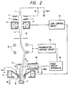
- Fig. 2 depicts a schematic diagram illustrating a scanning electron microscope of the embodiment of the present invention. Arrangements and parts in the Figure identical with those mentioned above are indicated by the same numbers as above.
- the primary electron beam 4 is radiated from a cathode 1 by an extracting voltage V1 applied between the cathode 1 and a first anode 2.
- the primary electron beam 4 then is accelerated by the accelerating voltage Vacc applied between the cathode 1 and a second anode 3 to travel to a succeeding lens system.
- the accelerated primary electron beam 4 is focused into a minute spot on the specimen 7 by the lens action of a focusing lens 5 and an objective lens 6 controlled by a lens control circuit 17.
- the focused primary electron beam 4 is scanned on the specimen 7 by a scanning coil 8 two-dimensionally.
- the scanning coil 8 is formed of two stages so that the scanned primary electron beam 4 can be made always to pass through a center of the objective lens 6.
- a scanning signal fed to the scanning coil unit 8 is controlled by a magnification control circuit 15 depending on the observation magnifying power.
- An aperture angle of the primary electron beam 4 at the objective lens 6 is determined by an aperture of the aperture plate 18 positioned below the focusing lens 5.
- the secondary electron detector 50 outside the electron beam path between the scanning coil unit 8 and objective lens 6.
- the above mentioned shielding electrode 12, the opposed electrode 11, the two sets of optical axis correction coils 19 and 20 for generating the combined magnetic field B orthogonal to the deflecting electric field E produced by the electrodes 11 and 12 (Fig. 1).
- Fig. 2 has the optical axis correction coils 19 and 20 omitted, but only the magnetic field B produced thereby for ease of seeing the drawing.
- a secondary electron accelerating electrode 13 is arranged between the electrodes 11 and 12 and the object lens 6 and has a positive voltage Va applied there across.
- a control electrode 14 is arranged just below the secondary electron accelerating electrode 13 and has a positive voltage Vb thereacross ( 0 ⁇ Vb > Va).
- the secondary electron accelerating electrode 13 and the control electrode 14 produce an equipotential surface 60.
- the equipotential surface 60 can focus the secondary electrons 9 so that the secondary electrons 9 emitted in a wide area can be efficiently led to the secondary electron detector 50.
- the secondary electrons 9 emitted from the specimen 7 are attracted into the objective lens 6 before being screwed up above a top (the electron source side) of the objective lens 6 by effect of the magnetic field of the objective lens 6.
- the secondary electrons 9 will expand quickly when the lens magnetic field disappears.
- the secondary electron accelerating electrode 13 is provided in front of expansion of the secondary electrons 9 to accelerate the secondary electrons 9 to tens to hundreds of electron volts.
- the secondary electrons 9, therefore, will not divert much even when the magnetic field of the object lens 6 disappears.
- Most of the secondary electrons 9 emitted from the specimen 7 will not divert much after the magnetic field disappears, but can come into the area where the deflecting electric field E and magnetic field B exist.
- An image display apparatus 16 displays a magnified image of the specimen 7.
- the primary electron beam 4 is forced by the deflecting electric field E produced by the shielding electrode 12 and the opposed electrode 11.
- the force as described above, can be canceled by the magnetic field B produced by the optical axis correction coils 19 and 20.
- the primary electron beam 4, therefore, can be made to come into the objective lens 6 finally without any effect.
- the non-uniform attracting electric field 54 produced by the secondary electron detector 50 will not affect the primary electron beam 4 at all as being shielded by the shielding electrode 12.
- the control electrode 14 can be cooled by, for example, a liquid nitrogen 24 as shown in Fig. 7.
- the cooled control electrode 14 can increase a degree of vacuum around the specimen 7 and at the same time, can prevent the specimen 7 from being contaminated by the electron beam irradiation.
- Variable excitation currents I 1 and I 2 are supplied from a function generator 23 to the two sets of optical axis correction coils 19 and 20 so as to produce the combined current I corresponding to the combined magnetic field B.
- the coils 19 and 20 can produce an additional magnetic field in superposition on the magnetic field B for canceling the deflection of the primary electron beam 4 due to the deflecting electric field E to correct an axis deviation of the primary electron beam 4 due to other causes.
- Alignment signal generators 21 and 22 generate signals I a1 and I a2 , respectively, which are added to the variable excitation currents I 1 and I 2 , respectively, so as to produce the additional magnetic field described above. In this way, The optical axis correction coils 19 and 20 cannot only correct the action of the deflecting electric field E for deflecting the secondary electrons 9, but also correct the axial deviation due to other causes.
- the present invention provides the following effects:
Landscapes
- Chemical & Material Sciences (AREA)
- Analytical Chemistry (AREA)
- Analysing Materials By The Use Of Radiation (AREA)
- Measurement Of Radiation (AREA)
Claims (8)
- Microscope électronique à balayage, comportantcaractérisé en ce queune source d'électrons (1) destinée à émettre un faisceau d'électrons primaires (4),des moyens de focalisation (5, 6) pour focaliser le faisceau d'électrons primaires sur un spécimen (7),des moyens de balayage (8) pour balayer le spécimen à l'aide du faisceau d'électrons,un détecteur d'électrons secondaires (50) pour détecter des électrons secondaires (9) émis à partir du spécimen,des moyens formant électrode (11, 12) destinés à fournir un champ électrique de déflexion (E) agissant sur les électrons secondaires, etdes moyens générateurs de champ magnétique (19, 20) pour produire un champ magnétique (B),le détecteur d'électrons secondaires (50) comporte des moyens (51) destinés à produire un champ électrique d'attraction (54) pour capturer les électrons secondaires (9),lesdits moyens formant électrode comportent une électrode de protection (12) agencée entre un trajet du faisceau d'électrons primaires (4) et le détecteur d'électrons secondaires (50) et étant transparente aux électrons secondaires (9) et ayant un effet de protection pour le champ électrique d'attraction, et les moyens formant électrode comportent une électrode opposée (11) opposée à l'électrode de protection (12) par rapport au trajet du faisceau d'électrons pour produire le champ électrique de déflexion (E) dans la zone du trajet de faisceau d'électrons, etles moyens générateurs de champ magnétique comportent deux jeux (19, 20) de bobines agencés autour du trajet de faisceau d'électrons, et des moyens (21, 22, 23) pour régler le courant respectif à travers chaque jeu de bobines de manière à diriger ledit champ magnétique (B), tel que produit par les jeux de bobines, orthogonalement au champ électrique de déflexion (E) et au trajet de faisceau d'électrons.
- Microscope électronique à balayage selon la revendication 1, dans lequel l'électrode de protection (12) est un élément de plaque poreuse.
- Microscope électronique à balayage selon la revendication 1, dans lequel l'électrode de protection (12) est un élément analogue à un treillis.
- Microscope électronique à balayage selon la revendication 1, 2 ou 3, dans lequel les jeux de bobines (19, 20) sont excités pour satisfaire à l'équation I= K × V/(Vacc)1/2, I étant le courant d'excitation combiné des jeux de bobines (19, 20), V étant la tension appliquée à travers l'électrode de protection (12) et l'électrode opposée (11), Vacc étant la tension d'accélération du faisceau d'électrons primaires (4) et K étant une constante.
- Microscope électronique à balayage selon la revendication 4, qui comporte de plus des moyens pour superposer des signaux d'alignement (Ia1, Ia2) pour aligner l'axe optique du faisceau d'électrons primaires (4) sur les courants d'excitation des jeux de bobines, respectivement.
- Microscope électronique à balayage selon la revendication 5, qui comporte de plus une électrode d'accélération d'électrons secondaires (13) ayant un potentiel positif prédéterminé et étant agencée entre une zone spatiale dans laquelle le champ électrique de déflexion (E) est produit et le spécimen (7) pour accélérer les électrons secondaires (9) émis à partir du spécimen (7).
- Microscope électronique à balayage selon la revendication 6, qui comporte de plus une électrode de commande (14) agencée entre l'électrode d'accélération d'électrons secondaires (13) et le spécimen (7), l'électrode de commande (14) ayant une ouverture pour laisser passer le faisceau d'électrons primaires (4) et les électrons secondaires (9) provenant du spécimen (7), l'électrode de commande (14) ayant de plus un potentiel positif plus faible que le potentiel positif de l'électrode d'accélération d'électrons secondaires (13).
- Microscope électronique à balayage selon la revendication 7, qui comporte de plus des moyens de refroidissement (24) pour refroidir l'électrode de commande (14).
Priority Applications (1)
| Application Number | Priority Date | Filing Date | Title |
|---|---|---|---|
| EP97116406A EP0817235B1 (fr) | 1992-10-15 | 1993-10-01 | Microscope électronique à balayage |
Applications Claiming Priority (2)
| Application Number | Priority Date | Filing Date | Title |
|---|---|---|---|
| JP301541/92 | 1992-10-15 | ||
| JP04301541A JP3081393B2 (ja) | 1992-10-15 | 1992-10-15 | 走査電子顕微鏡 |
Related Child Applications (2)
| Application Number | Title | Priority Date | Filing Date |
|---|---|---|---|
| EP97116406A Division EP0817235B1 (fr) | 1992-10-15 | 1993-10-01 | Microscope électronique à balayage |
| EP97116406.6 Division-Into | 1997-09-19 |
Publications (2)
| Publication Number | Publication Date |
|---|---|
| EP0592899A1 EP0592899A1 (fr) | 1994-04-20 |
| EP0592899B1 true EP0592899B1 (fr) | 1998-04-08 |
Family
ID=17898181
Family Applications (2)
| Application Number | Title | Priority Date | Filing Date |
|---|---|---|---|
| EP97116406A Expired - Lifetime EP0817235B1 (fr) | 1992-10-15 | 1993-10-01 | Microscope électronique à balayage |
| EP93115912A Expired - Lifetime EP0592899B1 (fr) | 1992-10-15 | 1993-10-01 | Microscope électronique à balayage |
Family Applications Before (1)
| Application Number | Title | Priority Date | Filing Date |
|---|---|---|---|
| EP97116406A Expired - Lifetime EP0817235B1 (fr) | 1992-10-15 | 1993-10-01 | Microscope électronique à balayage |
Country Status (4)
| Country | Link |
|---|---|
| US (1) | US5387793A (fr) |
| EP (2) | EP0817235B1 (fr) |
| JP (1) | JP3081393B2 (fr) |
| DE (2) | DE69317847T2 (fr) |
Cited By (1)
| Publication number | Priority date | Publication date | Assignee | Title |
|---|---|---|---|---|
| TWI447774B (zh) * | 2011-10-27 | 2014-08-01 | Snu Precision Co Ltd | 掃描電子顯微鏡用威恩濾質器的控制方法及具有電子束校準功能的掃描電子顯微鏡 |
Families Citing this family (37)
| Publication number | Priority date | Publication date | Assignee | Title |
|---|---|---|---|---|
| GB2277830B (en) * | 1993-05-04 | 1996-10-23 | Programme 3 Patent Holdings | High temperature storage battery |
| JP3291880B2 (ja) * | 1993-12-28 | 2002-06-17 | 株式会社日立製作所 | 走査形電子顕微鏡 |
| JP3323021B2 (ja) * | 1994-12-28 | 2002-09-09 | 株式会社日立製作所 | 走査形電子顕微鏡及びそれを用いた試料像観察方法 |
| JP3341226B2 (ja) * | 1995-03-17 | 2002-11-05 | 株式会社日立製作所 | 走査電子顕微鏡 |
| JP3372138B2 (ja) * | 1995-06-26 | 2003-01-27 | 株式会社日立製作所 | 走査形電子顕微鏡 |
| DE69638126D1 (de) * | 1995-10-19 | 2010-04-01 | Hitachi Ltd | Rasterelektronenmikroskop |
| JP3376793B2 (ja) * | 1995-12-20 | 2003-02-10 | 株式会社日立製作所 | 走査形電子顕微鏡 |
| DE19605855A1 (de) * | 1996-02-16 | 1997-08-21 | Act Advanced Circuit Testing | Detektorobjektiv für Korpuskularstrahlgeräte |
| JP3251875B2 (ja) * | 1996-05-10 | 2002-01-28 | 株式会社東芝 | 荷電粒子ビーム露光装置 |
| US6037589A (en) * | 1997-01-16 | 2000-03-14 | Seiko Instruments Inc. | Electron beam device |
| JP3514070B2 (ja) * | 1997-04-25 | 2004-03-31 | 株式会社日立製作所 | 走査電子顕微鏡 |
| GB9719417D0 (en) | 1997-09-13 | 1997-11-12 | Univ York | Electron microscope |
| JP2002507045A (ja) * | 1998-03-10 | 2002-03-05 | エッサーズ、エリック | 走査型電子顕微鏡 |
| EP1117125B1 (fr) * | 1998-09-25 | 2014-04-16 | Hitachi, Ltd. | Microscope electronique a balayage |
| US6642520B2 (en) | 1999-04-13 | 2003-11-04 | Kabushiki Kaisha Topcon | Scanning electron microscope |
| GB9916804D0 (en) * | 1999-07-16 | 1999-09-22 | Shah Jitendra S | Scanning beam instruments |
| JP3932894B2 (ja) | 1999-10-29 | 2007-06-20 | 株式会社日立製作所 | 電子線装置 |
| DE69903439T2 (de) | 1999-11-12 | 2003-07-03 | Advantest Corp., Tokio/Tokyo | Ablenkeinheit zur Separation zweier Teilchenstrahlen |
| GB2367686B (en) * | 2000-08-10 | 2002-12-11 | Leo Electron Microscopy Ltd | Improvements in or relating to particle detectors |
| JP2004534360A (ja) * | 2001-06-15 | 2004-11-11 | 株式会社荏原製作所 | 電子線装置及びその電子線装置を用いたデバイスの製造方法 |
| JP4213883B2 (ja) * | 2001-08-29 | 2009-01-21 | 株式会社日立グローバルストレージテクノロジーズ | 磁界の測定方法および磁界測定装置、ならびに電流波形測定方法および電界測定方法 |
| US6717141B1 (en) * | 2001-11-27 | 2004-04-06 | Schlumberger Technologies, Inc. | Reduction of aberrations produced by Wien filter in a scanning electron microscope and the like |
| PL207199B1 (pl) * | 2003-04-17 | 2010-11-30 | Politechnika Wroclawska | Układ detekcyjny elektronów wtórnych do skaningowego mikroskopu elektronowego |
| US7531812B2 (en) * | 2003-10-27 | 2009-05-12 | Politechnika Wroclawska | Method and system for the directional detection of electrons in a scanning electron microscope |
| US7041976B1 (en) * | 2003-11-03 | 2006-05-09 | Kla-Tencor Technologies Corporation | Automated focusing of electron image |
| JP4194526B2 (ja) * | 2004-05-14 | 2008-12-10 | 株式会社日立ハイテクノロジーズ | 荷電粒子線の調整方法、及び荷電粒子線装置 |
| JP4795883B2 (ja) * | 2006-07-21 | 2011-10-19 | 株式会社日立ハイテクノロジーズ | パターン検査・計測装置 |
| CZ298912B6 (cs) * | 2006-11-16 | 2008-03-12 | Tescan, S. R. O. | Rastrovací elektronový mikroskop |
| JP5280174B2 (ja) * | 2008-12-10 | 2013-09-04 | 日本電子株式会社 | 電子線装置及び電子線装置の動作方法 |
| DE102009028013B9 (de) * | 2009-07-24 | 2014-04-17 | Carl Zeiss Microscopy Gmbh | Teilchenstrahlgerät mit einer Blendeneinheit und Verfahren zur Einstellung eines Strahlstroms in einem Teilchenstrahlgerät |
| KR101167565B1 (ko) * | 2009-12-29 | 2012-07-27 | 한국기초과학지원연구원 | Tem의 3차원 회절패턴분석을 위한 정밀 제어용 전자빔의 회전각도 및 회전속도 제어-표시 시스템 |
| WO2012169665A1 (fr) * | 2011-06-07 | 2012-12-13 | 한국기초과학지원연구원 | Appareil pour commander des bobines d'alignement numérique de tem pour une analyse ped et appareil pour afficher une vitesse de rotation et un angle de rotation d'un faisceau électronique |
| CZ309855B6 (cs) | 2017-09-20 | 2023-12-20 | Tescan Group, A.S. | Zařízení s iontovým tubusem a rastrovacím elektronovým mikroskopem |
| JP6880209B2 (ja) * | 2017-09-29 | 2021-06-02 | 株式会社日立ハイテク | 走査電子顕微鏡 |
| CN108155079B (zh) * | 2017-12-04 | 2019-07-05 | 中国工程物理研究院激光聚变研究中心 | 用于扫描电子显微镜中的x射线靶组件 |
| US12494339B2 (en) * | 2021-08-25 | 2025-12-09 | Kla Corporation | High resolution, multi-electron beam apparatus |
| KR20250166833A (ko) * | 2024-04-23 | 2025-11-28 | 씨아이큐텍 컴퍼니 리미티드 | 전자 검출장치 및 주사전자현미경 |
Family Cites Families (8)
| Publication number | Priority date | Publication date | Assignee | Title |
|---|---|---|---|---|
| JPS5291361A (en) * | 1976-01-27 | 1977-08-01 | Jeol Ltd | Scanning electron microscope |
| AU521225B2 (en) * | 1977-04-19 | 1982-03-25 | Delalande S.A. | Alkylenedioxy phenyl derivatives |
| KR850001390B1 (ko) * | 1980-07-31 | 1985-09-24 | 니혼 덴시 가부시끼 가이샤 | 2차 전자 검출장치 |
| JPS60212953A (ja) * | 1984-04-06 | 1985-10-25 | Hitachi Ltd | 電子線装置 |
| JPS6199960A (ja) * | 1985-04-05 | 1986-05-19 | Clarion Co Ltd | テ−プ走行モ−ド切換装置 |
| DE3532781A1 (de) * | 1985-09-13 | 1987-03-19 | Siemens Ag | Anordnung zur detektion von sekundaer- und/oder rueckstreuelektronen in einem elektronenstrahlgeraet |
| GB8604181D0 (en) * | 1986-02-20 | 1986-03-26 | Texas Instruments Ltd | Electron beam apparatus |
| JPS63110543A (ja) * | 1986-10-29 | 1988-05-16 | Hitachi Ltd | 走査電子顕微鏡の信号検出器 |
-
1992
- 1992-10-15 JP JP04301541A patent/JP3081393B2/ja not_active Expired - Lifetime
-
1993
- 1993-10-01 EP EP97116406A patent/EP0817235B1/fr not_active Expired - Lifetime
- 1993-10-01 DE DE69317847T patent/DE69317847T2/de not_active Expired - Lifetime
- 1993-10-01 DE DE69332785T patent/DE69332785T2/de not_active Expired - Lifetime
- 1993-10-01 EP EP93115912A patent/EP0592899B1/fr not_active Expired - Lifetime
- 1993-10-12 US US08/133,860 patent/US5387793A/en not_active Expired - Lifetime
Cited By (1)
| Publication number | Priority date | Publication date | Assignee | Title |
|---|---|---|---|---|
| TWI447774B (zh) * | 2011-10-27 | 2014-08-01 | Snu Precision Co Ltd | 掃描電子顯微鏡用威恩濾質器的控制方法及具有電子束校準功能的掃描電子顯微鏡 |
Also Published As
| Publication number | Publication date |
|---|---|
| DE69332785D1 (de) | 2003-04-24 |
| DE69317847T2 (de) | 1998-12-03 |
| EP0817235A1 (fr) | 1998-01-07 |
| DE69317847D1 (de) | 1998-05-14 |
| EP0592899A1 (fr) | 1994-04-20 |
| EP0817235B1 (fr) | 2003-03-19 |
| DE69332785T2 (de) | 2004-02-12 |
| JP3081393B2 (ja) | 2000-08-28 |
| JPH06132002A (ja) | 1994-05-13 |
| US5387793A (en) | 1995-02-07 |
Similar Documents
| Publication | Publication Date | Title |
|---|---|---|
| EP0592899B1 (fr) | Microscope électronique à balayage | |
| US6444981B1 (en) | Scanning electron microscope | |
| US5894124A (en) | Scanning electron microscope and its analogous device | |
| JPH0536371A (ja) | 粒子線装置 | |
| EP0767482B1 (fr) | Appareil optique à particules comprenant un sélecteur d'électrons secondaires | |
| US3717761A (en) | Scanning electron microscope | |
| CN115714080A (zh) | 一种扫描电子束成像设备及成像方法 | |
| KR100406895B1 (ko) | 주사형전자현미경 | |
| US5045705A (en) | Charged particle beam apparatus with charge-up compensation | |
| KR100695983B1 (ko) | 주사전자현미경 | |
| US7619219B2 (en) | Scanning electron microscope | |
| GB2081501A (en) | Device for detecting secondary electrons in a scanning electron microscope | |
| JP3356270B2 (ja) | 走査電子顕微鏡 | |
| US3792263A (en) | Scanning electron microscope with means to remove low energy electrons from the primary electron beam | |
| JP3341226B2 (ja) | 走査電子顕微鏡 | |
| US6710340B2 (en) | Scanning electron microscope and method of detecting electrons therein | |
| JP2003151484A (ja) | 走査型荷電粒子ビーム装置 | |
| JP2003187730A (ja) | ビームセパレータ及び反射電子顕微鏡 | |
| JP3244620B2 (ja) | 走査電子顕微鏡 | |
| US6717141B1 (en) | Reduction of aberrations produced by Wien filter in a scanning electron microscope and the like | |
| JP3014369B2 (ja) | 試料の高さ計測手段を備えた電子ビーム装置 | |
| JP3101141B2 (ja) | 電子ビーム装置 | |
| JPH1186770A (ja) | 走査電子顕微鏡 | |
| JP2817072B2 (ja) | 走査電子顕微鏡 | |
| JP2004247321A (ja) | 走査形電子顕微鏡 |
Legal Events
| Date | Code | Title | Description |
|---|---|---|---|
| PUAI | Public reference made under article 153(3) epc to a published international application that has entered the european phase |
Free format text: ORIGINAL CODE: 0009012 |
|
| AK | Designated contracting states |
Kind code of ref document: A1 Designated state(s): DE FR GB |
|
| 17P | Request for examination filed |
Effective date: 19940923 |
|
| 17Q | First examination report despatched |
Effective date: 19951113 |
|
| GRAG | Despatch of communication of intention to grant |
Free format text: ORIGINAL CODE: EPIDOS AGRA |
|
| GRAG | Despatch of communication of intention to grant |
Free format text: ORIGINAL CODE: EPIDOS AGRA |
|
| GRAG | Despatch of communication of intention to grant |
Free format text: ORIGINAL CODE: EPIDOS AGRA |
|
| GRAH | Despatch of communication of intention to grant a patent |
Free format text: ORIGINAL CODE: EPIDOS IGRA |
|
| GRAH | Despatch of communication of intention to grant a patent |
Free format text: ORIGINAL CODE: EPIDOS IGRA |
|
| GRAA | (expected) grant |
Free format text: ORIGINAL CODE: 0009210 |
|
| AK | Designated contracting states |
Kind code of ref document: B1 Designated state(s): DE FR GB |
|
| DX | Miscellaneous (deleted) | ||
| REF | Corresponds to: |
Ref document number: 69317847 Country of ref document: DE Date of ref document: 19980514 |
|
| ET | Fr: translation filed | ||
| PLBE | No opposition filed within time limit |
Free format text: ORIGINAL CODE: 0009261 |
|
| STAA | Information on the status of an ep patent application or granted ep patent |
Free format text: STATUS: NO OPPOSITION FILED WITHIN TIME LIMIT |
|
| 26N | No opposition filed | ||
| REG | Reference to a national code |
Ref country code: GB Ref legal event code: IF02 |
|
| PGFP | Annual fee paid to national office [announced via postgrant information from national office to epo] |
Ref country code: FR Payment date: 20040921 Year of fee payment: 12 |
|
| PG25 | Lapsed in a contracting state [announced via postgrant information from national office to epo] |
Ref country code: FR Free format text: LAPSE BECAUSE OF NON-PAYMENT OF DUE FEES Effective date: 20060630 |
|
| REG | Reference to a national code |
Ref country code: FR Ref legal event code: ST Effective date: 20060630 |
|
| PGFP | Annual fee paid to national office [announced via postgrant information from national office to epo] |
Ref country code: GB Payment date: 20080922 Year of fee payment: 16 |
|
| PG25 | Lapsed in a contracting state [announced via postgrant information from national office to epo] |
Ref country code: GB Free format text: LAPSE BECAUSE OF NON-PAYMENT OF DUE FEES Effective date: 20091001 |
|
| PGFP | Annual fee paid to national office [announced via postgrant information from national office to epo] |
Ref country code: DE Payment date: 20120927 Year of fee payment: 20 |
|
| REG | Reference to a national code |
Ref country code: DE Ref legal event code: R071 Ref document number: 69317847 Country of ref document: DE |
|
| PG25 | Lapsed in a contracting state [announced via postgrant information from national office to epo] |
Ref country code: DE Free format text: LAPSE BECAUSE OF EXPIRATION OF PROTECTION Effective date: 20131002 |