EP0592978B1 - Frequenzstabilisierer in einem Funkkommunikationssystem mit phasenumgetasteten Signalen - Google Patents
Frequenzstabilisierer in einem Funkkommunikationssystem mit phasenumgetasteten Signalen Download PDFInfo
- Publication number
- EP0592978B1 EP0592978B1 EP93116408A EP93116408A EP0592978B1 EP 0592978 B1 EP0592978 B1 EP 0592978B1 EP 93116408 A EP93116408 A EP 93116408A EP 93116408 A EP93116408 A EP 93116408A EP 0592978 B1 EP0592978 B1 EP 0592978B1
- Authority
- EP
- European Patent Office
- Prior art keywords
- circuit
- frequency
- phase
- phase error
- output signal
- Prior art date
- Legal status (The legal status is an assumption and is not a legal conclusion. Google has not performed a legal analysis and makes no representation as to the accuracy of the status listed.)
- Expired - Lifetime
Links
- 239000003381 stabilizer Substances 0.000 title claims description 31
- 230000010363 phase shift Effects 0.000 title claims description 10
- 238000000034 method Methods 0.000 claims description 7
- 230000001413 cellular effect Effects 0.000 description 3
- 238000010586 diagram Methods 0.000 description 3
- 230000005540 biological transmission Effects 0.000 description 1
- 230000000694 effects Effects 0.000 description 1
- 230000000087 stabilizing effect Effects 0.000 description 1
Images


Classifications
-
- H—ELECTRICITY
- H03—ELECTRONIC CIRCUITRY
- H03L—AUTOMATIC CONTROL, STARTING, SYNCHRONISATION OR STABILISATION OF GENERATORS OF ELECTRONIC OSCILLATIONS OR PULSES
- H03L7/00—Automatic control of frequency or phase; Synchronisation
Definitions
- the present invention relates to a frequency stabilizer, and more particularly to a frequency stabilizer for use in a time-division multiplexed digital cellular system.
- One known digital cellular system is a time-division multiplex access (TDMA) digital cellular system.
- TDMA time-division multiplex access
- One conventional frequency stabilizer will be described below with reference to FIG. 1 of the accompanying drawings.
- the conventional frequency stabilizer comprises a phase error measuring circuit 301 for outputting phase error information in response to a received signal applied thereto, a phase error integrating circuit 302 for integrating the phase error information supplied from the phase error measuring circuit 301, a phase-to-frequency converter 303 for converting the integrated phase error information outputted from the phase error integrating circuit 302 to frequency error information, and a frequency control circuit 309 for controlling the frequency of the receiver with the frequency error information outputted from the phase-to-frequency converter 303.
- the conventional frequency stabilizer operates as follows: A radio signal which has been modulated by ⁇ /4DQPSK ( ⁇ /4 differential quadrature phase-shift keying) and received by a receiver is applied at all times to the phase error measuring circuit 301, which converts the applied signal to a phase error signal.
- the phase error signal is integrated by the phase error integrating circuit 302. If the receiver has a frequency error with respect to the received signal, then the phase error integrating circuit 302 outputs phase error information.
- the phase error information outputted from the phase error integrating circuit 302 is converted by the phase-to-frequency converter 303 to frequency error information, which is then outputted to the frequency control circuit 309.
- the frequency control circuit 309 controls the frequency of the receiver based on the supplied frequency error information.
- the frequency stabilizer operates to equalize the frequency of the receiver with the signal frequency.
- the frequency stabilizer cannot control the frequency with high stability unless the receiver is also capable of receiving signals in other slots than the slot in which the signal is being received.
- the frequency stabilizer requires the use of a large amount of electrical energy.
- EP-A-0 259 867 discloses a demodulator for PSK-modulated signals, in which the time average value of the frequencies thereof are equal to the carrier frequency.
- a mixer receives and mixes the PSK-modulated transmission signal with a signal from a local variable frequency oscillator, and the output thereof is converted to a square wave which is used to reconstruct the original digital modulation data.
- a pulse counter receives and counts the square wave signal for every period of time, and a subtractor provides a difference between the count value from the pulse counter and a reference count number. The subtractor output is converted to an analog signal which controls the local oscillator frequency.
- a frequency stabilizer for use in a radio communications system for transmitting a signal modulated by phase-shift keying in a time-division multiplex process, the frequency stabilizer comprising a phase error measuring circuit for measuring a phase error between a signal received by a receiver in the period of a reception slot and a symbol point; a phase error integrating circuit for integrating an output signal from the phase error measuring circuit; a phase-to-frequency converter for converting an output signal from the phase error integrating circuit to a frequency error; a power supply circuit for supplying electrical energy to the phase error measuring circuit, the phase error integrating circuit, and the phase-to-frequency converter; a change detecting circuit for detecting a change in the output signal from the phase error integrating circuit; a frequency correcting circuit for predicting a frequency correcting quantity between reception slots with an output signal from the change detecting circuit; a selector switch for receiving the output signals from the phase-to-frequency converter and the frequency correcting circuit, for selecting the output signal
- a frequency stabilizer for use in a radio communications system for transmitting a signal modulated by phase-shift keying in a time-division multiplex process, the frequency stabilizer comprising a phase error measuring circuit for measuring a phase error between a signal received by a receiver in the period of a reception slot and a symbol point; a phase error integrating circuit for integrating an output signal from the phase error measuring circuit; a phase-to-frequency converter for converting an output signal from the phase error integrating circuit to a frequency error; a power supply circuit for supplying electrical energy to the phase error measuring circuit, the phase error integrating circuit, and the phase-to-frequency converter; a change detecting circuit for detecting a change in the output signal from the phase error integrating circuit; a frequency correcting circuit for predicting a frequency correcting quantity between reception slots with an output signal from the change detecting circuit; a selector switch for receiving the output signals from the phase-to-frequency converter and the frequency correcting circuit, for selecting the output signal
- a frequency stabilizer for use in a radio communications system for transmitting a signal modulated by phase-shift keying in a time-division multiplex process, the frequency stabilizer comprising a phase error measuring circuit for measuring a phase error between a signal received by a receiver in the period of a reception slot and a symbol point; a phase error integrating circuit for integrating an output signal from the phase error measuring circuit; a phase-to-frequency converter for converting an output signal from the phase error integrating circuit to a frequency error; a power supply circuit for supplying electrical energy to the phase error measuring circuit, the phase error integrating circuit, and the phase-to-frequency converter; a change detecting circuit for detecting a change in the output signal from the phase error integrating circuit; a selector switch for receiving the output signals from the phase-to-frequency converter and the frequency correcting circuit, for selecting the output signal from the phase-to-frequency converter and outputting the selected output signal to an output terminal thereof in the period of the reception slot,
- a frequency stabilizer for use in a radio communications system for transmitting a signal modulated by phase-shift keying in a time-division multiplex process, the frequency stabilizer comprising a phase error measuring circuit for measuring a phase error between a signal received by a receiver in the period of a reception slot and a symbol point; a phase error integrating circuit for integrating an output signal from the phase error measuring circuit; a phase-to-frequency converter for converting an output signal from the phase error integrating circuit to a frequency error; a power supply circuit for supplying electrical energy to the phase error measuring circuit, the phase error integrating circuit, and the phase-to-frequency converter; a change detecting circuit for detecting a change in the output signal from the phase error integrating circuit; a selector switch for receiving the output signals from the phase-to-frequency converter and the frequency correcting circuit, for selecting the output signal from the phase-to-frequency converter and outputting the selected output signal to an output terminal thereof in the period of the reception slot,
- the change detecting circuit may have a subtractor for detecting the difference between phase errors which are outputted from said phase error integrating circuit in the first half and second half of the period of the reception slot.
- a receiving circuit that is composed of the phase error measuring circuit, the phase error integrating circuit, and the phase-to-frequency converter is supplied with electrical energy from the power supply circuit, and an output signal from the receiving circuit is selected for stabilizing the frequency of the receiver.
- no electrical energy is supplied to the receiving circuit, and the frequency is controlled based on an output signal from the change detecting circuit.
- a frequency stabilizer comprises a phase error measuring circuit 1 for measuring a phase error from a symbol point of a signal that is inputted from a receiver in the period of a reception slot; a phase error integrating circuit 2 for integrating the phase error outputted from the phase error measuring circuit 1; a phase-to-frequency converter 3 for converting the integrated phase error outputted from the phase error integrating circuit 2 to a frequency error; a change detecting circuit 10 for detecting a change in the integrated phase error outputted from the phase error integrating circuit 2; a frequency correcting circuit 7 that uses an output signal from the change detecting circuit 10 for predicting a frequency correcting quantity between slots other than the reception; a selector switch 8 for receiving the output signals from the phase-to-frequency converter 3 and the frequency correcting circuit 7, selecting and outputting the output signal from the phase-to-frequency converter 3 during the reception slot, and selecting and outputting the output signal from the frequency correcting circuit 7 between slots other than the reception slot; a frequency controller 9 for controlling the
- the change detecting circuit 10 comprises a latch 4 for latching a phase error in a first half of the period of the reception slot, a latch 5 for latching a phase error in a second half of the period of the reception slot, and a subtractor 6 for detecting the difference between the output signals from the latches 4 and 5.
- the phase error measuring circuit 1 is functionally performed by a demodulator, which in practice may be composed of a delay detector, a delay equalizer, or the like.
- a demodulator which in practice may be composed of a delay detector, a delay equalizer, or the like.
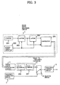
- a phase error detecting block in such a delay detector is illustrated in FIG. 3.
- the phase error measuring circuit 1 comprises a counter 201, a symbol timing detector 202, a pair of latches 203 and 204, and a subtractor 205.
- the symbol timing detector 202 detects and outputs a synchronizing symbol timing clock signal contained in a signal transmitted from a base.
- phase data are transmitted after delaying the phase of the data by one symbol period "T" after the phase at a time t0, and phase changes ⁇ /4, 3 ⁇ /4, - ⁇ /4, and -3 ⁇ /4 are assigned the 2-bit code data 00, 01, 10, and 11, respectively.
- Phase data are generated by the counter 201, which rotates one cycle per period of input signal applied thereto.
- the counter 201 applies an output signal to the latch 203, which latches the applied signal as n-bit parallel data in a timed relationship to one period of the synchronizing symbol clock signal from the symbol timing detector 202.
- the latch 204 latches the data which have been latched by the latch 203 in a previous period of the synchronizing symbol clock signal.
- the latches 203 and 204 apply their output signals to the subtractor 205, which produces phase difference information representing the phase difference between the output signals from the latches 203 and 204.
- the two highest-order bits correspond to phase information such as ⁇ /4, 3 ⁇ /4,... , described above, and the two lowest-order (n, n-1) bits correspond to a phase error.
- Phase error integrating circuit 2 Phase error integrating circuit 2:
- phase errors 1 Under white noise, the integrated value ideally becomes 0 as the phase errors 1 are integrated and canceled out in positive and negative directions. If phase errors have a frequency offset, they will be integrated in either a positive direction or a negative direction.
- An integrator used integrates the two lowest-order (n, n-1) inputted bits represented by two's complements, and, as a result, outputs a carry/borrow.
- the phase-to-frequency converter 3 converts the output signal from the phase error integrating circuit 2 to a frequency control signal, and outputs control data based on the frequency control signal to the frequency controller 9.
- the phase-to-frequency converter 3 comprises an U/D counter 206 for converting the output signal from the phase error integrating circuit 2 to a frequency control signal and a D/A converter 207 for outputting control data to the frequency controller 9.
- the frequency correcting circuit 7 detects a corrective change for a frequency error during reception slots and outputs frequency correcting pulses depending on the detected corrective change.
- the frequency correcting circuit 7 also determines the sign and magnitude of a change per unit time of integrated frequency errors, changes either one of positive and negative corrective outputs to correct the sign and magnitude, and changes a correcting interval.
- the frequency correcting circuit 7 is followed by a PLL circuit or a narrow bandpass filter for synchronizing a reference carrier with a carrier component.
- the output signals and interval of the frequency correcting circuit 7 may be multiplied by a certain coefficient depending on the characteristics of the PLL circuit or the narrow bandpass filter following the frequency correcting circuit 7.
- the frequency controller 9 is an oscillator whose frequency is variable according to a controlling quantity. Since the frequency controller 9 is usually equipped with a PLL, the controlling quantity is applied to the reference oscillator of the PLL.
- a signal received in the period of a reception slot is applied to the phase error measuring circuit 1 and converted thereby to phase error information from a symbol point.
- the phase error information is then outputted to the phase error integrating circuit 2.
- the integrated phase error value produced by the phase error integrating circuit 2 changes in either a positive direction or a negative direction.
- the output signal from the phase error integrating circuit 2 is converted to a frequency error by the phase-to-frequency converter 3.
- the output signal from the phase error integrating circuit 2 is also latched by the latches 4 and 5 in response to a change-detected signal Sck which rises two times between reception slots.
- the change-detected signal Sck is used for each of the latches 4 and 5 to detect a phase change at a desired time in the period of the reception slot to determine a phase change per set time.
- phase error integrated information outputted without pulse delay from latch 4 and the phase error integrated information outputted from latch 5 are applied to the subtractor 6.
- the subtractor 6 detects the difference between the applied phase error integrated information, i.e., the output signals from the latches 4 and 5 and outputs the detected difference to the frequency correcting circuit 7.
- a reception slot-detected signal Ssc will next be described.
- a known particular data pattern is inserted in a predetermined position in a transmitted slot.
- the receiver detects an assigned time slot from the particular data pattern and generates a signal as a reception slot-detected signal Ssc which remains high only during the detected time slot.
- the frequency correcting circuit 7 determines and outputs a frequency correcting value between reception slots based on the information representing the difference between the phase errors.
- the output signals from the phase-to-frequency converter 3 and the frequency correcting circuit 7 are supplied to the selector switch 8.
- the selector switch 8 is also supplied with the reception slot-detected signal Ssc, which is a signal for detecting a change in frequency converting operation between reception slots. Based on the reception slot-detected signal Ssc, the selector switch 8 confirms whether the present time is within the period of the reception slot or between reception slots.
- the selector switch 8 selects the output signal from the phase-to-frequency converter 3 and applies it to its output terminal. If the present time is between reception slots, the selector switch 8 selects the output signal from the frequency correcting circuit 7 and applies it to its output terminal. The selector switch 8 also outputs to the power supply circuit 12 a power supply control signal Spw indicative of which signal it is selecting.
- the power supply circuit 12 supplies electrical energy over the power line PL to the receiving circuit composed of the phase error measuring circuit 1, the phase error integrating circuit 2, and the phase-to-frequency converter 3 only during the time the power supply control signal Spw indicating that the selector switch 8 is selecting the output signal from the frequency correcting circuit 7.
- the frequency controller 9 is supplied with the output signal from the selector switch 8 and effects frequency control depending on the supplied output signal.
- the receiving circuit composed of the phase error measuring circuit 1, the phase error integrating circuit 2, and the phase-to-frequency converter 3 is supplied with electrical energy from the power supply circuit 12 in order to stabilize the frequency with the output signal from the receiving circuit.
- the frequency is stabilized by the output signal from the change detecting circuit 10. At this time, no electrical energy is supplied to the receiving circuit, and hence the consumption of electrical energy is reduced.
- the selector switch 8 which is supplied with the reception slot-detected signal Ssc, outputs the power supply control signal Spw indicative of the present selection based on the reception slot-detected signal Ssc, and the power supply circuit 12 determines whether it is to supply electrical energy or not depending on the power supply control signal Spw.
- the power supply circuit 12 may be supplied with the reception slot-detected signal Ssc and determine whether it is to supply electrical energy or not depending on the supplied reception slot-detected signal Ssc, whereas the selector switch 8 may only select one of the input signals without outputting the power supply signal Spw.
- the receiving circuit has a correcting circuit similar to the frequency correcting circuit 7.
- a common correcting circuit may be connected between the selector switch 8 and the frequency controller 9. Therefore, the present invention is not limited to the illustrated embodiment.
- the present invention offers the following advantages:
- the receiving circuit composed of a phase error measuring circuit, a phase error integrating circuit, and a phase-to-frequency converter is energized to control the frequency of the receiver with the integrated value of phase errors from the receiving circuit only in the period of a reception slot. Between reception slots, the frequency of the receiver is controlled according to changes in the phase error in the reception slot. Therefore, even when the frequency stabilizer is in continuous operation, the receiving circuit operates only in the period of the reception slot. As a result, the electrical energy consumed by the receiving circuit is reduced.
Landscapes
- Digital Transmission Methods That Use Modulated Carrier Waves (AREA)
- Mobile Radio Communication Systems (AREA)
- Transceivers (AREA)
- Superheterodyne Receivers (AREA)
- Synchronisation In Digital Transmission Systems (AREA)
Claims (5)
- Frequenzstabilisierer in einem Funkkommunikationssystem zum Übertragen eines durch Phasenumtasten bei einem Zeitmultiplexprozeß modulierten Signals, enthaltend:eine Phasenfehler-Meßschaltung (1) zum Messen eines Phasenfehlers zwischen einem von einem Empfänger während des Zeitraums eines Empfangsschlitzes empfangenen Signal und einem Symbolpunkt;eine Phasenfehler-Integrationsschaltung (2) zum Integrieren eines Ausgangssignals von der Phasenfehler-Meßschaltung (1);einen Phase-Frequenz-Wandler (3) zum Umwandeln eines Ausgangssignals von der Phasenfehler-Integrationsschaltung (2) in einen Frequenzfehler;eine Leistungsversorgungsschaltung (12) zum Zuführen elektrischer Energie zu der Phasenfehler-Meßschaltung (1), der Phasenfehler-Integrationsschaltung (2) und dem Phase-Frequenz-Wandler (3);eine Änderungserkennungsschaltung (10) zum Erkennen einer Änderung des Ausgangssignals von der Phasenfehler-Integrationsschaltung (2);eine Frequenzkorrekturschaltung (7) zum Vorhersagen einer Frequenzkorrekturgröße zwischen Empfangsschlitzen unter Verwendung eines Ausgangssignals von der Änderungserkennungsschaltung (10);einen Wählschalter (8) zum Empfangen der Ausgangssignale vom Phase-Frequenz-Wandler (3) und der Frequenzkorrekturschaltung (7), zum Auswählen des Ausgangssignals vom Phase-Frequenz-Wandler (3) und zum Ausgeben des ausgewählten Ausgangssignals an einen Ausgangsanschluß hiervon während des Zeitraums des Empfangsschlitzes sowie zum Auswählen des Ausgangssignals von der Frequenzkorrekturschaltung (7) und zum Ausgeben des ausgewählten Ausgangssignals an den Ausgangsanschluß zwischen den Empfangsschlitzen undeine Frequenzsteuereinrichtung (9) zum Steuern der Frequenz des Empfängers abhängig von einem Ausgangssignal vom Wählschalter (8);wobei die Leistungsversorgungsschaltung (12) eine Einrichtung zum Verhindern des Zuführens von elektrischer Energie zu der Phasenfehler-Meßschaltung, der Phasenfehler-Integrationsschaltung und dem Phase-Frequenz-Wandler zwischen den Empfangsschlitzen aufweist.
- Frequenzstabilisierer nach Anspruch 1, wobei der Wählschalter (8) weiter vorgesehen ist, um ein das aktuell ausgewählte Ausgangssignal angebendes Leistungsversorgungs-Steuersignal an die Leistungsversorgungsschaltung (12) auszugeben, und wobei die in der Leistungsversorgungsschaltung (12) enthaltene Verhinderungseinrichtung das Zuführen von elektrischer Energie zur Phasenfehler-Meßschaltung (1), zur Phasenfehler-Integrationsschaltung (2) und zum Phase-Frequenz-Wandler (3) verhindert, wenn der Leistungsversorgungsschaltung (12) vom Wählschalter (8) ein Leistungsversorgungs-Steuersignal zugeführt wird, das angibt, daß der Wählschalter (8) das Ausgangssignal von der Frequenzkorrekturschaltung (7) auswählt.
- Frequenzstabilisierer in einem Funkkommunikationssystem zum Übertragen eines durch Phasenumtasten bei einem Zeitmultiplexprozeß modulierten Signals, enthaltend:eine Phasenfehler-Meßschaltung (1) zum Messen eines Phasenfehlers zwischen einem von einem Empfänger während des Zeitraums eines Empfangsschlitzes empfangenen Signal und einem Symbolpunkt;eine Phasenfehler-Integrationsschaltung (2) zum Integrieren eines Ausgangssignals von der Phasenfehler-Meßschaltung (1);einen Phase-Frequenz-Wandler (3) zum Umwandeln eines Ausgangssignals von der Phasenfehler-Integrationsschaltung (2) in einen Frequenzfehler;eine Leistungsversorgungsschaltung (12) zum Zuführen elektrischer Energie zu der Phasenfehler-Meßschaltung (1), der Phasenfehler-Integrationsschaltung (2) und dem Phase-Frequenz-Wandler (3);eine Änderungserkennungsschaltung (10) zum Erkennen einer Änderung des Ausgangssignals von der Phasenfehler-Integrationsschaltung (2);einen Wählschalter (8) zum Empfangen der Ausgangssignale vom Phase-Frequenz-Wandler (3) und der Änderungserkennungsschaltung (10), zum Auswählen des Ausgangssignals vom Phase-Frequenz-Wandler (3) und zum Ausgeben des ausgewählten Ausgangssignals an einem Ausgangsanschluß hiervon während des Zeitraums des Empfangsschlitzes sowie zum Auswählen des Ausgangssignals von der Änderungserkennungsschaltung (10) und zum Ausgeben des ausgewählten Ausgangssignals an den Ausgangsanschluß zwischen den Empfangsschlitzen;eine gemeinsame Frequenzkorrekturschaltung zum Vorhersagen einer Frequenzkorrekturgröße unter Verwendung eines Ausgangssignals vom Wählschalter (8) undeine Frequenzsteuereinrichtung (9) zum Steuern der Frequenz des Empfängers abhängig von einem Ausgangssignal von der gemeinsamen Frequenzkorrekturschaltung;wobei die Leistungsversorgungsschaltung (12) eine Einrichtung zum Verhindern des Zuführens von elektrischer Energie zu der Phasenfehler-Meßschaltung (1), der Phasenfehler-Integrationsschaltung (2) und dem Phase-Frequenz-Wandler (3) zwischen den Empfangsschlitzen aufweist.
- Frequenzstabilisierer nach Anspruch 3, wobei der Wählschalter weiter vorgesehen ist, um ein das aktuell ausgewählwählte Ausgangssignal angebendes Leistungsversorgungs-Steuersignal an die Leistungsversorgungsschaltung auszugeben, und wobei die in der Leistungsversorgungsschaltung (12) enthaltene Verhinderungseinrichtung das Zuführen von elektrischer Energie zur Phasenfehler-Meßschaltung (1), zur Phasenfehler-Integrationsschaltung (2) und zum Phase-Frequenz-Wandler (3) verhindert, wenn der Leistungsversorgungsschaltung (12) vom Wählschalter (8) ein Leistungsversorgungs-Steuersignal zugeführt wird, das angibt, daß der Wählschalter (8) das Ausgangssignal von der Änderungserkennungsschaltung (10) auswählt.
- Frequenzstabilisierer nach einem der Ansprüche 1 bis 4, bei welchem die Änderungserkennungsschaltung (10) einen Subtrahierer (6) zum Erkennen der Differenz zwischen Phasenfehlern aufweist, die von der Phasenfehler-Integrationsschaltung (2) in der ersten und der zweiten Hälfte des Zeitraums des Empfangsschlitzes ausgegeben werden.
Applications Claiming Priority (3)
| Application Number | Priority Date | Filing Date | Title |
|---|---|---|---|
| JP273953/92 | 1992-10-13 | ||
| JP27395392 | 1992-10-13 | ||
| JP27395392 | 1992-10-13 |
Publications (3)
| Publication Number | Publication Date |
|---|---|
| EP0592978A2 EP0592978A2 (de) | 1994-04-20 |
| EP0592978A3 EP0592978A3 (de) | 1995-03-29 |
| EP0592978B1 true EP0592978B1 (de) | 1999-06-16 |
Family
ID=17534875
Family Applications (1)
| Application Number | Title | Priority Date | Filing Date |
|---|---|---|---|
| EP93116408A Expired - Lifetime EP0592978B1 (de) | 1992-10-13 | 1993-10-11 | Frequenzstabilisierer in einem Funkkommunikationssystem mit phasenumgetasteten Signalen |
Country Status (5)
| Country | Link |
|---|---|
| US (1) | US5388103A (de) |
| EP (1) | EP0592978B1 (de) |
| AU (1) | AU667959B2 (de) |
| CA (1) | CA2108207C (de) |
| DE (1) | DE69325332T2 (de) |
Families Citing this family (1)
| Publication number | Priority date | Publication date | Assignee | Title |
|---|---|---|---|---|
| US7209178B1 (en) * | 1999-09-21 | 2007-04-24 | Samsung Electronics, Co., Ltd. | Optical transfer system having a transmitter and a receiver |
Family Cites Families (7)
| Publication number | Priority date | Publication date | Assignee | Title |
|---|---|---|---|---|
| FR2226778B1 (de) * | 1973-04-20 | 1976-05-28 | Lannionnais Electronique | |
| JPS6335045A (ja) * | 1986-07-30 | 1988-02-15 | Nec Corp | 位相ヒツト補償装置 |
| JPS6369354A (ja) * | 1986-09-10 | 1988-03-29 | Sumitomo Electric Ind Ltd | 復調装置 |
| EP0387245B1 (de) * | 1987-11-06 | 1991-09-25 | Deutsche ITT Industries GmbH | Digitale dqpsk-decoderteilschaltung |
| GB2236922B (en) * | 1989-08-31 | 1993-02-24 | Multitone Electronics Plc | Frequency synthesisers |
| US5077794A (en) * | 1989-11-16 | 1991-12-31 | Verilink Corporation | Dual framing bit sequence alignment apparatus and method |
| US5115452A (en) * | 1990-08-02 | 1992-05-19 | At&T Bell Laboratories | Phase jitter correction arrangement |
-
1993
- 1993-10-11 EP EP93116408A patent/EP0592978B1/de not_active Expired - Lifetime
- 1993-10-11 AU AU48931/93A patent/AU667959B2/en not_active Ceased
- 1993-10-11 DE DE69325332T patent/DE69325332T2/de not_active Expired - Fee Related
- 1993-10-12 CA CA002108207A patent/CA2108207C/en not_active Expired - Fee Related
- 1993-10-13 US US08/135,408 patent/US5388103A/en not_active Expired - Fee Related
Also Published As
| Publication number | Publication date |
|---|---|
| US5388103A (en) | 1995-02-07 |
| EP0592978A3 (de) | 1995-03-29 |
| CA2108207C (en) | 1998-08-11 |
| CA2108207A1 (en) | 1994-04-14 |
| DE69325332D1 (de) | 1999-07-22 |
| DE69325332T2 (de) | 1999-11-04 |
| AU4893193A (en) | 1994-04-28 |
| AU667959B2 (en) | 1996-04-18 |
| EP0592978A2 (de) | 1994-04-20 |
Similar Documents
| Publication | Publication Date | Title |
|---|---|---|
| EP0451289B1 (de) | Referenzsignalgenerator und diesen enthaltenden digitaler Demodulator | |
| EP0969636B1 (de) | Trägerfolgesystem unter Anwendung eines Fehleroffsetfrequenzsignals | |
| AU677909B2 (en) | Apparatus and method for maximizing frequency offset tracking performance in a digital receiver | |
| US4301537A (en) | Means and method for maintaining synchronization of a spread spectrum or other receiver clock | |
| US5539355A (en) | Frequency-shift-keying detector using digital circuits | |
| US5612972A (en) | Spectrum spread signal reception with differential demodulation of spectrum spread demodulated components at each synchronous point and at a point always one symbol period later | |
| JPS62163441A (ja) | 復調器 | |
| JPH0748710B2 (ja) | 直接シーケンス拡散スペクトラム通信システム用の受信機 | |
| RU2216113C2 (ru) | Приемник сигнала для цифрового звукового вещания | |
| US5812614A (en) | Apparatus and method for maximizing frequency offset tracking performance in a digital receiver | |
| EP0558034B1 (de) | Digitaler Demodulator für TT/4-QPSK-Signale | |
| EP0738053B1 (de) | Automatische Frequenzkontrollschaltung zur Verwendung in einem mobilen Kommunikationssystem | |
| US5341402A (en) | Automatic frequency control method and device for use in receiver | |
| EP0551106B1 (de) | Frequenzwobbelsteuerungsvorrichtung | |
| US4575684A (en) | Differential phase shift keying receiver | |
| US6693956B1 (en) | Power amplifier having negative feedback circuit for transmitter | |
| US6259997B1 (en) | Signal power detection apparatus | |
| US5793250A (en) | Phase demodulator selectively using a first or a second detector | |
| US5612977A (en) | Automatic frequency control circuit for a receiver of phase shift keying modulated signals | |
| EP0259867B1 (de) | Demodulator für PSK-modulierte Signale | |
| EP1006660B1 (de) | Vorrichtung zur Wiedergewinnung und Identifizierung eines Taktsignals | |
| US5388103A (en) | Frequency stabilizer for use in phase-shift keying radio communications system | |
| EP0993160B1 (de) | Schaltung zur Trägerwiederherstellung | |
| US6618459B1 (en) | Radio communication device and method of bit synchronization pull-in in the same | |
| US5608762A (en) | Apparatus and method for automatic discriminator compensation in a FSK receiver |
Legal Events
| Date | Code | Title | Description |
|---|---|---|---|
| PUAI | Public reference made under article 153(3) epc to a published international application that has entered the european phase |
Free format text: ORIGINAL CODE: 0009012 |
|
| AK | Designated contracting states |
Kind code of ref document: A2 Designated state(s): DE FR GB IT NL SE |
|
| PUAL | Search report despatched |
Free format text: ORIGINAL CODE: 0009013 |
|
| AK | Designated contracting states |
Kind code of ref document: A3 Designated state(s): DE FR GB IT NL SE |
|
| 17P | Request for examination filed |
Effective date: 19950217 |
|
| 17Q | First examination report despatched |
Effective date: 19970408 |
|
| GRAG | Despatch of communication of intention to grant |
Free format text: ORIGINAL CODE: EPIDOS AGRA |
|
| GRAG | Despatch of communication of intention to grant |
Free format text: ORIGINAL CODE: EPIDOS AGRA |
|
| GRAG | Despatch of communication of intention to grant |
Free format text: ORIGINAL CODE: EPIDOS AGRA |
|
| GRAH | Despatch of communication of intention to grant a patent |
Free format text: ORIGINAL CODE: EPIDOS IGRA |
|
| GRAH | Despatch of communication of intention to grant a patent |
Free format text: ORIGINAL CODE: EPIDOS IGRA |
|
| GRAA | (expected) grant |
Free format text: ORIGINAL CODE: 0009210 |
|
| AK | Designated contracting states |
Kind code of ref document: B1 Designated state(s): DE FR GB IT NL SE |
|
| REF | Corresponds to: |
Ref document number: 69325332 Country of ref document: DE Date of ref document: 19990722 |
|
| ITF | It: translation for a ep patent filed | ||
| ET | Fr: translation filed | ||
| PLBE | No opposition filed within time limit |
Free format text: ORIGINAL CODE: 0009261 |
|
| STAA | Information on the status of an ep patent application or granted ep patent |
Free format text: STATUS: NO OPPOSITION FILED WITHIN TIME LIMIT |
|
| 26N | No opposition filed | ||
| PGFP | Annual fee paid to national office [announced via postgrant information from national office to epo] |
Ref country code: NL Payment date: 20001026 Year of fee payment: 8 |
|
| REG | Reference to a national code |
Ref country code: GB Ref legal event code: IF02 |
|
| PG25 | Lapsed in a contracting state [announced via postgrant information from national office to epo] |
Ref country code: NL Free format text: LAPSE BECAUSE OF NON-PAYMENT OF DUE FEES Effective date: 20020501 |
|
| NLV4 | Nl: lapsed or anulled due to non-payment of the annual fee |
Effective date: 20020501 |
|
| PGFP | Annual fee paid to national office [announced via postgrant information from national office to epo] |
Ref country code: SE Payment date: 20051005 Year of fee payment: 13 Ref country code: GB Payment date: 20051005 Year of fee payment: 13 |
|
| PGFP | Annual fee paid to national office [announced via postgrant information from national office to epo] |
Ref country code: DE Payment date: 20051006 Year of fee payment: 13 |
|
| PGFP | Annual fee paid to national office [announced via postgrant information from national office to epo] |
Ref country code: FR Payment date: 20051010 Year of fee payment: 13 |
|
| PG25 | Lapsed in a contracting state [announced via postgrant information from national office to epo] |
Ref country code: SE Free format text: LAPSE BECAUSE OF NON-PAYMENT OF DUE FEES Effective date: 20061012 |
|
| PGFP | Annual fee paid to national office [announced via postgrant information from national office to epo] |
Ref country code: IT Payment date: 20061031 Year of fee payment: 14 |
|
| PG25 | Lapsed in a contracting state [announced via postgrant information from national office to epo] |
Ref country code: DE Free format text: LAPSE BECAUSE OF NON-PAYMENT OF DUE FEES Effective date: 20070501 |
|
| EUG | Se: european patent has lapsed | ||
| GBPC | Gb: european patent ceased through non-payment of renewal fee |
Effective date: 20061011 |
|
| REG | Reference to a national code |
Ref country code: FR Ref legal event code: ST Effective date: 20070629 |
|
| PG25 | Lapsed in a contracting state [announced via postgrant information from national office to epo] |
Ref country code: GB Free format text: LAPSE BECAUSE OF NON-PAYMENT OF DUE FEES Effective date: 20061011 |
|
| PG25 | Lapsed in a contracting state [announced via postgrant information from national office to epo] |
Ref country code: FR Free format text: LAPSE BECAUSE OF NON-PAYMENT OF DUE FEES Effective date: 20061031 |
|
| PG25 | Lapsed in a contracting state [announced via postgrant information from national office to epo] |
Ref country code: IT Free format text: LAPSE BECAUSE OF NON-PAYMENT OF DUE FEES Effective date: 20071011 |