EP0593329A1 - Verfahren zum Verbesseren der Remanenzpolarisation einer Polymer Schicht und Anwendung in pyroelektrischer oder piezoelektrischer Wandler - Google Patents
Verfahren zum Verbesseren der Remanenzpolarisation einer Polymer Schicht und Anwendung in pyroelektrischer oder piezoelektrischer Wandler Download PDFInfo
- Publication number
- EP0593329A1 EP0593329A1 EP93402404A EP93402404A EP0593329A1 EP 0593329 A1 EP0593329 A1 EP 0593329A1 EP 93402404 A EP93402404 A EP 93402404A EP 93402404 A EP93402404 A EP 93402404A EP 0593329 A1 EP0593329 A1 EP 0593329A1
- Authority
- EP
- European Patent Office
- Prior art keywords
- layer
- temperature
- network
- annealing
- quenching
- Prior art date
- Legal status (The legal status is an assumption and is not a legal conclusion. Google has not performed a legal analysis and makes no representation as to the accuracy of the status listed.)
- Ceased
Links
- 238000000034 method Methods 0.000 title claims abstract description 30
- 229920000642 polymer Polymers 0.000 title claims abstract description 29
- 230000010287 polarization Effects 0.000 title claims description 19
- 238000000137 annealing Methods 0.000 claims abstract description 21
- 238000010791 quenching Methods 0.000 claims abstract description 16
- 230000000171 quenching effect Effects 0.000 claims abstract description 16
- 230000008018 melting Effects 0.000 claims abstract description 13
- 238000002844 melting Methods 0.000 claims abstract description 13
- 239000000758 substrate Substances 0.000 claims abstract description 12
- 238000004519 manufacturing process Methods 0.000 claims abstract description 7
- 230000005684 electric field Effects 0.000 claims abstract description 5
- 238000000151 deposition Methods 0.000 claims abstract description 3
- 230000008021 deposition Effects 0.000 claims abstract description 3
- 229920001343 polytetrafluoroethylene Polymers 0.000 claims description 15
- 239000004810 polytetrafluoroethylene Substances 0.000 claims description 15
- 239000000463 material Substances 0.000 claims description 13
- 238000002425 crystallisation Methods 0.000 claims description 11
- 230000008025 crystallization Effects 0.000 claims description 11
- 239000002861 polymer material Substances 0.000 claims description 8
- 229920001577 copolymer Polymers 0.000 claims description 7
- -1 Polytetrafluoroethylene Polymers 0.000 claims description 5
- MIZLGWKEZAPEFJ-UHFFFAOYSA-N 1,1,2-trifluoroethene Chemical group FC=C(F)F MIZLGWKEZAPEFJ-UHFFFAOYSA-N 0.000 claims description 4
- BQCIDUSAKPWEOX-UHFFFAOYSA-N 1,1-Difluoroethene Chemical compound FC(F)=C BQCIDUSAKPWEOX-UHFFFAOYSA-N 0.000 claims description 4
- 239000004065 semiconductor Substances 0.000 claims description 3
- 229920006126 semicrystalline polymer Polymers 0.000 claims description 3
- 238000001816 cooling Methods 0.000 claims description 2
- 238000001953 recrystallisation Methods 0.000 abstract 2
- 230000000694 effects Effects 0.000 description 8
- 239000013078 crystal Substances 0.000 description 5
- 238000001514 detection method Methods 0.000 description 4
- 230000005855 radiation Effects 0.000 description 4
- 239000004642 Polyimide Substances 0.000 description 3
- 230000004927 fusion Effects 0.000 description 3
- 230000008520 organization Effects 0.000 description 3
- 229920001721 polyimide Polymers 0.000 description 3
- 239000002904 solvent Substances 0.000 description 3
- 230000008020 evaporation Effects 0.000 description 2
- 238000001704 evaporation Methods 0.000 description 2
- 238000009987 spinning Methods 0.000 description 2
- 239000002033 PVDF binder Substances 0.000 description 1
- 230000002745 absorbent Effects 0.000 description 1
- 239000002250 absorbent Substances 0.000 description 1
- 230000003321 amplification Effects 0.000 description 1
- 230000015572 biosynthetic process Effects 0.000 description 1
- 238000006073 displacement reaction Methods 0.000 description 1
- 238000000407 epitaxy Methods 0.000 description 1
- 238000005530 etching Methods 0.000 description 1
- 239000012212 insulator Substances 0.000 description 1
- 239000011159 matrix material Substances 0.000 description 1
- 239000002184 metal Substances 0.000 description 1
- 238000001465 metallisation Methods 0.000 description 1
- 238000003199 nucleic acid amplification method Methods 0.000 description 1
- 230000003287 optical effect Effects 0.000 description 1
- 229920002981 polyvinylidene fluoride Polymers 0.000 description 1
- 230000005616 pyroelectricity Effects 0.000 description 1
- 230000035945 sensitivity Effects 0.000 description 1
- 238000009736 wetting Methods 0.000 description 1
Images
Classifications
-
- H—ELECTRICITY
- H03—ELECTRONIC CIRCUITRY
- H03H—IMPEDANCE NETWORKS, e.g. RESONANT CIRCUITS; RESONATORS
- H03H3/00—Apparatus or processes specially adapted for the manufacture of impedance networks, resonating circuits, resonators
-
- H—ELECTRICITY
- H10—SEMICONDUCTOR DEVICES; ELECTRIC SOLID-STATE DEVICES NOT OTHERWISE PROVIDED FOR
- H10N—ELECTRIC SOLID-STATE DEVICES NOT OTHERWISE PROVIDED FOR
- H10N15/00—Thermoelectric devices without a junction of dissimilar materials; Thermomagnetic devices, e.g. using the Nernst-Ettingshausen effect
- H10N15/10—Thermoelectric devices using thermal change of the dielectric constant, e.g. working above and below the Curie point
-
- H—ELECTRICITY
- H10—SEMICONDUCTOR DEVICES; ELECTRIC SOLID-STATE DEVICES NOT OTHERWISE PROVIDED FOR
- H10N—ELECTRIC SOLID-STATE DEVICES NOT OTHERWISE PROVIDED FOR
- H10N30/00—Piezoelectric or electrostrictive devices
- H10N30/01—Manufacture or treatment
- H10N30/04—Treatments to modify a piezoelectric or electrostrictive property, e.g. polarisation characteristics, vibration characteristics or mode tuning
- H10N30/045—Treatments to modify a piezoelectric or electrostrictive property, e.g. polarisation characteristics, vibration characteristics or mode tuning by polarising
-
- H—ELECTRICITY
- H10—SEMICONDUCTOR DEVICES; ELECTRIC SOLID-STATE DEVICES NOT OTHERWISE PROVIDED FOR
- H10N—ELECTRIC SOLID-STATE DEVICES NOT OTHERWISE PROVIDED FOR
- H10N30/00—Piezoelectric or electrostrictive devices
- H10N30/01—Manufacture or treatment
- H10N30/09—Forming piezoelectric or electrostrictive materials
- H10N30/098—Forming organic materials
Definitions
- the invention relates to a method for improving the polarization of a layer of polymer material and applications to transducers and in particular to pyroelectric transducers and piezoelectric transducers.
- Certain polymers such as polyvinylidene fluoride, and copolymers derived therefrom have particular characteristics of piezoelectricity and pyroelectricity.
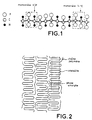
- the copolymer of vinylidene fluoride and of trifluoroethylene P has a molecular structure as shown in FIG. 1. It has a ferroelectric phase at room temperature and, at high temperature (higher than the Curie temperature), a paraelectric phase. It is therefore already apparent that the detection of the passage from the ferroelectric phase to the paraelectric phase makes it possible to produce a pyroelectric detector.
- linear polymers such as PVDF-TrFE
- PVDF-TrFE linear polymers
- the polarization is important.
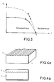
- FIG. 3 represents the variation of the remanent polarization Pr of a ferroelectric polymer material as a function of the temperature T. Inside the curve, the material is ferroelectric and outside the curve the material is paraelectric. To obtain good temperature detection, it is therefore necessary to be on a part of the curve having a significant slope at the point of detection. This means that for a determined material therefore having a determined Curie temperature Tc, it is advantageous to have a maximum remanent polarization (see dashed curve in FIG. 3). This is achieved by having a homogeneously polarized material. This polarization can result from a crystalline organization of the polymer.
- the invention provides a solution making it possible to impose a crystal orientation on a polymer layer in order to obtain maximum residual polarization of the material.
- the invention also makes it possible to increase the resistivity of the polymer layer.
- the annealing temperature linked to the duration of the annealing as well as the quenching temperature are of great importance so as to obtain a polymer layer having optimal polarization and resistivity.
- the network is produced by friction of the surface of the substrate using a polytetrafluoroethylene element.
- a network structure 2 of micron or submicron dimensions is produced on the surface of a substrate 1.
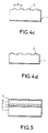
- This network can be a network of ridges as shown in FIG. 4a, or a continuous surface comprising a network of steps as shown in FIGS. 4c or 4d, or a combination of the two types of network.
- the space between two steps may be of the order of a few hundred nanometers (300 to 500 nm for example).
- a layer 3 of a polymer material is produced.
- the structure of FIG. 4b is obtained in which the network 2 has been shown to simplify in the form of a network of streaks. In this way, the molecular chains such as those of FIG. 1 tend to align in the streaks of the network 2. A crystal order is thus imposed.
- a fusion is first carried out, which will be called in the following an annealing of the polymer material. This annealing takes place at a temperature slightly above the melting temperature. Then a quenching operation is carried out at a temperature close to the crystallization temperature of the polymeric material. The orientation of the polymer molecules is thus imposed by the network 2.
- the network 2 is produced on a surface of a substrate (such as for example an amorphous semiconductor) which can be several square centimeters, by rubbing this surface with a PTFE (polytetrafluoroethylene) element so as to effect continuous deposits of PTFE and which thus form the network 2.
- a substrate such as for example an amorphous semiconductor
- PTFE polytetrafluoroethylene
- This operation is carried out at a temperature between 130 ° C and 300 ° C by exerting a pressure of approximately 1 Kg / cm2 and at a speed of friction displacement for example 1 mm / sec.
- the PTFE layer can be a few nanometers thick.
- the layer of polymeric material 3 is deposited according to a process such as that of the spinner with a thickness of a few micrometers for example (10 ⁇ m).
- the polymer contains a solvent.
- the solvent is therefore allowed to evaporate.
- an annealing is carried out by bringing the assembly to a temperature above the melting temperature of the polymer of at most 40 ° C. relative to the melting temperature.
- a quenching temperature will be chosen just below the rapid crystallization temperature, for example a few degrees (or even 1 or 2 degrees) below the crystallization temperature.
- a temperature of around 125 ° C. will be chosen. It is noted by this process that a regular crystalline organization of the polymer layer is obtained and the problem of wetting of PTFE is eliminated. In addition, a high resistivity is obtained.
- the annealing and quenching temperatures chosen in the temperature ranges indicated above are important in the context of the invention to obtain these results.
- This treatment therefore makes it possible to induce an oriented growth of the polymer by pseudo-epitaxy from the network 2 which makes the polymer fibrils grow from one step to another (or from one streak to another) with the axes.
- Layer 3 is then subjected to an electric field and is thus oriented electrically to give a residual polarization to the material and to obtain maximum pyroelectric and piezoelectric coefficients.
- the method described is applicable to the production of pyroelectric or piezoelectric transducers.
- one or more electrodes 4 are made on the surface of the substrate (FIG. 5).
- This electrode is preferably metallic, even transparent (ITO).
- an upper electrode 5 is produced which can also be transparent.
- this device can be used to detect radiation such as infrared radiation.
- the electrode 4 and the substrate 1, or the electrode 5 must then be transparent to the radiation to be detected.
- the invention therefore makes it possible to improve the performance of the pyroelectric imager in terms of sensitivity and thermal resolution.
- a 20% improvement in remanent polarization improves the thermal resolution of the imager by 20%.
- a CCD charge transfer read circuit is combined with a pyroelectric detector.
- the reading circuit was previously carried out according to the usual techniques known to those skilled in the art.
- On its upper part, it carries a set of electrodes which determines a network of detector points.
- a spinner a layer of polyimide 10 ⁇ m thick is deposited over it. This layer serves as a thermal insulator. Annealing at 300-400 ° C is then necessary to obtain a complete imidization of the polyimide.
- An etching step makes it possible to release holes plumb with the conductive studs. These holes are then metallized (evaporation of a metal under vacuum) in order to make them conductive.
- On the surface of the polyimide layer are made elementary electrodes each connected to a metallization. These electrodes correspond to the electrode 4 of FIG. 5 previously described.
- a layer of PTFE is now deposited by friction on the circuit previously heated to a temperature close to 300 ° C.
- the layer of pyroelectric polymer is then deposited by the spinning method.
- An annealing step can be carried out to evaporate the solvent under vacuum.
- the circuit is then heat treated as described above. That is to say, a circuit is then followed by quenching to recrystallize the layer with a high crystal orientation and high resistivity.
- a second electrode (corresponding to electrode 5 of FIG. 5) is then deposited on the polymer, by evaporation under vacuum to apply the electric field and induce the maximum remanent polarization.
- a layer of absorbent I.R. (intended to absorb the optical radiation to detect and to transmit the heat received to the polymer) is finally deposited on the electrode 5.
- the detector is then ready to function.
Landscapes
- Engineering & Computer Science (AREA)
- Manufacturing & Machinery (AREA)
- Treatments Of Macromolecular Shaped Articles (AREA)
- Photometry And Measurement Of Optical Pulse Characteristics (AREA)
Applications Claiming Priority (2)
| Application Number | Priority Date | Filing Date | Title |
|---|---|---|---|
| FR9212140 | 1992-10-12 | ||
| FR9212140A FR2696872B1 (fr) | 1992-10-12 | 1992-10-12 | Procédé d'amélioration de la polarisation rémanente d'une couche en matériau polymère et applications à des transducteurs pyroélectriques et piézoélectriques. |
Publications (1)
| Publication Number | Publication Date |
|---|---|
| EP0593329A1 true EP0593329A1 (de) | 1994-04-20 |
Family
ID=9434417
Family Applications (1)
| Application Number | Title | Priority Date | Filing Date |
|---|---|---|---|
| EP93402404A Ceased EP0593329A1 (de) | 1992-10-12 | 1993-10-01 | Verfahren zum Verbesseren der Remanenzpolarisation einer Polymer Schicht und Anwendung in pyroelektrischer oder piezoelektrischer Wandler |
Country Status (2)
| Country | Link |
|---|---|
| EP (1) | EP0593329A1 (de) |
| FR (1) | FR2696872B1 (de) |
Cited By (1)
| Publication number | Priority date | Publication date | Assignee | Title |
|---|---|---|---|---|
| FR2746416A1 (fr) * | 1996-03-22 | 1997-09-26 | Thomson Csf | Procede de realisation d'un film polymere cristallin oriente et appareil mettant en oeuvre ce procede |
Citations (2)
| Publication number | Priority date | Publication date | Assignee | Title |
|---|---|---|---|---|
| US4349502A (en) * | 1980-10-24 | 1982-09-14 | The United States Of America As Represented By The Secretary Of The Navy | Fabrication method for unoriented phase-I PVF2 |
| EP0087991A1 (de) * | 1982-02-22 | 1983-09-07 | Thomson-Csf | Verfahren zum Herstellen piezolektrischer polymerer Wandler durch Pressen |
-
1992
- 1992-10-12 FR FR9212140A patent/FR2696872B1/fr not_active Expired - Fee Related
-
1993
- 1993-10-01 EP EP93402404A patent/EP0593329A1/de not_active Ceased
Patent Citations (2)
| Publication number | Priority date | Publication date | Assignee | Title |
|---|---|---|---|---|
| US4349502A (en) * | 1980-10-24 | 1982-09-14 | The United States Of America As Represented By The Secretary Of The Navy | Fabrication method for unoriented phase-I PVF2 |
| EP0087991A1 (de) * | 1982-02-22 | 1983-09-07 | Thomson-Csf | Verfahren zum Herstellen piezolektrischer polymerer Wandler durch Pressen |
Cited By (1)
| Publication number | Priority date | Publication date | Assignee | Title |
|---|---|---|---|---|
| FR2746416A1 (fr) * | 1996-03-22 | 1997-09-26 | Thomson Csf | Procede de realisation d'un film polymere cristallin oriente et appareil mettant en oeuvre ce procede |
Also Published As
| Publication number | Publication date |
|---|---|
| FR2696872A1 (fr) | 1994-04-15 |
| FR2696872B1 (fr) | 1994-12-09 |
Similar Documents
| Publication | Publication Date | Title |
|---|---|---|
| US5372859A (en) | Enhanced fatigue and retention in ferroelectric thin film memory capacitors by post-top electrode anneal treatment | |
| EP1058837B1 (de) | Kapazitive sensoren zur messung der feuchtigkeit und deren verfahren zur herstellung | |
| EP3384257B1 (de) | Wärmemustersensor | |
| FR3044409A1 (fr) | Capteur de motif thermique comportant une portion pyroelectrique superieure a forte conductivite thermique | |
| EP0828145A1 (de) | Infrarot-Detektor und Verfahren zu dessen Herstellung | |
| EP0406053B1 (de) | Pyroelektrische Materialien enthaltende Infrarotfühler | |
| EP0371868B1 (de) | Monolithische Struktur für einen IR-Detektor oder IR-Bildsensor und Verfahren zu ihrer Herstellung | |
| FR2620531A1 (fr) | Detecteur thermique en reseau | |
| FR3044408A1 (fr) | Capteur de motif thermique a capacite pyroelectrique horizontale | |
| FR2759495A1 (fr) | Dispositif semiconducteur en polymere comportant au moins une fonction redresseuse et procede de fabrication d'un tel dispositif | |
| FR2989485A1 (fr) | Capteur tactile et procede de fabrication d'un tel capteur | |
| EP3492892A1 (de) | Thermischer mustersensor mit pyroelektrischer kapazität | |
| EP3483787A1 (de) | Verfahren zur durchführung einer stapelung von schichten für einen matrix-wärmesensor | |
| EP0593329A1 (de) | Verfahren zum Verbesseren der Remanenzpolarisation einer Polymer Schicht und Anwendung in pyroelektrischer oder piezoelektrischer Wandler | |
| FR3074575A1 (fr) | Capteur de motif thermique a capacite pyroelectrique | |
| EP3640615B1 (de) | Pyroelektrischer sensor mit verbesserter verkleidung des widerstands gegen abrieb | |
| EP3671871B1 (de) | Herstellungsverfahren einer vorrichtung, die ein material umfasst, das nach einer elektrischen polarisierung elektrische eigenschaften erwirbt | |
| EP3492891A1 (de) | Thermischer mustersensor mit pyroelektrischer kapazität, der eine sol-gel-matrix und metalloxidpartikel umfasst | |
| CH688596A5 (fr) | Procédé pour polariser au moins une zone d'une feuille de matériau ferroélectrique et application du procédé pour réaliser un élément polarisé pour capteur piézoélectrique ou pyroélectrique. | |
| FR3075953A1 (fr) | Capteur pyroelectrique avec blindage electro-magnetique ameliore. | |
| WO2018167394A1 (fr) | Detecteur pyroelectrique | |
| FR3107989A1 (fr) | Capteur de motif thermique dont la couche de protection surfacique presente une conduction thermique anisotrope | |
| JPS5932948B2 (ja) | 受光センサアレイ装置 | |
| FR3093658A1 (fr) | Procede pour deposer une couche en pvdf ou en un de ses copolymeres sur un substrat en verre ou en polymere | |
| FR3066017B1 (fr) | Dispositif pyroelectrique de detection infrarouge comportant un emetteur infrarouge de modulation |
Legal Events
| Date | Code | Title | Description |
|---|---|---|---|
| PUAI | Public reference made under article 153(3) epc to a published international application that has entered the european phase |
Free format text: ORIGINAL CODE: 0009012 |
|
| AK | Designated contracting states |
Kind code of ref document: A1 Designated state(s): BE CH DE FR GB IT LI NL |
|
| 17P | Request for examination filed |
Effective date: 19940801 |
|
| 17Q | First examination report despatched |
Effective date: 19960102 |
|
| GRAG | Despatch of communication of intention to grant |
Free format text: ORIGINAL CODE: EPIDOS AGRA |
|
| STAA | Information on the status of an ep patent application or granted ep patent |
Free format text: STATUS: THE APPLICATION HAS BEEN REFUSED |
|
| 18R | Application refused |
Effective date: 19980215 |