EP0593333B1 - Detektorzelle, Detektor, Sensor für Spektroskop - Google Patents
Detektorzelle, Detektor, Sensor für Spektroskop Download PDFInfo
- Publication number
- EP0593333B1 EP0593333B1 EP93402425A EP93402425A EP0593333B1 EP 0593333 B1 EP0593333 B1 EP 0593333B1 EP 93402425 A EP93402425 A EP 93402425A EP 93402425 A EP93402425 A EP 93402425A EP 0593333 B1 EP0593333 B1 EP 0593333B1
- Authority
- EP
- European Patent Office
- Prior art keywords
- quasi
- cell
- superconducting
- photon
- particles
- Prior art date
- Legal status (The legal status is an assumption and is not a legal conclusion. Google has not performed a legal analysis and makes no representation as to the accuracy of the status listed.)
- Expired - Lifetime
Links
- 239000002245 particle Substances 0.000 claims description 77
- 238000001514 detection method Methods 0.000 claims description 60
- 239000010955 niobium Substances 0.000 claims description 23
- 229910052758 niobium Inorganic materials 0.000 claims description 22
- GUCVJGMIXFAOAE-UHFFFAOYSA-N niobium atom Chemical compound [Nb] GUCVJGMIXFAOAE-UHFFFAOYSA-N 0.000 claims description 22
- 239000000463 material Substances 0.000 claims description 17
- 229910052782 aluminium Inorganic materials 0.000 claims description 16
- XAGFODPZIPBFFR-UHFFFAOYSA-N aluminium Chemical compound [Al] XAGFODPZIPBFFR-UHFFFAOYSA-N 0.000 claims description 16
- 238000012545 processing Methods 0.000 claims description 16
- 230000005855 radiation Effects 0.000 claims description 12
- 239000000758 substrate Substances 0.000 claims description 7
- 239000011159 matrix material Substances 0.000 claims description 6
- 230000002829 reductive effect Effects 0.000 claims description 5
- 238000001228 spectrum Methods 0.000 claims description 5
- 238000005070 sampling Methods 0.000 claims description 4
- 238000007493 shaping process Methods 0.000 claims description 3
- 230000005670 electromagnetic radiation Effects 0.000 claims description 2
- 230000000694 effects Effects 0.000 description 41
- 230000003993 interaction Effects 0.000 description 30
- 230000006870 function Effects 0.000 description 20
- 230000005641 tunneling Effects 0.000 description 19
- 239000002887 superconductor Substances 0.000 description 18
- 238000005286 illumination Methods 0.000 description 11
- 238000010521 absorption reaction Methods 0.000 description 10
- 230000003595 spectral effect Effects 0.000 description 10
- 238000010586 diagram Methods 0.000 description 9
- 230000002123 temporal effect Effects 0.000 description 8
- 230000004888 barrier function Effects 0.000 description 7
- 238000009792 diffusion process Methods 0.000 description 7
- 238000000695 excitation spectrum Methods 0.000 description 7
- 230000006798 recombination Effects 0.000 description 7
- 238000005215 recombination Methods 0.000 description 7
- 239000003990 capacitor Substances 0.000 description 6
- 230000007423 decrease Effects 0.000 description 6
- 230000001427 coherent effect Effects 0.000 description 5
- 230000002745 absorbent Effects 0.000 description 4
- 239000002250 absorbent Substances 0.000 description 4
- 238000000429 assembly Methods 0.000 description 4
- 239000010408 film Substances 0.000 description 4
- RYGMFSIKBFXOCR-UHFFFAOYSA-N Copper Chemical compound [Cu] RYGMFSIKBFXOCR-UHFFFAOYSA-N 0.000 description 3
- 230000003321 amplification Effects 0.000 description 3
- 238000004364 calculation method Methods 0.000 description 3
- 229910052802 copper Inorganic materials 0.000 description 3
- 239000010949 copper Substances 0.000 description 3
- 238000005259 measurement Methods 0.000 description 3
- 238000003199 nucleic acid amplification method Methods 0.000 description 3
- 238000006862 quantum yield reaction Methods 0.000 description 3
- 230000004044 response Effects 0.000 description 3
- 229910052594 sapphire Inorganic materials 0.000 description 3
- 239000010980 sapphire Substances 0.000 description 3
- 238000000926 separation method Methods 0.000 description 3
- 238000013019 agitation Methods 0.000 description 2
- 230000000903 blocking effect Effects 0.000 description 2
- 239000002800 charge carrier Substances 0.000 description 2
- 238000006243 chemical reaction Methods 0.000 description 2
- 230000008878 coupling Effects 0.000 description 2
- 238000010168 coupling process Methods 0.000 description 2
- 238000005859 coupling reaction Methods 0.000 description 2
- 230000005284 excitation Effects 0.000 description 2
- 230000000670 limiting effect Effects 0.000 description 2
- MYWUZJCMWCOHBA-VIFPVBQESA-N methamphetamine Chemical compound CN[C@@H](C)CC1=CC=CC=C1 MYWUZJCMWCOHBA-VIFPVBQESA-N 0.000 description 2
- 230000003287 optical effect Effects 0.000 description 2
- 230000009467 reduction Effects 0.000 description 2
- 239000004065 semiconductor Substances 0.000 description 2
- 230000003044 adaptive effect Effects 0.000 description 1
- 230000002238 attenuated effect Effects 0.000 description 1
- 230000005540 biological transmission Effects 0.000 description 1
- 230000008859 change Effects 0.000 description 1
- 230000005465 channeling Effects 0.000 description 1
- 238000004891 communication Methods 0.000 description 1
- 238000001816 cooling Methods 0.000 description 1
- 230000003247 decreasing effect Effects 0.000 description 1
- 230000001934 delay Effects 0.000 description 1
- 239000002270 dispersing agent Substances 0.000 description 1
- 230000008030 elimination Effects 0.000 description 1
- 238000003379 elimination reaction Methods 0.000 description 1
- 230000005281 excited state Effects 0.000 description 1
- 238000002474 experimental method Methods 0.000 description 1
- 230000005669 field effect Effects 0.000 description 1
- 239000003574 free electron Substances 0.000 description 1
- 230000005283 ground state Effects 0.000 description 1
- 238000009413 insulation Methods 0.000 description 1
- 238000004519 manufacturing process Methods 0.000 description 1
- 230000007246 mechanism Effects 0.000 description 1
- 229910052751 metal Inorganic materials 0.000 description 1
- 239000002184 metal Substances 0.000 description 1
- 230000005012 migration Effects 0.000 description 1
- 238000013508 migration Methods 0.000 description 1
- 230000004297 night vision Effects 0.000 description 1
- TWNQGVIAIRXVLR-UHFFFAOYSA-N oxo(oxoalumanyloxy)alumane Chemical compound O=[Al]O[Al]=O TWNQGVIAIRXVLR-UHFFFAOYSA-N 0.000 description 1
- 230000000704 physical effect Effects 0.000 description 1
- 238000007639 printing Methods 0.000 description 1
- 238000005295 random walk Methods 0.000 description 1
- 230000002441 reversible effect Effects 0.000 description 1
- 230000035945 sensitivity Effects 0.000 description 1
- 239000007787 solid Substances 0.000 description 1
- 239000010409 thin film Substances 0.000 description 1
- 238000003325 tomography Methods 0.000 description 1
- 238000012546 transfer Methods 0.000 description 1
- 229910052720 vanadium Inorganic materials 0.000 description 1
Images







Classifications
-
- H—ELECTRICITY
- H10—SEMICONDUCTOR DEVICES; ELECTRIC SOLID-STATE DEVICES NOT OTHERWISE PROVIDED FOR
- H10N—ELECTRIC SOLID-STATE DEVICES NOT OTHERWISE PROVIDED FOR
- H10N60/00—Superconducting devices
- H10N60/80—Constructional details
- H10N60/84—Switching means for devices switchable between superconducting and normal states
-
- H—ELECTRICITY
- H10—SEMICONDUCTOR DEVICES; ELECTRIC SOLID-STATE DEVICES NOT OTHERWISE PROVIDED FOR
- H10N—ELECTRIC SOLID-STATE DEVICES NOT OTHERWISE PROVIDED FOR
- H10N60/00—Superconducting devices
- H10N60/10—Junction-based devices
-
- Y—GENERAL TAGGING OF NEW TECHNOLOGICAL DEVELOPMENTS; GENERAL TAGGING OF CROSS-SECTIONAL TECHNOLOGIES SPANNING OVER SEVERAL SECTIONS OF THE IPC; TECHNICAL SUBJECTS COVERED BY FORMER USPC CROSS-REFERENCE ART COLLECTIONS [XRACs] AND DIGESTS
- Y10—TECHNICAL SUBJECTS COVERED BY FORMER USPC
- Y10S—TECHNICAL SUBJECTS COVERED BY FORMER USPC CROSS-REFERENCE ART COLLECTIONS [XRACs] AND DIGESTS
- Y10S505/00—Superconductor technology: apparatus, material, process
- Y10S505/825—Apparatus per se, device per se, or process of making or operating same
- Y10S505/848—Radiant energy application
Definitions
- the present invention relates mainly to a cell detection, to a matrix detector using such cells, to a sensor comprising such a detector and a spectroscope comprising such a sensor.
- Photon amplifier counting devices light have a low temporal resolution and show no spectral resolution.
- This type of detector can therefore have no resolution temporal as for the arrival of the various individual photons. Likewise, it is impossible to know the energy of each photon (no resolution spectral).
- a detection as defined in claim 1 comprising a superconductive element, in particular the element photosensitive in which the energy of each quasi particle coming from the broken Cooper pair decreases during interactions resulting in multiplication the number of quasi-particles, which increases extremely important the probability of detection of the interaction between a photon and the photosensitive element.
- one implements a detection cell comprising a superconductive sensitive element whose surface is large compared to the surface of one or, advantageously, tunnel effect detection junction (s).
- Superconductive channels having a forbidden band of 2 ⁇ , narrower than that of the sensitive element, channel quasi-particles to be detected towards the detection junctions.
- the main object of the invention is a photon detection cell comprising a niobium superconductive element sensitive to the photon of the radiation to be detected or to the phonons generated by such a photon, by separation of the Cooper pair into quasi-particles and a junction.
- superconducting tunnel effect comprising a superconductive electrode, the photosensitive superconductive element having characteristics at working temperature, of prohibited bandwidth of the excitation spectrum 2 ⁇ and of thickness allowing a reduction in the energy of each quasi particle from the broken Cooper pair with multiplication of the number of quasi-particles by a factor between 100 and 1000 in the spectrum from the near infrared to the ultraviolet and in that it is delimited by a plurality of superconductive effect junctions spaced tunnel, distributed at the periphery of the cell, characterized in that the cell comprises at the periphery, walls leading to the superconductive junctions with tunnel effect, made of a superconductive material, in particular of Al, the width of the forbidden band of the excitation spectrum 2 ⁇ 2 is less than the width 2 ⁇ 1 of the forbidden band of the excitation spectrum of the material of the sensitive element, so that said walls form channels to channel the quasi particles towards the superconductive junctions with tunnel effect and that the number of quasi particles increases after the passage of a quasi-particle of the sensitive element in a wall.
- the invention also relates to a cell, characterized in that the walls have discontinuities, preferably midway between two adjacent superconducting tunnel effect junctions.
- the invention also relates to a cell according to one any one of the preceding claims, characterized in that the element sensitive to a small thickness and is deposited on a substrate transparent to electromagnetic radiation to be captured.
- the invention also relates to a cell, characterized in that that it comprises a thin layer absorbing the radiation at capture, said layer being disposed between the support and the sensitive element.
- the invention also relates to a cell, characterized in that the superconductive tunnel junction is made of aluminum covered by a bonding layer of niobium electrode.
- the invention also relates to a detector, characterized in that that it comprises a plurality of cells, in particular a linear detector comprising cells aligned along an axis or a matrix detector with cells aligned in rows and columns.
- the invention also relates to a sensor comprising a cell or a detector, characterized in that it comprises an amplifier with low noise connected to each superconductive tunnel junction for amplify the current of quasi particles passing through tunnel effect through the junction.
- the invention also relates to a sensor, characterized in that that it includes analog digital converters ensuring the digitization of the signals delivered by the amplifiers and means of processing and / or storage of the digitized signal.
- the invention also relates to a sensor, characterized in what it includes coding means delivering for each value digital signal strength delivered by an amplifier, information concerning the position of the tunneling superconducting junction concerned, the reception time and the value of the current intensity amplified.
- the invention also relates to a sensor, characterized in that that it includes means for formatting the signal and means for calculation of determination according to the form of the signal transmitted by the means of shaping of the signal of the charge induced by the photon to be detected in the superconductive tunnel effect junction.
- the invention also relates to a sensor, characterized in what it means means of sampling the signal over intervals of time corresponding to the detection of successive photons and means to deduce the individual energy of each of the photons.
- the invention also relates to a sensor, characterized in that that it includes means for integrating the charge induced in a superconductive tunnel effect junction by a plurality of photons.
- the invention also relates to a spectroscope, characterized in that it comprises a sensor.
- a detector of known type comprising a first electrode 2 made of epitaxial niobium on a support 1 of sapphire forming an entrance window transparent to X-rays.
- a barrier 3 constituted by a layer of aluminum , a layer of aluminum oxide (Al O x ) and a layer of aluminum is interposed between the first electrode 2 and a second electrode 4 made of polycrystalline niobium.
- a first connection electrode 5 made of niobium is connected to the second electrode 4, while being isolated from the first electrode 2 by an insulating layer 6 made of Al O x .
- a second connection electrode 47, made of niobium, is connected to the first electrode 2.
- a superconducting tunnel effect junction (Superconducting Tunnel Junction or STJ in Anglo-Saxon terminology) is established through barrier 3 between the first electrode 2 and the second electrode 4 on the most of the surface of the detector.
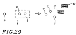
- FIGS. 2 to 6 and 29 we can see, diagrammatically, some interactions occurring in a detector according to the present invention. On the left side of Figures 2 to 6 and 29, the interacting elements and on the right side, we illustrated the result of interaction.
- the BCS quantum microscopic theory due to Bardeen, Cooper and Schrieffer, describes how the 7 electrons, which are Fermions (spin 1/2), minimize their energy by teaming up two by two to form pairs of Cooper 8 which are bosons (whole spin).
- This ordered state results of the existence, in a superconductor, of an attraction between electrons, by through the vibrations of the atomic network. This attraction is greater than the electrostatic repulsion forces between two electrons of same charge.
- FIG. 6 one can see the passage of a quasi particle 7 ′ between a first superconductor 12, for example niobium, having a first band gap 2 ⁇ 1 , towards a second superconductor material 13, for example aluminum having a second width 2 ⁇ 2 of the forbidden band of the excitation spectrum, less than 2 ⁇ 1 .
- the passage of the quasi-particle 7 'between the media 12 and the media 13 generates a phonon 10 which, by the mechanism illustrated in FIG. 3, will generate other quasi-particles 7' by breaking other pairs of Cooper 8.
- the passage of niobium, whose ⁇ is equal to 1.5 meV (1 eV is equal to 1.602 10 -19 J), towards aluminum, whose ⁇ is equal to 0.3 meV, corresponds to the multiplication of the number of quasi particles 7 'by a factor equal to 4.5.
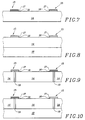
- a sensitive element superconductor 14 in which space cells have been defined by tunneling superconducting junctions 15 comprising an insulating barrier thin 16 and a superconductive electrode 17.
- the sensitive element 14 has a thickness and a rigidity sufficient to constitute the mechanical structure of cells and / or detector or rests on a substrate located on the rear face of the detector (not represented).
- the sensitive element can form a support either above or below the junctions.
- the element sensitive 14 was deposited on a rigid substrate 18 transparent to radiation of the frequency band in which we want to be able detect photons.
- the substrate 18 must be compatible with the materials of element 14 including at the very low temperatures necessary for the establishment of superconductivity.
- the niobium sensitive element it is possible, for example, to use sapphire for the detection of visible photons. It is possible to use a support 18 in sapphire while for a detection which has to extend into the ultraviolet, Mg F 2 is used .
- FIG. 9 which refers to a large spacing of the junctions
- a detector according to the present invention comprising walls 19 materializing the boundary between the detection cells and forming channels channeling the quasi particles 7 'to the junctions tunneling superconductors 15.
- the walls 19 are made of a material superconductor whose width of the forbidden band of the excitation spectrum is less than the width of the forbidden band of the element sensitive superconductor 14.
- the walls 19 are advantageously made of aluminum.
- the device of figure 11 presents a temporal resolution very high.
- the detection cell and the detector according to the present invention have a quantum efficiency close to 1 when a photon is absorbed by the sensitive element 14 or by the absorbent layer 20.
- the quantum efficiency is always close of 1, but we will have a higher quantity of quasi particles, and the answer is limited to a single junction.
- a detector according to the present invention comprising a matrix of square cells 21. It is understood that other forms of cells 21, such as triangular, hexagonal or circular, do not depart from the scope of the present invention. Similarly, without departing from the scope of the present invention, it is possible to produce a detector comprising only a single cell comprising one or more junction (s) tunneling superconductor (s).
- each cell 21 is delimited by four superconductive tunnel effect junctions 15 and by four walls 19 leading to the junctions 15 and arranged in a square.
- an interval 22 equidistant from two junctions 15 adjacent is formed in each wall 19.
- a quasi particle entering a wall 19 is channeled towards the superconductive junction at nearest tunnel effect.
- the presence of the aluminum walls 19 allows, on the other hand, to improve the time resolution by limiting the time included between the absorption of the photon and the detection of the signal by confining the quasi particles, and therefore a limitation of the propagation path of quasi particles.
- Superconductive tunnel junction 15 is shared between four cells 21, while a wall 19 is adjoining between two cells 21.
- Each tunnel effect superconductive junction 15 is connected to a low noise amplifier to amplify the current of quasi 7 'particles passing through tunnel effect.
- the amplifiers are directly broadcast in a semiconductor wafer with the same not only the tunneling superconducting junctions 15, the semiconductor wafer being brought into contact with the superconductive junctions at tunnel effect 15 of the structure of FIG. 12.
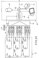
- FIG 13 we can see an example of an sensor according to the present invention comprising four detection cells 2111, 2112, 2121 and 2122.
- Cell 2111 is delimited by junctions 1511, 1512, 1521 and 1522 tunneling superconductors.
- detection 2112 is delimited by superconductive tunnel effect junctions 1512, 1513, 1522 and 1523.
- the detection cell 2121 is delimited by the 1521, 1522, 1531 and 1532 tunneling superconducting junctions.
- detection cell 2122 is delimited by the superconductive junctions at tunnel effect 1522, 1523, 1532 and 1533.
- each superconductive tunnel junction are connected, in series, a low noise amplifier 23, a converter analog digital 24 and means 25 for coding and / or processing information.
- a threshold comparator 26 is interposed between the output of analog digital converters 24 and the input of means 25 for coding and / or processing information.
- the means 25 advantageously comprise a coding device 27 ensuring the association, with each detection signal of a value i of the intensity or of the energy proportional to the number of quasi-particles detected, the time detection t and the junction number or coordinates superconducting tunnel effect concerned.
- the coded data are passed to an arithmetic and logic unit 28 for storage in a mass memory 29 and / or for online or offline processing, displaying the results on a display device 30, printing on a printer 31 or transmission over a communication line 32 to a device not shown.
- a coding device 27 is associated with each superconductive effect junction tunnel. In such a case, it is advantageous to connect all of the coding devices 27 to an arithmetic and logic unit 28 by through a multiplexer.
- the outputs of the threshold comparators 26 are connected by through a multiplexer 33 to a single coding device 27.
- a very precise clock 34 ensures the synchronization of sampling and conversion of multiplexing and coding.
- the quasi particles pass by tunnel effect through these junctions for provide a signal which is amplified by low noise amplifiers 23 correspondents.
- amplifiers 23 there is a signal from, on the one hand, quasi free particles present in the material, from very weak to very low temperatures, and on the other hand, constituting the electronic noise of the amplifier 23. In case the distance between the junctions is reduced, one could make the detection directly at these junctions.
- the signals delivered by the amplifiers 23 are sampled and digitized.
- the threshold comparators 26 eliminate the weak signals corresponding only to the electronic noise of the amplifiers 23 and to the detection of broken Cooper pairs, independently of the absorption of a photon.
- Only the signals corresponding to the superconductive tunnel effect junctions 1511, 1512, 1521 and 1522 are transmitted via the multiplexer 33 to the coding device 27.
- the coding device 27 generates four data, each comprising an identification of the superconductive junction, the detection time and the intensity of the detected current.
- the arithmetic and logic unit 28 determines, from the coordinates of the tunneling superconducting junctions having transmitted a signal, which is (are) the cell (s) of detection which has (have) interacted with a photon incident.
- the arithmetic and logical unit deduces the spatial coordinates of the interaction between the photons and the detector, the time of the interaction and the energy (and therefore the wavelength) of the incident photon. The results are transmitted, displayed and / or stored.
- the arithmetic and logic unit 28 performs statistical processing making it possible to present the data collected in a given time interval.
- the arithmetic and logical unit 28 takes into account the intensity of the current at each tunneling superconducting junction to determine by interpolation of the coordinates of the point of incidence inside the cell having detected the photon.
- niobium for sensitive elements 14 and aluminum for the walls 19.
- a junction superconducting tunnel effect 15 with the sensitive element 14 made of aluminum and an aluminum electrode 17 'between which a barrier is interposed insulating thin 16.
- the junctions 15 tunneling superconductors are closer together, allowing increase the temporal resolution by decreasing the maximum path of the quasi particles to the nearest junction.
- this provision may, without departing from the scope of the present invention, be taken up with the exemplary embodiments illustrated in FIGS. 7 to 12.
- the present invention is in no way limited to the implementation of aluminum and niobium, for example the use of the element sensitive in Sn makes it possible to obtain more than 3000 quasi particles for the absorption of a 3 eV photon with a substantially spectral resolution equal to 8 nm.
- the presence of Cooper 8 pairs represents the ground state, while the presence of quasi particles 7 'corresponds to the excited state.
- the number of quasi-particles 7 'at a temperature T (absolute temperature) expressed in K is proportional to exp (- ⁇ / KT), K being the Boltzmann constant.
- the number of quasi particles 7 ′ is extremely low compared to the number of quasi particles generated during the interaction of a cell with a photon.
- the population of quasi particles 7 ' dependss on the population and the energy of the phonons 10. Insofar as the band gap of the excitation spectrum 2 ⁇ is less than h ⁇ D , h ⁇ D being the energy of Debye.
- the phonons 10 can in a system in relaxation (and not in equilibrium) have enough energy to participate in the passage between a pair of Cooper 8 and two quasi particles 7 '.
- the population of phonons 10 whose energy h ⁇ is greater than the band gap is coupled to the population of quasi particles.
- the high energy phonons are produced during the absorption of a photon ( Figure 2) and during the relaxation of quasi particles 7 'of high energy. Phonons, whose energy is less than the forbidden band, are produced in particular during the recombination of two quasi particles 7 'in a pair of Cooper.
- ⁇ c be the confinement time of quasi particles in a superconductive film.
- R nn is proportional to exp (2b / A)
- b being the thickness of the insulating barrier
- A being the surface of the superconductive junction with tunnel effect
- ⁇ c depends mainly on the superconductor used, on its thickness and thickness of the insulation but is independent of the temperature T.
- the phonons are lost when leaving the superconducting cells. These losses depend on the geometry of the detection cell, thicknesses of the films involved, size of the connection electrodes and acoustic couplings between the various elements of the detection cell.
- Example of embodiment photosensitive niobium elements having a surface of between 150 and 400 ⁇ m 2 , a thickness of between 50 and 300 nm, ⁇ c between 60 and 5000 ns ( ⁇ c equal to 60 ns for the lowest value of the resistance R nn equal to 0.6 ⁇ ) and the volume being equal to 20 ⁇ m 3 . It is likely that ⁇ c can be reduced to 10 ns by reducing the size of the junction. ⁇ ç can be further reduced by a factor of 2.5 which corresponds to the value ratio of N Ef of Nb with respect to Al. In solid niobium at a temperature below 2 Kelvin, ⁇ can be estimated at 1.747 ⁇ and F at 0.22.
- the signal-to-noise ratio can be improved by eliminating signals whose time course does not correspond to a signal from of the absorption of a photon.
- the energy resolution can be estimated at 0.1 eV corresponding to a spectral resolution of 13 nm to 400 nm, in the case of niobium.
- the spatial resolution depends on the size of the detection cells in the case of the presence of the walls 19 and on the diffusion of the quasi particles during the time ⁇ in the absence of these walls.
- the diffusion of quasi particles at a time t is a function of the average free path ⁇ qp and the Fermi speed v F.
- ⁇ the average free path
- v F the Fermi speed
- the preferred embodiment of the device according to the invention uses three materials for, respectively, the sensitive element 14, the walls 19 and the superconductive tunnel effect junctions 15 having bandwidths 2 ⁇ prohibited increasingly reduced to favor the transfer of quasi particles 7 '.
- the device according to the present invention can advantageously be implemented in a spectroscope.
- a sensor of the type is used directly of that illustrated in FIG. 13 advantageously comprising an important number of cells 21.
- the spectral resolution of the device of figure 13 comes directly from the energy resolution of the detector according to this invention.
- a spectroscope comprising a detector 35, advantageously linear, placed behind a device dispersant, for example a diffraction grating 36.
- the output of the junctions 15 is connected analogously to that of the device in FIG. 13, to a information storage and / or processing unit 25.
- the spectrometer in Figure 14 has excellent resolution spectral coming on the one hand from the presence of the diffraction grating 36 and of the spatial resolution of the detector 35 and, on the other hand, of the resolution spectral of this detector.
- the performances of a detector according to the present invention mainly depending on the characteristics of the detection cell, but can also be degraded by the noise generated by the amplifier 23 especially if the electric charge (number of quasi particles 7 ') generated by photon 9 detected is weak.
- the superconductive tunnel junction 15 is connected to a generator current 40, at the input supply terminal 41, at a first armature of a capacitor 42 and, via a Zener diode 43 to ground 44.
- the second armature of the capacitor 42 is connected to the grid of a field effect transistor 45 at a first armature of a capacitor 46 and at the input of a resistor 48.
- the second armature of the capacitor 46 and the output of the resistor 48 are connected to the terminal 49 to which is available the amplified output signal.
- a first electrode of the effect transistor field 45 for example the drain, is connected to ground 44.
- the second electrode of transistor 45 for example the source, is connected, on the one hand, to the input of an amplifier 50 and, on the other hand, via a resistor 51 at terminal + 41.
- the power supply terminals of amplifier 50 are connected to earth 44 and to terminal + 41.
- the output of amplifier 50 is connected to the output terminal 49 of the amplifier 23.
- the resistor 48 had a value of 300 M ⁇ while the capacitor 46 had a capacity of one pF.
- the amplifier 23 of FIG. 18 can be optimized for the measurement of the energy of the captured photon 9 using a time constant longer of the amplifier. On the contrary, by adopting a constant of short time for the amplifier, we reduce the delays between two photons likely to be detected. In the first case, so that we can reliably measure the load of the corresponding detection cell biunivocally to the energy of the photon, two successive photons must be separated by at least one micro second. In the second case, a constant amplifier time may be in the order of the relaxation time of superconductive tunnel effect junction, which does not allow measurement specifies the total charge induced by the photon in the detection cell.
- FIG. 19 The behavior of the amplifier 23 of figure 18 capable of accurately measuring the charge induced in the detection cell is illustrated in FIG. 19.
- the current I has been illustrated as a function of the time t delivered by the junction connected to the amplifier 23.
- the current substantially forms a square signal between the time t 1 and t 2 .
- FIG. 19b one can see the charge C as a function of time t in the detection cell.
- the time t 1 corresponds to the capture of a photon 9.
- t 1 and t 2 there is relaxation of the superconductive junction with tunnel effect 15 with amplification of the number of quasi-particles 7 '.
- t 3 there is the discharge of the junction 15 in the amplifier 23 with exponential reduction of the charge according to the formula Ae - t / ⁇ c ,
- ⁇ c being typically between 10 and 300 ⁇ s.
- the signal I delivered by the amplifier 23 as a function of time t.
- the signal being zero up to t 1 , it includes a negative alternation 52 between t 1 and t 2 followed by a positive alternation 53.
- positive alternation 53 it is determined by processing the signal in an arithmetic unit and logic 28 the total charge delivered by the superconductive tunnel junction 15.
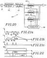
- the device of Figure 20 has a charge amplifier 54 connected to the output of the tunneling superconducting junction 15.
- the output of the amplifier 54 is connected to the input of a pole elimination device. Leaving the device 55 for eliminating poles is connected to the input of a device for control 56 and to the analog inputs of a series of samplers blockers 57, for example at the inputs of three blocker samplers 57.1, 57.2 and 57.3.
- the control device 56 is connected by lines of control to the various blocking samplers 57.
- the digital outputs blocking samplers 57 are connected, for example, by through the arithmetic and logic unit 28 to the storage unit 29.
- Figures 21a and 21b are similar to Figures 19a and 19b respectively, but illustrate the capture of three photons at times t 11 , t 21 and t 31 .
- the charge increases first of all between t 11 and t 12 following the relaxation of the junction 15 after the detection of the first photon and then decreases exponentially between t 12 and t 21 .
- the charge increases from the residual level of charges coming from the capture of the first photon, during the relaxation of the junction following the capture of the second photon.
- the total charge decreases exponentially.
- the residual charge increases during the relaxation of the junction 15 as a result of the capture of the third photon.
- the charge decreases exponentially until it reaches a zero value.
- FIG. 22c the corresponding poles have been represented detections of various photons.
- the functions 58.1 to 58.3 generated by the control device 56 and respectively controlling the samplers 57.1 to 57.3.
- the function 58.1 goes to the high level allowing the sampler 57.1 to ensure the sampling of the charge received, and this for example until time t 3 .
- the function 58.2 comprising a pulse when capturing the first photon goes to a low level and goes to a high level when the second photon is captured, for example up to t 3 .
- Function 58.3 comprises a pulse at the time of the capture of the second photon and a change to high level when the capture of the third photon.
- the arithmetic and logic unit 28 reconstructs the charges corresponding to the various photons by first calculating from the information available between t 12 and t 21 the charge generated by the interaction with the first photon. Then, by subtracting this charge from the charge measured at t 22 and t 31, the arithmetic and logic unit 28 determines the charge generated by the interaction with the second photon. Similarly by subtracting the charge from the second photon, the arithmetic and logic unit determines the charge generated during the interaction with the third photon.
- FIG. 23 An example of an amplifier 23 capable of delivering an analog signal indicating the intensity of the illumination of a detection cell is illustrated in FIG. 23 which is substantially identical to the amplifier 23 of FIG. 18 completed at its output 49 by an integrating circuit 59 comprising for example a resistor 60 placed in series with a capacitor 61 disposed between the output of the resistance 60 and ground 44.
- the amplifier 23 in FIG. 23 can be switched according to the instantaneous illumination levels, between the measurement of the individual energies of incident photons delivered to the terminal 49 and the value of a continuous illumination delivered at the output of the circuit integrator 59.
- a curve 64 representing a signal, for example a voltage V, as a function of time, the value of which indicates the illumination received by the detection cell according to the present invention.
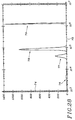
- Figures 25 to 28 show performances obtained with a prototype detection cell comprising a single superconducting junction with square tunnel effect of 12 ⁇ m side in niobium working at 0.3 K.
- the superconducting tunnel junction was connected to an amplifier 23 generating significant noise, which did not allow in this experiment to highlight photon counting individual.
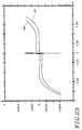
- Curve 65 corresponds to the intensity of the current in function of the bias voltage for a detection cell not illuminated.
- Curve 66 corresponds to the intensity of the current as a function of the voltage for a cell illuminated by radiation at 1,000 nm. Looking at curve 65, we can see that the current through the superconductive tunnel junction 15 is appreciably negligible for a bias voltage of less than 0.3 mv. This tension will therefore advantageously adopted as bias voltage of the junction superconducting tunnel effect. The difference in intensity I between the curves 66 and 65 is extremely important for detecting illumination of the cell.
- a division of the time scale t corresponds to 100 ⁇ s (divided into 10 subdivisions of 10 ⁇ s).
- the three curves 71, 72 and 73 are offset in the directions of voltages V relative to each other.
- a division of the scale of voltages V corresponds to 10 mV (divided into 10 subdivisions of 1 mV).
- the curve 71 corresponds to the noise in the absence of illumination.
- Curve 72 corresponds to a pulse of photons whose wavelength is substantially equal to 400 nm.
- the pulses have a duration of one ⁇ s and correspond to several hundred photons.
- the spread over time of the curves 72 and 73 is explained by the response time of the chain amplifier connected to the output of the superconductive effect junction tunnel, the physical effect at the level of the detection cell being of the order of the ⁇ s.
- Curves 72 and 73 prove the possibility of setting uses detection cells according to the present invention for detection short photon pulses for low levels of illumination with a broad spectrum.
- the device comprises two identical sub-assemblies 37 each comprising a small diameter telescope 38 at the outlet of which is placed a sensor according to the present invention, for example the sensor illustrated in FIG. 13.
- the clocks 34 of sub-assemblies 37 operate synchronously during data acquisition. This synchronism is obtained either by a synchronization of the clocks 34 with one another, or by a master clock, either by extreme precision of these clocks, for example using atomic clocks.
- the sub-assemblies 37 of an interferometer of FIG. 15 are placed at a distance which can vary between a hundred meters and a few hundred kilometers or more.
- the 38 telescopes of the sub-assemblies 37 are pointed with great precision in the same site and deposit management.
- a sensor according to the present invention can be put at the exit of a traditional telescope to allow the observation of a star low or very low magnitude.
- the implementation of the device according to the present invention collects additional information by compared to the known type device while reducing the exposure time, this which allows more observations to be made with the same telescope.
- the device according to the present invention applies to photon counting, and therefore mainly for acquisition and processing information from weak radiation sources.
- the invention mainly applies to astronomy, it can also be used for medical applications (attenuated light detection, tomography, etc.), image acquisitions in the atmosphere (coherent detection, photography, adaptive optics), night vision devices or the like.
Landscapes
- Measurement Of Radiation (AREA)
- Superconductor Devices And Manufacturing Methods Thereof (AREA)
- Medicines That Contain Protein Lipid Enzymes And Other Medicines (AREA)
- Medicines Containing Antibodies Or Antigens For Use As Internal Diagnostic Agents (AREA)
Claims (13)
- Photonendetektorzelle mit einem supraleitenden Element (14) aus Niob, das das Photon (9) der zu erfassenden Strahlung oder die Phonone (10) misst, die durch ein solches Photon (9) erzeugt werden, durch Aufteilung des Cooperpaars (8) in Quasiteilchen (7') und einen supraleitenden Übergang mit Tunneleffekt (15), der eine supraleitende Elektrode (17) umfasst, wobei das supraleitende photosensible Element, das Eigenschaften zur Betriebstemperatur, der unzulässigen Bandbreite des Anregungsspektrums (2Δ) und der Dicke hat, eine Energiesenkung jedes Quasiteilchens (7') zulässt, das aus dem Cooperpaar (8) hervorgegangen ist, das unter Multiplikation der Anzahl an Quasiteilchen mit einem zwischen 100 und 1000 im Spektrum vom nahen Infrarot bis Ultraviolett liegenden Faktor aufgebrochen wird, und wobei die Zelle durch mehrere beabstandete supraleitende Übergänge mit Tunneleffekt (15) begrenzt ist, die auf dem Zellenumfang (21) verteilt sind, dadurch gekennzeichnet, dass die Zelle am Umfang Wände (19) aufweist, die an die supraleitenden Übergänge mit Tunneleffekt (15) angrenzen, und ein supraleitendes Material, d. h. Al, dessen unzulässige Bandbreite des Anregungsspektrums 2Δ2 kleiner ist als die unzulässige Bandbreite des Anregungsspektrums 2Δ1 des Materials des sensiblen Elements (14), so dass die Wände (19) Kanäle bilden, um die Quasiteilchen (7') zu den supraleitenden Übergängen mit Tunneleffekt (15) zu leiten, und dass die Anzahl der Quasiteilchen (7') nach dem Durchgang eines Quasiteilchens (7') des sensiblen Elements (14) in einer Wand (19) ansteigt.
- Zelle nach Anspruch 1, dadurch gekennzeichnet, dass die Wände (19) Unterbrechungen (22) aufweisen, vorzugsweise auf halber Entfernung zwischen zwei benachbarten supraleitenden Übergängen mit Tunneleffekt (15).
- Zelle nach einem der vorhergehenden Ansprüche, dadurch gekennzeichnet, dass das sensible Element (14) eine geringe Dicke hat und auf einem Substrat (18) untergebracht ist, das für die zu erfassende elektromagnetische Strahlung durchlässig ist.
- Zelle nach Anspruch 3, dadurch gekennzeichnet, dass sie eine Schicht (20) geringer Dicke umfasst, die die zu erfassende Strahlung absorbiert, wobei die Schicht (20) zwischen dem Träger (18) und dem sensiblen Element (14) angeordnet ist.
- Zelle nach einem der vorhergehenden Ansprüche, dadurch gekennzeichnet, dass der supraleitende Übergang mit Tunneleffekt (15) aus Aluminium besteht, das mit einer Elektrodenbefestigungsschicht aus Niob (17, 14') beschichtet ist.
- Detektor, dadurch gekennzeichnet, dass er mehrere Zellen (21) nach einem der vorhergehenden Ansprüche umfasst, insbesondere linearer Detektor mit in einer Achse ausgerichteten Zellen (21) oder Matrixdetektor mit in Zeilen und Spalten ausgerichteten Zellen (21).
- Sensor mit einer Zelle nach einem der Ansprüche 1 bis 5 oder einem Detektor nach Anspruch 6, dadurch gekennzeichnet, dass er einen geräuscharmen Verstärker (23) umfasst, der mit jedem supraleitenden Übergang mit Tunneleffekt (15) verbunden ist, um den Strom der Quasiteilchen (7') zu verstärken, die durch den Tunneleffekt den Übergang (15) passieren.
- Sensor nach Anspruch 7, dadurch gekennzeichnet, dass er Analog-Digital-Umsetzer (24) umfasst, um die von den Verstärkern (23) abgegebenen Signale zu digitalisieren, und Mittel (25) zur Bearbeitung und/oder Speicherung des digitalisierten Signals.
- Sensor nach Anspruch 8, dadurch gekennzeichnet, dass er Codierungsmittel (27) umfasst, die für jeden digitalen Wert die Stärke des von einem Verstärker (23) abgegebenen Signals, eine Angabe über die Lage des betreffenden supraleitenden Übergangs mit Tunneleffekt (15), die Empfangszeit und die Stärke des verstärkten Stroms liefern.
- Sensor nach einem der Ansprüche 7 bis 9, dadurch gekennzeichnet, dass er Mittel zur Signalumformung (45, 50, 23) umfasst und Berechnungsmittel (28), um nach der von den Mitteln zur Signalumformung gesendeten Signalform die vom zu erfassenden Photon (9) in den supraleitenden Übergang mit Tunneleffekt (15) induzierte Last zu bestimmen.
- Sensor nach einem der Ansprüche 7 bis 10, dadurch gekennzeichnet, dass er Mittel zur Signalabtastung (56, 57) in Zeitintervallen umfasst, die der Erfassung der aufeinanderfolgenden Photonen entsprechen, und Mittel (28), um daraus die individuelle Energie jedes einzelnen Photons abzuleiten.
- Sensor nach einem der Ansprüche 7 bis 11, dadurch gekennzeichnet, dass er Mittel (59) zur Integration der durch mehrere Photonen in einen supraleitenden Übergang mit Tunneleffekt (15) induzierten Last umfasst.
- Spektroskop, dadurch gekennzeichnet, dass es einen Sensor nach Anspruch 7 bis 12 umfasst.
Applications Claiming Priority (2)
| Application Number | Priority Date | Filing Date | Title |
|---|---|---|---|
| FR9211753A FR2696544B1 (fr) | 1992-10-05 | 1992-10-05 | Cellule de detection, detecteur, capteur et spectroscope. |
| FR9211753 | 1993-10-05 |
Publications (2)
| Publication Number | Publication Date |
|---|---|
| EP0593333A1 EP0593333A1 (de) | 1994-04-20 |
| EP0593333B1 true EP0593333B1 (de) | 2000-09-13 |
Family
ID=9434129
Family Applications (1)
| Application Number | Title | Priority Date | Filing Date |
|---|---|---|---|
| EP93402425A Expired - Lifetime EP0593333B1 (de) | 1992-10-05 | 1993-10-04 | Detektorzelle, Detektor, Sensor für Spektroskop |
Country Status (5)
| Country | Link |
|---|---|
| US (1) | US5381001A (de) |
| EP (1) | EP0593333B1 (de) |
| CA (1) | CA2107636A1 (de) |
| DE (1) | DE69329411T2 (de) |
| FR (1) | FR2696544B1 (de) |
Families Citing this family (12)
| Publication number | Priority date | Publication date | Assignee | Title |
|---|---|---|---|---|
| FR2772188B1 (fr) * | 1997-12-05 | 2000-02-11 | Agence Spatiale Europeenne | Cellule de detection supraconductrice a effet tunnel |
| EP0985939A1 (de) * | 1998-09-09 | 2000-03-15 | Oxford Instruments (Uk) Limited | Teilchensensor |
| US6528814B1 (en) | 1998-09-16 | 2003-03-04 | The Regents Of The University Of California | Cryogenic, high-resolution x-ray detector with high count rate capability |
| DE10007453A1 (de) * | 2000-02-18 | 2001-08-23 | Csp Cryogenic Spectrometers Gm | Detektor mit Absorberisolation |
| JP2002286547A (ja) * | 2000-12-28 | 2002-10-03 | Inst Of Physical & Chemical Res | 広帯域直入射望遠鏡 |
| GB0205662D0 (en) * | 2002-03-11 | 2002-04-24 | Oxford Instr Superconductivity | Particle detector assembly |
| US8575544B1 (en) | 2010-03-22 | 2013-11-05 | Cameca Instruments, Inc. | Methods and devices for improving atom probe detector performance |
| US20120166117A1 (en) | 2010-10-29 | 2012-06-28 | Xia Llc | Method and apparatus for evaluating superconducting tunnel junction detector noise versus bias voltage |
| JP7463236B2 (ja) * | 2020-09-01 | 2024-04-08 | キオクシア株式会社 | 粒子検出器、粒子検出装置、及び粒子検出方法 |
| WO2022152977A1 (fr) * | 2021-01-12 | 2022-07-21 | Buendia Jose | De la lumiere au centre de la matiere |
| US12029141B1 (en) * | 2021-08-30 | 2024-07-02 | National Technology & Engineering Solutions Of Sandia, Llc | Systems and methods for resolving a number of incident RF-range photons |
| CN115968251B (zh) * | 2021-10-08 | 2025-11-14 | 腾讯科技(深圳)有限公司 | 量子比特组件、量子比特组件制备方法、芯片及设备 |
Family Cites Families (3)
| Publication number | Priority date | Publication date | Assignee | Title |
|---|---|---|---|---|
| JP2552371B2 (ja) * | 1988-12-23 | 1996-11-13 | 新日本製鐵株式会社 | 放射線検出素子およびジョセフソン素子 |
| US5179072A (en) * | 1990-12-10 | 1993-01-12 | Westinghouse Electric Corp. | Multispectral superconductive quantum detector |
| US5311020A (en) * | 1992-11-04 | 1994-05-10 | Trw Inc. | Monolithically-integrated semiconductor/superconductor infrared detector and readout circuit |
-
1992
- 1992-10-05 FR FR9211753A patent/FR2696544B1/fr not_active Expired - Fee Related
-
1993
- 1993-10-04 DE DE69329411T patent/DE69329411T2/de not_active Expired - Fee Related
- 1993-10-04 EP EP93402425A patent/EP0593333B1/de not_active Expired - Lifetime
- 1993-10-04 CA CA002107636A patent/CA2107636A1/fr not_active Abandoned
- 1993-10-05 US US08/131,651 patent/US5381001A/en not_active Expired - Lifetime
Also Published As
| Publication number | Publication date |
|---|---|
| CA2107636A1 (fr) | 1994-04-06 |
| DE69329411D1 (de) | 2000-10-19 |
| DE69329411T2 (de) | 2001-03-29 |
| EP0593333A1 (de) | 1994-04-20 |
| US5381001A (en) | 1995-01-10 |
| FR2696544A1 (fr) | 1994-04-08 |
| FR2696544B1 (fr) | 1995-06-23 |
Similar Documents
| Publication | Publication Date | Title |
|---|---|---|
| EP0593333B1 (de) | Detektorzelle, Detektor, Sensor für Spektroskop | |
| EP0763751B1 (de) | Verfahren und Vorrichtung zur Korrektur von Signalen in der Gammaphotonenspektroskopie | |
| Stasi et al. | Fast high-efficiency photon-number-resolving parallel superconducting nanowire single-photon detector | |
| Sun et al. | HgCdTe e-APD detector arrays with single photon sensitivity for space lidar applications | |
| FR2864731A1 (fr) | Systeme de detection de rayonnements permettant un meilleur comptage d'evenements | |
| Rothman et al. | High performance characteristics in pin MW HgCdTe e-APDs | |
| EP0008302A1 (de) | Entdeckung und lokalisierung neutraler strahlungen | |
| EP0851512A1 (de) | Halbleiterstrahlungsdetektor mit hohem Widerstand für ionisierende Strahlung | |
| FR2767387A1 (fr) | Dispositif pour la mesure spectrometrique dans le domaine de la detection de photons gamma | |
| FR2951580A1 (fr) | Dispositif d'imagerie radiographique et detecteur pour un dispositif d'imagerie radiographique | |
| FR3046254B1 (fr) | Dispositif de detection de particules d'un environnement radiatif | |
| EP3210046B1 (de) | Vorrichtung zur detektion thermischer neutronen | |
| FR3030035A1 (fr) | Nanofil thermoelectrique a haute resolution et systeme detecteur couple par graphene | |
| Lee et al. | Angle sensitive single photon avalanche diode | |
| Johnson et al. | New developments for CMOS SSPMs | |
| FR2584815A1 (fr) | Systeme de mesure de flux de photons gamma, x, de neutrons thermiques et/ou rapides | |
| FR2878651A1 (fr) | Detecteur de neutrons a semi-conducteur | |
| JPH065719B2 (ja) | 軟x線撮像素子 | |
| FR2738080A1 (fr) | Dispositif de detection de rayons x a base de semi-conducteurs | |
| FR2671880A1 (fr) | Detecteur de rayonnement. | |
| Paschotta | Single-photon Avalanche Diodes | |
| Furlan et al. | Imaging of single infrared, optical, and ultraviolet photons using distributed tunnel junction readout on superconducting absorbers | |
| Barbagallo et al. | Development of a thermal neutron detector based on scintillating fibers and silicon photomultipliers | |
| FR2681703A1 (fr) | Procede de compensation des charges perdues par recombinaison dans un detecteur de rayonnements x ou gamma a materiau semi-conducteur et dispositif pour sa mise en óoeuvre. | |
| FR2737017A1 (fr) | Detecteur de particules sensible a la position |
Legal Events
| Date | Code | Title | Description |
|---|---|---|---|
| PUAI | Public reference made under article 153(3) epc to a published international application that has entered the european phase |
Free format text: ORIGINAL CODE: 0009012 |
|
| AK | Designated contracting states |
Kind code of ref document: A1 Designated state(s): DE FR GB IT |
|
| 17P | Request for examination filed |
Effective date: 19940420 |
|
| 17Q | First examination report despatched |
Effective date: 19951121 |
|
| GRAG | Despatch of communication of intention to grant |
Free format text: ORIGINAL CODE: EPIDOS AGRA |
|
| GRAG | Despatch of communication of intention to grant |
Free format text: ORIGINAL CODE: EPIDOS AGRA |
|
| GRAH | Despatch of communication of intention to grant a patent |
Free format text: ORIGINAL CODE: EPIDOS IGRA |
|
| GRAH | Despatch of communication of intention to grant a patent |
Free format text: ORIGINAL CODE: EPIDOS IGRA |
|
| GRAA | (expected) grant |
Free format text: ORIGINAL CODE: 0009210 |
|
| AK | Designated contracting states |
Kind code of ref document: B1 Designated state(s): DE FR GB IT |
|
| PGFP | Annual fee paid to national office [announced via postgrant information from national office to epo] |
Ref country code: GB Payment date: 20001004 Year of fee payment: 8 |
|
| PGFP | Annual fee paid to national office [announced via postgrant information from national office to epo] |
Ref country code: DE Payment date: 20001017 Year of fee payment: 8 |
|
| REF | Corresponds to: |
Ref document number: 69329411 Country of ref document: DE Date of ref document: 20001019 |
|
| GBT | Gb: translation of ep patent filed (gb section 77(6)(a)/1977) |
Effective date: 20001006 |
|
| ITF | It: translation for a ep patent filed | ||
| PLBE | No opposition filed within time limit |
Free format text: ORIGINAL CODE: 0009261 |
|
| STAA | Information on the status of an ep patent application or granted ep patent |
Free format text: STATUS: NO OPPOSITION FILED WITHIN TIME LIMIT |
|
| PGFP | Annual fee paid to national office [announced via postgrant information from national office to epo] |
Ref country code: FR Payment date: 20010828 Year of fee payment: 9 |
|
| 26N | No opposition filed | ||
| PG25 | Lapsed in a contracting state [announced via postgrant information from national office to epo] |
Ref country code: GB Free format text: LAPSE BECAUSE OF NON-PAYMENT OF DUE FEES Effective date: 20011004 |
|
| REG | Reference to a national code |
Ref country code: GB Ref legal event code: IF02 |
|
| GBPC | Gb: european patent ceased through non-payment of renewal fee |
Effective date: 20011004 |
|
| PG25 | Lapsed in a contracting state [announced via postgrant information from national office to epo] |
Ref country code: DE Free format text: LAPSE BECAUSE OF NON-PAYMENT OF DUE FEES Effective date: 20020702 |
|
| PG25 | Lapsed in a contracting state [announced via postgrant information from national office to epo] |
Ref country code: FR Free format text: LAPSE BECAUSE OF NON-PAYMENT OF DUE FEES Effective date: 20030630 |
|
| REG | Reference to a national code |
Ref country code: FR Ref legal event code: ST |
|
| PG25 | Lapsed in a contracting state [announced via postgrant information from national office to epo] |
Ref country code: IT Free format text: LAPSE BECAUSE OF NON-PAYMENT OF DUE FEES Effective date: 20051004 |