EP0594325A2 - Système de communication de paquets avec taux de transmission de données adaptatif - Google Patents
Système de communication de paquets avec taux de transmission de données adaptatif Download PDFInfo
- Publication number
- EP0594325A2 EP0594325A2 EP93307950A EP93307950A EP0594325A2 EP 0594325 A2 EP0594325 A2 EP 0594325A2 EP 93307950 A EP93307950 A EP 93307950A EP 93307950 A EP93307950 A EP 93307950A EP 0594325 A2 EP0594325 A2 EP 0594325A2
- Authority
- EP
- European Patent Office
- Prior art keywords
- frame
- chip
- data
- bit
- pseudo
- Prior art date
- Legal status (The legal status is an assumption and is not a legal conclusion. Google has not performed a legal analysis and makes no representation as to the accuracy of the status listed.)
- Withdrawn
Links
Images





Classifications
-
- H—ELECTRICITY
- H04—ELECTRIC COMMUNICATION TECHNIQUE
- H04L—TRANSMISSION OF DIGITAL INFORMATION, e.g. TELEGRAPHIC COMMUNICATION
- H04L1/00—Arrangements for detecting or preventing errors in the information received
- H04L1/004—Arrangements for detecting or preventing errors in the information received by using forward error control
- H04L1/0056—Systems characterized by the type of code used
- H04L1/0057—Block codes
-
- H—ELECTRICITY
- H04—ELECTRIC COMMUNICATION TECHNIQUE
- H04B—TRANSMISSION
- H04B1/00—Details of transmission systems, not covered by a single one of groups H04B3/00 - H04B13/00; Details of transmission systems not characterised by the medium used for transmission
- H04B1/69—Spread spectrum techniques
- H04B1/707—Spread spectrum techniques using direct sequence modulation
-
- H—ELECTRICITY
- H04—ELECTRIC COMMUNICATION TECHNIQUE
- H04J—MULTIPLEX COMMUNICATION
- H04J3/00—Time-division multiplex systems
- H04J3/02—Details
- H04J3/06—Synchronising arrangements
- H04J3/0602—Systems characterised by the synchronising information used
-
- H—ELECTRICITY
- H04—ELECTRIC COMMUNICATION TECHNIQUE
- H04L—TRANSMISSION OF DIGITAL INFORMATION, e.g. TELEGRAPHIC COMMUNICATION
- H04L1/00—Arrangements for detecting or preventing errors in the information received
- H04L1/004—Arrangements for detecting or preventing errors in the information received by using forward error control
- H04L1/0056—Systems characterized by the type of code used
- H04L1/0071—Use of interleaving
Definitions
- the present invention relates to packet communications systems which transmit data along a communications channel (from station “A” to station “B”).
- a feedback path is provided on which station “B” will inform station “A” when a "valid” packet of data is received.
- the "validity" of a received packet will be determined at station “B” by means of a digital errorcon- trol coding (for example the Cyclic Redundancy Check code CRC-16 or CRC-CCITT, the popular 16- bit codes used in the United States and Europe respectively).
- a digital errorcon- trol coding for example the Cyclic Redundancy Check code CRC-16 or CRC-CCITT, the popular 16- bit codes used in the United States and Europe respectively.
- the advantage of the present invention reside in the way digital error control coding, spread-spectrum modulation, interleaving, and feedback techniques are utilized such that for the existing in situ channel conditions a minimum amount of energy is used to transmit each packet of information by automatically compensating for changes in the conditions of the channel.
- U. S. Patent Number 3,754,211 issued on August 21, 1973 to Edward Y Rocher et al discloses a data communications system by which blocks are retransmitted when no acknowledgment is received within a specified period of time.
- the article by Mark Hewish et al discloses timing signals transmitted by the Global Positioning System (GPS) usable with the present invention.
- GPS Global Positioning System
- Any random compound error channel (that is a channel that has a mixture of independent errors and burst errors present) can be transformed into an independent error channel, or what I call a stochastic communication channel, by using a digital spread-spectrum modulation and a pseudo random interleaving process.
- the result is the distribution of fractional portions of information throughout the transmission such that any random or periodic noise burst (with the exception of noise bursts that correlate with the pseudo random interleaving, or very intelligent jamming) will be distributed to as many bits of information as possible.
- a noise burst can have a duration as follows and will have the associated effect on communications effectiveness:
- the present invention is a process that utilizes a variety of communications techniques in a particular method to provide a reliable digital packet communications apparatus. These techniques include digital error control coding, spread-spectrum modulation with interleaving, and feedback techniques. It is assumed that each packet will be of fixed size.
- the chip to bit ratio to overcome thermal noise is assumed to be 10
- the nominal chip to bit ratio for an average gaussian noise environment is 100
- the chip to bit ratio to indicate an abnormal system condition requiring operator action will be ten times the nominal chip to bit ratio or 1000.
- the chips are rearranged in a normal order from their pseudo random order, and the chips for each bit in the frame correlated for association to yield a bit determination.
- this system will operate in a full duplex mode, that is information transmission in both directions at the same time.
- both station Aand station B will transmitthe synchronization signal and acknowledgment information on the same channel.
- the receiver must know three things: first, exactly when each chip frame starts; second, exactly how long a chip frame lasts; and third, exactly when a first chip frame of any bit frame starts.
- the transmitter station will continuously transmit a signal on the synchronization/feedback channel.
- This signal will always have a period equal to the duration of one chip frame and be constructed such that the start of each chip frame can be discerned.
- Two basic signal constructions are required, with each having four possible alternate constructions (for a total of ten signal structures)
- Each of the two sequences described above will have four alternate configurations to indicate one of four feedback conditions: correct receipt of a first frame, correct receipt of an even frame, correct receipt of an odd frame, and correct receipt of a last frame.
- It is a further object of the invention is to dynamically adjust the data rate through the channel to the in situ noise conditions.
- Another object of the invention is to use measured data rates to automatically adjust transmitter power to keep the data rates within prescribed limits.
- Yet still another object of the invention is to provide information to system operators on the historical characteristics of the communications channel, both of a short term duration (the chip to bit ratio required for a particular frame to be sent from one station to another) and of long duration (channel average chip to bit ratios that can be used to indicate such things as aging degradation of the system and predictions as to when corrective action will be required).
- a short term duration the chip to bit ratio required for a particular frame to be sent from one station to another
- long duration channel average chip to bit ratios that can be used to indicate such things as aging degradation of the system and predictions as to when corrective action will be required
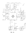
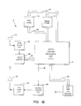
- Figs. 1Aand 1B are block diagrams of the present invention.
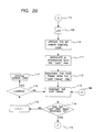
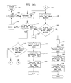
- Figs. 2A-2E are flow charts for the transmission process of the first embodiment of the present invention.
- Fig. 3 illustrates how data is modulated in the first embodiment of the present invention.
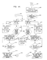
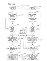
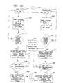
- Figs. 4A-4C are flow charts for the reception process of the first embodiment of the present invention.
- Figs. 5A-5C are block diagrams of the various system configurations for the various embodiments of the present invention.
- the packet communications system for the first embodiment of the present invention utilizes a transmitter control system 1 to transmit data to a receiver.
- the transmitter control system 1 of the present invention is illustrated in Fig. 1A.
- the central processing unit (CPU) 3 is the main controller for the transmitter control system 1 and includes the necessary read only memory (ROM) random access memory (RAM) necessary, and clock signals for its operation.
- ROM read only memory
- RAM random access memory
- An address bus 33 is used to allow the CPU 3 to access a specific portion of a particular circuit attached thereto. Part of the address bus 33 is used to specify the particular circuit, another part of the address bus 33 is used to access a specific portion of the particular circuit.
- the address bus also contains a write enable signal which allows the storage of information into the specific portion of the particular circuit from the data bus 35 when the write enable signal is asserted. When the write enable signal is not asserted, information from the specific area of the particular circuit addressed is transferred to the CPU 3 on the data bus 35.
- the transfer of data to and from storage circuitry as described above is well-known in the microprocessor art.
- the frame store 9 is used to store the packets of information as frames of bits in the first embodiment.
- the pseudo-random number (PRN) store 11 is used to store the various pseudo-random numbers used in the first embodiment to modulate each frame of data to be transmitted.
- the digital modulation circuit 19 is used to modulate the bit frame or portion thereof provided to it by CPU 3 on the BF data line by the portion of a PRN provided to it by the CPU 3 on the data bus 35. Once the digital modulation circuit 19 is accessed by the address bus 35, and the ENABLE line is activated by the CPU 3, the data on the BF data line is modulated and the result thereof is produced on the CF data line representing the chip frame data for that portion of the bit frame just modulated.
- the bit frames are stored in the output buffer circuit 13 as they are modulated.
- the transmitter control circuit 15 accesses the output buffer 13 to retrieve data to be transmitted.
- the transmitter control circuit utilizes and address bus 37 to access storage locations within the output buffer 13 so as to retrieve data on the data bus 39.
- the address busses 37 and 35 are connected to circuitry within the output buffer 13 so that only one data bus can access the output buffer memory during any one portion of a clock cycle.
- Transmitter control circuit 15 transmits the modulated bit frames along a data path of a communications channel via antenna 17.
- the antenna 29 is used to receive the CRA signal along a feedback path of the communications channel which is sent by the receiver.
- An input buffer circuit 25 is used to store each chip of the CRAas it is received from the CRAdetec- tion circuit 27.
- Data line 25 is connected to dedicated input ports of the CPU 3 so as to transmit the CRA chips stored in the input buffer circuit 25 when they are received by the input buffer circuit 25.
- Other dedicated ports include the BF data line, the CF data, the ENABLE line, and the data bus 41.
- Block 101 is the start of the transmission process which may be initiated in any conventional manner, e.g., pushing a transmit button.
- Block 102 is performed after the transmission process begins and until at least one packet has been stored within the input buffer circuit 9.
- the input buffer circuit 9 is provided with data from an external input peripheral device 21.
- the data stored in the input buffer circuit 9 are the bits which make up each packet. Once it is determined that a packet of information is available within the input buffer circuit 19, then a packet is retrieved therefrom as illustrated in block 103. In the first embodiment I will assume that the packet consists of 1384 bits.
- the packet retrieved from the input buffer circuit 19 may fit one of four categories; a First Packet, an Even Packet, an Odd Packet, or a Last Packet. It is possible for a special case to occur where only one packet is in the input buffer in which case it will be treated as a Last Packet (even though it is also a First Packet). Of these four possible cases, only two are possible options at any given time based on the type of packet that preceded it, and of the two possible options one of the options is always the Last Packet option. For example, if the first packet has been retrieved, then that packet could be a first packet or a last packet. If the packet retrieved is the second packet, then the packet is either an even packet or a last packet. If the packet retrieved is the third packet retrieved since the "yes" decision was made in block 102, then the packet is an odd packet or a last packet, etc.
- step 105 is to set a counter F to zero for purposes described below.
- an error control code is added to the packet to produce a frame as indicated by step 106.
- This bit level error control code will be used by the receive station to determine the validity of the received frame of information.
- many such codes exist in the prior art such as the CRC-16, or CRC-CCITT.
- CRC-16 or CRC-CCITT.
- 16 bits are used by the error control code.
- the combination of 1384 bits in the packet with 16 error control bits yields a frame of 1400 bits.
- the spread spectrum modulation and interleaving process is accomplished. This is the process by which the random burst component of the compound error channel is effectively purged from the system by distributing its energy over the frame.
- the preferred method of spread spectrum modulation and interleaving is conducted as follows for the first chip frame:
- the digital modulation circuit 19 is used to modulate the bit frame to generate the chip frame.
- Figure 3 illustrates a block diagram of a portion of the modulation circuit 19.
- Bit frame data from the BF data line are stored in frame bit locations 1 through Y of memory 50, where Y is equal to 1,400 in the first embodiment. For example, if the BF data line is connected to 16 dedicated ports of the CPU 3 and the digital modulation circuit, then the BF data line would have to be loaded 88 times to completely store all 1,400 bits of the frame, wherein during the eighty-eighth time only half of the BF data is left.
- the PRN data is loaded into chip generators 51 from the data bus 35 in the same manner as the memory circuits 50 are loaded. Both memory circuits 50 and chip generator circuits 51 are accessed by the address bus 33 so that the bit frame data and PRN data are stored at the same time.
- the chip generator circuits 51 have storage locations to store the PRN bits and also have exclusive or (XOR) logic circuitry to produce an output upon receiving the ENABLE signal so as to XOR each bit frame with the appropriate chip frame as discussed above, thereby producing the modulated bit frame as the chip frame data.
- the chip frame data is stored in memory circuits 52. If the CF data line has 16 dedicated ports connecting the digital modulation circuit 19 and the CPU 3, then the address bus will have to access the chip frame eighty-eight times, wherein during the eighty-eighth time only half of the memory circuits 51 are accessed, e.i. only eight bits of information would be transferred to the CPU 3.
- the order of the chips is scrambled in accordance with a "chip frame" PRN.
- the first chip may be located in the eighth chip location or some other location.
- the objective here is similar to that in step 107 except this step is specifically designed to counter burst noise that is in synchronization with the chip frame structure (that is jamming).
- This is the process by which the cyclic synchronized burst component of the compound error channel is effectively purged from the system by distributing its energy overthe frame. For example, if the synchronized burst component tends to occur in the eighth chip frame component, then for the first frame the first chip may be lost since it was changed to the eighth chip location. In a subsequent chip frame the eighth chip location would be occupied by another chip representing a different bit of the frame.
- a method of visualizing this would be to think of it as a Time Division Multiplexed channel with 1400 assigned time slots. Each time slot would contain one chip representing the bit frame after it has been modulated. This is done 1000 times.
- the transmitter control circuit 15 begins to transmit the first chip frame, see block 28 of Fig. 2C, and then the CPU 3 waits to receive the first CRA signal from the receiver, see block 129.
- steps 132 and 133 the number of chip frames transmitted are counted and, if they exceed 1000 for the first frame, a malfunction has occurred in the system. A system error is indicated to the operator if this occurs, see block 34.
- the receiver control system 2 to be described later, would be able to demodulate the chip frames representing the first frame before the one-thousandth chip frame is transmitted unless a hardware failure occurs.
- the CPU 3 While the transmission process represented in blocks 128, 129, 132, and 133 are being performed by the transmit control circuitry 15, the CPU 3 is retrieving the next packet to be transmitted, see block 118. In block 119, the next step is to determine whether this packet is the last packet. If not, then the second packet is to be transmitted. The counter E is set to zero in block 121.
- the steps performed in blocks 123, 125, and 127 perform the same function on the second frame or any subsequent even frame as the steps which were performed on the first frame in blocks 16,17, and 18, respectively. If the second packet, or any subsequent even packet, happens to be the last packet to be transmitted, the steps in blocks 120, 122, 124, and 129 are performed which are identical to the steps performed in blocks 121, 123, 125, and 127 for an even packet. After the next packet to be transmitted is modified to a bit frame as discussed above and that bit frame is modulated to be a series of chip frames as discussed above, then the CPU 3, waits for the reception for the first CRA signal, see block 129.
- the system 2 transmits the first CRA along the feedback path of the communications channel, see Fig. 5A.
- the first CRA has been received as determined in block 129 of Fig. 2C, it is determined whether or not the packet just modulated by the CPU 3 as discussed above while the first chip frame was being transmitted is the last packet. If not, then the process goes on to the steps in Fig. 2D. Note that steps 118 through 127 are a parallel process performed simultaneously with steps 128, 129, 132, and 133.
- Fig. 2D is identical to Fig. 2C except that the packet modulated in the steps of blocks 140-144 is an odd packet, such as the third packet after the yes decision of block 102 in Fig. 2A. Also, in step 146 the transmitter system is waiting for an even CRA since the current chip frames being transmitted represent the bit frame of the second packet or some other even packet retrieved from the input buffer circuit 9 since the last yes decision of block 102.
- the next step is to determine whether or not the previous packet modulated in the parallel process of Fig. 2E, e.g., blocks 152, 153, etc., was the last packet to be retrieved in the input buffer circuit 9. If not the process goes back to the procedures of Fig. 2D.
- the processes of Figs. 2D and 2E are performed until a last packet is retrieved. Note that any packet which is not even, not the first packet, and not the last packet, is considered odd although it may be the thirteenth packet or some other prime number packet.
- Blocks 113, 114, 114, and 116 perform the same steps as blocks 128, 129, 132, and 133 did for the first packet transmitted. Note that blocks 109 through 112 are performed only if the first packet is also the last packet to be transmitted. Once the last CRA is received as determined in block 114, the process returns to step 102 to wait for the next available packet.
- the reception process consists of some preliminary steps required for synchronization that are in continuous operation, see blocks 201, 202, and 203.
- the step represented in block 204 correlates the first bit frame (FBF). This process is simply inverting the actions performed by the transmitter.
- the synchronization process gives the exact time to commence the process, and the pseudo random structures to rearrange the chip frames back to the bit frame order is known, and the exact duration of the chip frame is provided by the synchronization process so the process of associating the chips for given bit is clear and the pseudo random sequence used to modulate the bits is a known factor.
- the receiver control system 2 is shown in Fig. 1 B.
- the antenna 16 receives the transmitted data from the data path.
- the data signal is detected by the data receiver circuit 18 and is and the received chip data is input to the input buffer 20.
- the data line 40 transfers data from the input buffer 20 to the CPU 4 of the receiver.
- PRN store 10 stores the same PRNs which are identical to the PRNs stored in the transmitter controller system 1. In this manner the location of each chip representing a particular bit frame location can be determined as well as the particular PRN bit which modulated that particular bit of the frame. Since the XOR technique was used to modulate the bits of the frame, then if the bit of the PRN agrees with the received chip, than the demodulated bit would be a zero; otherwise, the modulated bit was a one.
- the receiver With synchronization achieved, the receiver knows exactly which PRN modulated which bit of the frame, and is therefore able to modulate each chip to reconstruct the bit frame as each chip frame is received. However, it is to be noted that some of the chip frames are going to be corrupted by noise so as to be improperly demodulated. After enough of the chip frames are received, eventually a majority of the chips will indicate the proper bit modulated, while a minority of the chips were chips which were improperly demodulated.
- the step performed in block 206 establishes some basic threshold requirements to exceed before an attempt to generate the bit frame is made.
- the first requirement is that the current chip to bit ratio (CBR) at the receiver for this bit frame be greater than the chip to bit ratio required to overcome the known thermal noise for the communications channel. Reliable communications can not occur below this value. Any "valid" bit frames below this value are a result of small sample size statistical odds and are likely to be a false "valid" indication.
- the second requirement is that the CBR must be greater than 80% of the equivalent value associated with the synchronization signal (0.8R). For example, if 80% of the chips of the synchronization signal sent by the transmitter are received correctly, then at least 64% of the chips received for each bit of the frame must agree that chip is a particular binary digit. After each chip frame is received, and the preliminary conditions are meet, a chip frame is calculated.
- bit frame error control code is evaluated to determine frame validity. If the frame is not valid, another chip frame is added to the correlation by cycling back through steps 204 & 206. If the bit frame is validated the correlation buffers are reset in preparation for the next bit frame (step 16), and the acknowledgment process is started (step 10).
- step 212 does require clarification.
- the receiver "knows" what the transmitter is sending in both structure and content. Given this fact the chip stream can be compared to one generated by the receiver to detect when the transition to the next bit frame has occurred. The reason why separate First, Last, Even & Odd codes are used if to ensure that the transitions will be identified. It is possible that if a series of packets are being transmitted, and a burst of noise occurred such that the receiving station never recognized the transitions to the next frame and continues sending the CRA, the continuous CRA could be used for the wrong packet by the transmitter.
- time/distance factors those being the distance between the transmitter and receiver, the chip transmission rate, the nominal chip to bit ratio, and the number of bits in the frame need to be chosen carefully for optimum performance.
- the method of obtaining a high energy efficiency is by the careful selection of the nominal chip-to-bit ratio (usually greater than 99 to achieve a nominal throughput efficiency of 99% or better), frame size (greater than three times the nominal chip-to-bit ratio plus two "processing" times), and the physical distance separating station "A" from station “B” over the channel.
- the requirement is that station “B” must determine that a "valid” packet of data has been received and station "A” must "know” this fact in less time than is required for station :"A" to transmit one chip frame.
- station B will validate the proper reception of a frame of information after receiving 100 chip frames the following sequence of events and time intervals illustrates the proper time/distance relationships.
- a feedback path is used for the CRA signal while the data path is used to transmit the chip frames as well as a synchronization signal as discussed above.
- the feedback path of the communications channel can be omitted.
- the second embodiment is a full duplex system in which a transmitter control system 1Aand a receiver control system 2A are located at a site A, while receiver control system 2B and transmitter control system 1 B are located at a different site B.
- the transmitter control systems 1A and 1 B have the same circuit diagram as transmitter control system 1 as illustrated in Fig. 1A.
- the transmitter control system 1A transmits the chip frames and a synchronization signal along the data path AB.
- the synchronization signal also contains the CRA signal which will be explained in more detail below.
- the receiver control system 2B receives the chips in the same manner as the receiver controls system 2 does. The only difference is that the receiver 2B also receives the CRA signal and must decode it. This is not a problem since, as discussed above, there are only two alternative CRA signals which the receiver looks for at any one time, dependent on the previous frame received.
- the receiver is either looking for a first CRA signal to be transmitted along with the synchronization signal or last CRAsignal to be transmitted along with the synchronization signal. If only the synchronization signal is received by the receiver control system 2B, then the receiver control system 2A has not yet decoded the chip frame being presently transmitted by the transmitter control system 1 B. If the receiver control system 2A had decoded the chip frame being transmitted by the transmitter control system 1 B, then the receiver control system 2A would indicate this to the transmitter control system 1Avia an external peripheral output device 30 connected to one of the external peripheral input devices 21 of the transmitter control system 1A.
- the transmitter control system 1A transmits the proper CRA signal along the data path AB along with the synchronization signal and the chip frame being transmitted by the transmit- tercontrol system 1A.
- the receiver control system 2B would then indicate to the transmitter control system 1 B that the receiver control system 2A has decoded the present bit frame.
- the transmitter control system stops transmitting the chip frames of that bit frame in the same manner as disclosed with the first embodiment.
- the transmitter control system 1 B starts transmitting at this point the next series of chip frames representing the next bit frame to be transmitted.
- receiver control system 2B properly demodulates the bit frame being transmitted by the transmitter control system 1A, then the receiver control system indicates this to the transmitter control system 1 B, which in turn indicates this to the receiver control system 2A, which in turn informs the transmitter control system 1A. This is accomplished in the same manner that the receiver control system 2A informed the transmitter control system 1B described above. In this manner, in the second embodiment of the present invention, separate feedback paths are not required.
- the transmitter control system 1 C has the same circuit configuration as the transmitter control system loft he first embodiment.
- the receiver control system 2C has the same circuitry configuration as receiver control system 2 of the first embodiment.
- the transmitter control system 1 C takes the data input to it and modulates it to create the interleaves chip frames as discussed above, e.g. see the discussion of block 107 of Fig. 2A. Also, if desired, the positioning of the chip frame locations may be rearranged as discussed above, e.g. see the discussion of block 108 of Fig 2A.
- the receiver control system 2C demodulates the data on the data path in the same manner as discussed above in conjunction with the first embodiment; however, no CRA is sent.
- the data input to the transmitter control system 1 C could be packets of information discussed above, or it could be chip frames which are not interleaved, i.e. all chips in one contiguous group represent one bit of the frame.
- the transmitter control system 1 would simply store the entire chip frame and transmit it in an interleaved fashion as discussed above so as to transform a compound error communications path to a gaussian noise channel by spreading any burst noise which may occur in a contiguous stream of chips among many modulated bit frames since each contiguous chip represents a different bit frame.
Landscapes
- Engineering & Computer Science (AREA)
- Computer Networks & Wireless Communication (AREA)
- Signal Processing (AREA)
- Detection And Prevention Of Errors In Transmission (AREA)
- Communication Control (AREA)
- Noise Elimination (AREA)
Applications Claiming Priority (2)
| Application Number | Priority Date | Filing Date | Title |
|---|---|---|---|
| US965700 | 1992-10-23 | ||
| US07/965,700 US5274667A (en) | 1992-10-23 | 1992-10-23 | Adaptive data rate packet communications system |
Publications (2)
| Publication Number | Publication Date |
|---|---|
| EP0594325A2 true EP0594325A2 (fr) | 1994-04-27 |
| EP0594325A3 EP0594325A3 (fr) | 1995-02-08 |
Family
ID=25510361
Family Applications (1)
| Application Number | Title | Priority Date | Filing Date |
|---|---|---|---|
| EP93307950A Withdrawn EP0594325A3 (fr) | 1992-10-23 | 1993-10-06 | Système de communication de paquets avec taux de transmission de données adaptatif. |
Country Status (4)
| Country | Link |
|---|---|
| US (2) | US5274667A (fr) |
| EP (1) | EP0594325A3 (fr) |
| JP (1) | JPH06204987A (fr) |
| CA (1) | CA2103744A1 (fr) |
Cited By (1)
| Publication number | Priority date | Publication date | Assignee | Title |
|---|---|---|---|---|
| WO1995010145A1 (fr) * | 1993-10-04 | 1995-04-13 | Nokia Telecommunications Oy | Procede d'amelioration de la qualite de signaux par ajustage du rapport d'etalement dans un systeme cellulaire de radiotelephonie de type amdc |
Families Citing this family (28)
| Publication number | Priority date | Publication date | Assignee | Title |
|---|---|---|---|---|
| US8352400B2 (en) | 1991-12-23 | 2013-01-08 | Hoffberg Steven M | Adaptive pattern recognition based controller apparatus and method and human-factored interface therefore |
| US10361802B1 (en) | 1999-02-01 | 2019-07-23 | Blanding Hovenweep, Llc | Adaptive pattern recognition based control system and method |
| US5274667A (en) * | 1992-10-23 | 1993-12-28 | David Olmstead | Adaptive data rate packet communications system |
| US5420593A (en) * | 1993-04-09 | 1995-05-30 | Trimble Navigation Limited | Method and apparatus for accelerating code correlation searches in initial acquisition and doppler and code phase in re-acquisition of GPS satellite signals |
| TW306102B (fr) * | 1993-06-14 | 1997-05-21 | Ericsson Telefon Ab L M | |
| US5363404A (en) * | 1993-07-13 | 1994-11-08 | Motorola Inc. | Apparatus and method for conveying information in a communication network |
| CA2145566C (fr) * | 1994-04-29 | 1999-12-28 | Nambirajan Seshadri | Methodes et dispositifs pour ameliorer les communications a etalement du spectre |
| JP2737655B2 (ja) * | 1994-07-12 | 1998-04-08 | 双葉電子工業株式会社 | スペクトル拡散通信方式 |
| US5883899A (en) * | 1995-05-01 | 1999-03-16 | Telefonaktiebolaget Lm Ericsson | Code-rate increased compressed mode DS-CDMA systems and methods |
| US5896368A (en) * | 1995-05-01 | 1999-04-20 | Telefonaktiebolaget Lm Ericsson | Multi-code compressed mode DS-CDMA systems and methods |
| US6252898B1 (en) * | 1995-07-19 | 2001-06-26 | Hitachi Denshi Kabushiki Kaisha | Spread spectrum communication method and system wherein data rate of data to be transmitted is changed in accordance with transmission quality |
| US5737357A (en) * | 1995-09-08 | 1998-04-07 | Motorola, Inc. | Apparatus and method for data pattern sensitivity correction |
| JPH09321659A (ja) * | 1996-05-31 | 1997-12-12 | Fujitsu Ltd | スペクトラム拡散通信方式 |
| US6061386A (en) * | 1997-03-19 | 2000-05-09 | I.C. Com Ltd. | Method of chip interleaving in direct sequence spread spectrum communications |
| US6301288B1 (en) | 1997-03-19 | 2001-10-09 | Infineon Technologies Ag | Method of chip interleaving in direct sequence spread spectrum communications |
| US6046991A (en) * | 1997-04-09 | 2000-04-04 | Aloha Networks, Inc. | TDM variable broadcast energy transmitter |
| SE511561C2 (sv) * | 1997-05-02 | 1999-10-18 | Ericsson Telefon Ab L M | Anordningar och förfarande relaterande till hantering av digitala signaler |
| US7268700B1 (en) | 1998-01-27 | 2007-09-11 | Hoffberg Steven M | Mobile communication device |
| US6067646A (en) * | 1998-04-17 | 2000-05-23 | Ameritech Corporation | Method and system for adaptive interleaving |
| EP0975118B1 (fr) | 1998-07-24 | 2007-05-09 | Matsushita Electric Industrial Co., Ltd. | Système et procédé de communication radio à AMRC |
| US7966078B2 (en) | 1999-02-01 | 2011-06-21 | Steven Hoffberg | Network media appliance system and method |
| US6493405B1 (en) | 1999-03-02 | 2002-12-10 | Harris Corporation | Correlator having enhanced memory for reference and input data |
| US6438182B1 (en) | 1999-03-02 | 2002-08-20 | Harris Corporation | Correlator with serial-parallel partition |
| US6038271A (en) * | 1999-03-02 | 2000-03-14 | Harris Corporation | Correlator with cascade data paths to facilitate expansion of correlator length |
| JP3595738B2 (ja) | 1999-08-30 | 2004-12-02 | 松下電器産業株式会社 | 距離検出方法、位置検出方法及びその装置 |
| US7620154B2 (en) | 2002-12-23 | 2009-11-17 | Cambron G Keith | Equivalent working length determinative system for digital subscriber line circuits |
| US9818136B1 (en) | 2003-02-05 | 2017-11-14 | Steven M. Hoffberg | System and method for determining contingent relevance |
| US7515541B2 (en) * | 2003-08-08 | 2009-04-07 | Intel Corporation | Transmission of data with feedback to the transmitter in a wireless local area network or the like |
Family Cites Families (15)
| Publication number | Priority date | Publication date | Assignee | Title |
|---|---|---|---|---|
| US3754211A (en) * | 1971-12-30 | 1973-08-21 | Ibm | Fast error recovery communication controller |
| JPS5573157A (en) * | 1978-11-27 | 1980-06-02 | Ricoh Co Ltd | Data communication system |
| US4418393A (en) * | 1980-10-27 | 1983-11-29 | Sperry Corporation | Matched filter spread spectrum code recovery apparatus |
| US4393501A (en) * | 1981-02-26 | 1983-07-12 | General Electric Company | Line protocol for communication system |
| DE3304300A1 (de) * | 1983-02-09 | 1984-08-09 | Brown, Boveri & Cie Ag, 6800 Mannheim | Verfahren und einrichtung zur busanforderung und sammelquittierung in einem prozessbus-system |
| US4761796A (en) * | 1985-01-24 | 1988-08-02 | Itt Defense Communications | High frequency spread spectrum communication system terminal |
| FR2595522A1 (fr) * | 1986-03-06 | 1987-09-11 | Cimsa Sintra | Procede et dispositif de transmission de donnees numeriques par messages organises en trames |
| US4694467A (en) * | 1986-07-03 | 1987-09-15 | Signatron, Inc. | Modem for use in multipath communication systems |
| US4905234A (en) * | 1987-06-03 | 1990-02-27 | General Electric Company | Apparatus and method for transmitting digital data over a radio communications channel |
| US5067136A (en) * | 1988-11-02 | 1991-11-19 | Axonn Corporation | Wireless alarm system |
| US5016255A (en) * | 1989-08-07 | 1991-05-14 | Omnipoint Data Company, Incorporated | Asymmetric spread spectrum correlator |
| US5128958A (en) * | 1990-07-26 | 1992-07-07 | Unisys Corp. | Digital time error signal generator |
| US5157688A (en) * | 1991-03-14 | 1992-10-20 | Hughes Aircraft Company | Spread spectrum transmitter for degrading spread spectrum feature detectors |
| US5159608A (en) * | 1991-08-28 | 1992-10-27 | Falconer David D | Method and apparatus for using orthogonal coding in a communication system |
| US5274667A (en) * | 1992-10-23 | 1993-12-28 | David Olmstead | Adaptive data rate packet communications system |
-
1992
- 1992-10-23 US US07/965,700 patent/US5274667A/en not_active Expired - Fee Related
-
1993
- 1993-08-10 CA CA002103744A patent/CA2103744A1/fr not_active Abandoned
- 1993-08-27 US US08/112,321 patent/US5335247A/en not_active Expired - Fee Related
- 1993-10-06 EP EP93307950A patent/EP0594325A3/fr not_active Withdrawn
- 1993-10-22 JP JP5265218A patent/JPH06204987A/ja active Pending
Cited By (1)
| Publication number | Priority date | Publication date | Assignee | Title |
|---|---|---|---|---|
| WO1995010145A1 (fr) * | 1993-10-04 | 1995-04-13 | Nokia Telecommunications Oy | Procede d'amelioration de la qualite de signaux par ajustage du rapport d'etalement dans un systeme cellulaire de radiotelephonie de type amdc |
Also Published As
| Publication number | Publication date |
|---|---|
| US5274667A (en) | 1993-12-28 |
| CA2103744A1 (fr) | 1994-04-24 |
| JPH06204987A (ja) | 1994-07-22 |
| EP0594325A3 (fr) | 1995-02-08 |
| US5335247A (en) | 1994-08-02 |
Similar Documents
| Publication | Publication Date | Title |
|---|---|---|
| US5274667A (en) | Adaptive data rate packet communications system | |
| US4649543A (en) | Synchronization sequence decoder for a digital radiotelephone system | |
| US6606313B1 (en) | Random access in a mobile telecommunications system | |
| US5434847A (en) | Random access satellite communication system using random numbers generated in a range variable with channel traffic | |
| Abramson | The ALOHA system: Another alternative for computer communications | |
| US4736371A (en) | Satellite communications system with random multiple access and time slot reservation | |
| US4517679A (en) | Communication over noisy lines | |
| US5404374A (en) | Method and apparatus for transmitting and receiving encoded data using multiple frequency coding | |
| US4532635A (en) | System and method employing two hop spread spectrum signal transmissions between small earth stations via a satellite and a large earth station and structure and method for synchronizing such transmissions | |
| US4761778A (en) | Coder-packetizer for random accessing in digital communication with multiple accessing | |
| EP1244239A2 (fr) | Procédé et dispositif de codage et de transmission de données sur un support bruité | |
| EP2417722B1 (fr) | Contrôle dynamique de puissance | |
| US3879577A (en) | Data transmission system | |
| EP1988658A2 (fr) | Retransmission automatique dont l'ordre d'informations est modifié | |
| RU2002116668A (ru) | Устройство и способ гибридного запроса автоматического повторения для системы мобильной связи | |
| CA1259659A (fr) | Systeme radiotelephonique utilisant la signalisation par donnees vocales numerisees | |
| Pursley et al. | Incremental-redundancy transmission for meteor-burst communications | |
| US5657342A (en) | Adaptive data rate packet communication system | |
| US5313473A (en) | Method and apparatus for digital data transmission with automatic repeat request | |
| US5483545A (en) | Method of automatically requesting retransmission in a duplex digital transmission system having at least one noisy return channel, and an installation for implementing the method | |
| MXPA06010313A (es) | Canal de acceso con tiempos de llegada restringidos. | |
| US5333197A (en) | System to prevent a scrambler from generating undesired symbols | |
| JP2530603B2 (ja) | バケツトデ−タ受信装置 | |
| EP1075744B1 (fr) | Systeme de transmission de donnees avec demande de repetition automatique | |
| CA2215380C (fr) | Procede et dispositif de codage et de transmission de donnees via un support bruyant |
Legal Events
| Date | Code | Title | Description |
|---|---|---|---|
| PUAI | Public reference made under article 153(3) epc to a published international application that has entered the european phase |
Free format text: ORIGINAL CODE: 0009012 |
|
| AK | Designated contracting states |
Kind code of ref document: A2 Designated state(s): AT BE CH DE DK ES FR GB GR IE IT LI LU MC NL PT SE |
|
| PUAL | Search report despatched |
Free format text: ORIGINAL CODE: 0009013 |
|
| AK | Designated contracting states |
Kind code of ref document: A3 Designated state(s): AT BE CH DE DK ES FR GB GR IE IT LI LU MC NL PT SE |
|
| 17P | Request for examination filed |
Effective date: 19950731 |
|
| 18D | Application deemed to be withdrawn |
Effective date: 19980501 |