EP0594328A1 - Methode zur Steuerung von Plasmaverfahren - Google Patents
Methode zur Steuerung von Plasmaverfahren Download PDFInfo
- Publication number
- EP0594328A1 EP0594328A1 EP93307962A EP93307962A EP0594328A1 EP 0594328 A1 EP0594328 A1 EP 0594328A1 EP 93307962 A EP93307962 A EP 93307962A EP 93307962 A EP93307962 A EP 93307962A EP 0594328 A1 EP0594328 A1 EP 0594328A1
- Authority
- EP
- European Patent Office
- Prior art keywords
- gas
- plasma
- chamber
- pressure
- temperature
- Prior art date
- Legal status (The legal status is an assumption and is not a legal conclusion. Google has not performed a legal analysis and makes no representation as to the accuracy of the status listed.)
- Granted
Links
Images



Classifications
-
- H—ELECTRICITY
- H01—ELECTRIC ELEMENTS
- H01J—ELECTRIC DISCHARGE TUBES OR DISCHARGE LAMPS
- H01J37/00—Discharge tubes with provision for introducing objects or material to be exposed to the discharge, e.g. for the purpose of examination or processing thereof
- H01J37/32—Gas-filled discharge tubes
- H01J37/32431—Constructional details of the reactor
- H01J37/3244—Gas supply means
- H01J37/32449—Gas control, e.g. control of the gas flow
-
- H—ELECTRICITY
- H01—ELECTRIC ELEMENTS
- H01J—ELECTRIC DISCHARGE TUBES OR DISCHARGE LAMPS
- H01J37/00—Discharge tubes with provision for introducing objects or material to be exposed to the discharge, e.g. for the purpose of examination or processing thereof
- H01J37/32—Gas-filled discharge tubes
- H01J37/32009—Arrangements for generation of plasma specially adapted for examination or treatment of objects, e.g. plasma sources
- H01J37/32192—Microwave generated discharge
-
- H—ELECTRICITY
- H01—ELECTRIC ELEMENTS
- H01J—ELECTRIC DISCHARGE TUBES OR DISCHARGE LAMPS
- H01J37/00—Discharge tubes with provision for introducing objects or material to be exposed to the discharge, e.g. for the purpose of examination or processing thereof
- H01J37/32—Gas-filled discharge tubes
- H01J37/32431—Constructional details of the reactor
- H01J37/3244—Gas supply means
-
- H—ELECTRICITY
- H01—ELECTRIC ELEMENTS
- H01J—ELECTRIC DISCHARGE TUBES OR DISCHARGE LAMPS
- H01J37/00—Discharge tubes with provision for introducing objects or material to be exposed to the discharge, e.g. for the purpose of examination or processing thereof
- H01J37/32—Gas-filled discharge tubes
- H01J37/32431—Constructional details of the reactor
- H01J37/3266—Magnetic control means
- H01J37/32678—Electron cyclotron resonance
-
- H—ELECTRICITY
- H01—ELECTRIC ELEMENTS
- H01J—ELECTRIC DISCHARGE TUBES OR DISCHARGE LAMPS
- H01J37/00—Discharge tubes with provision for introducing objects or material to be exposed to the discharge, e.g. for the purpose of examination or processing thereof
- H01J37/32—Gas-filled discharge tubes
- H01J37/32917—Plasma diagnostics
- H01J37/3299—Feedback systems
-
- Y—GENERAL TAGGING OF NEW TECHNOLOGICAL DEVELOPMENTS; GENERAL TAGGING OF CROSS-SECTIONAL TECHNOLOGIES SPANNING OVER SEVERAL SECTIONS OF THE IPC; TECHNICAL SUBJECTS COVERED BY FORMER USPC CROSS-REFERENCE ART COLLECTIONS [XRACs] AND DIGESTS
- Y10—TECHNICAL SUBJECTS COVERED BY FORMER USPC
- Y10S—TECHNICAL SUBJECTS COVERED BY FORMER USPC CROSS-REFERENCE ART COLLECTIONS [XRACs] AND DIGESTS
- Y10S438/00—Semiconductor device manufacturing: process
- Y10S438/935—Gas flow control
Definitions
- the present invention relates to methods for controlling plasma processes of the type used in the microelectronics industry for the etching, deposition and cleaning of thin films.
- Plasma processes have become important in the manufacture of semiconductor devices such as integrated circuits.
- Low pressure glow discharge plasmas are used in the anisotropic etching of fine-line patterns, and plasmas are routinely used for low temperature deposition of insulating and passivating layers such as silicon nitride.
- Typical plasma reactors for microelectronics applications comprise a low pressure chamber, a source of gas to be converted to plasma, and a source of energy to convert the gas to plasma.
- new plasma generators are those based on electron cyclotron resonance heating.
- microwaves from an external source are launched through a dielectric window into the chamber to excite the gas within the chamber and thus create a plasma.
- Such generators permit separate control of plasma generation and ion transport.
- ion flux and ion energy can be controlled separately to optimize throughput, selectivity and anisotropy while minimizing ion-induced atomic displacement damage.
- plasmas are not well understood and their behavior can fluctuate in seemingly random ways which can greatly affect their useful properties. Specifically, by virtue of their non-linear properties, plasmas are prone to instability, bistability, and hysteresis which can deteriorate the reproducibility of critical semiconductor manufacturing processes. Present control schemes based on maintaining constant pressure have not been adequate to prevent serious fluctuations in etch rate and deposition rate in plasma-based semiconductor manufacturing processes.
- a plasma generated within a plasma confinement chamber for use in manufacturing semiconductor devices is controlled by monitoring both the neutral gas pressure P and the neutral gas temperature T.
- the process parameters P and T are then adjusted to control P/T n .
- the pressure is adjusted to maintain P/T constant by adjusting the gas flow rate or the outlet pumping speed. The result is a plasma exhibiting enhanced stability over prolonged periods of time.
- FIG. 1 is a graphical illustration useful in understanding the problem to which the present invention is directed.
- FIG. 1 is a plot of the floating potential versus pressure at temperature equilibrium for a representative ECR generator. With each pressure increment the reactor is given a period of about 60 s to achieve equilibrium before the potential is measured. As can be seen, the potential exhibits sharp transitions at pressures of about 1 m Torr and at about 3.0 m Torr. In particular, the bistability at 1 m Torr is sufficiently large that it can alter the ion flux to device wafers by more than a factor of two. Moreover, if the pressure is changed slowly, a hysteresis can be observed and the transition pressure will depend on the direction of pressure change.
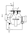
- FIG. 3 is a schematic illustration of a typical plasma generating apparatus adapted for P/T n control.
- the FIG. 3 apparatus is a conventional ECR plasma reactor modified by the presence of a temperature probe 1 to provide a measure of the temperature T of the plasma and a system controller 2 responsive to P and T to control P/T n .
- This control is conveniently effected by varying the gas pressure in such a fashion as to maintain P/T n substantially constant.
- the controller is adapted to vary the gas pressure so that P/T is maintained at values removed at least 5% (in either direction) from values of P/T which exhibit plasma instability.
- the plasma reactor 10 can be a conventional ECR reactor comprising a low pressure chamber 20 including a quartz window 21, a quartz plasma liner 22 and an electrode 23 for supporting a workpiece (not shown) to be plasma processed as by etching or deposition.
- the chamber 20 is provided with gas entry aperture 24 for permitting introduction of neutral gas and a gas exit aperture 25 for removing gas and plasma products.
- the plasma generating apparatus comprises a microwave source 30 and an electromagnet 31.
- the source 30 launches through window 21 microwaves at the electron cyclotron resonance frequency determined by the field of electromagnet 31.
- Liner 22 is designed to conform to the shape of the magnetic field lines in order to avoid sputtering of the chamber walls by the plasma.
- the system control arrangement comprises a gas inlet controller 40 for controlling the rate of gas flow into chamber 20, an outlet controller 41 for controlling the rate at which gas and plasma products are removed from the chamber by pump 42, a pressure sensor43 for measuring the pressure P in chamber 20 and a temperature probe 1 to provide a measure of the temperature T in the plasma.
- temperature probe 1 is disposed on a back wall protected by liner 22 from the plasma. Sensor 43 and probe 1 provide to system controller 2 signals indicative of P and T, and controller 2, in turn, provides control signals to inlet controller 40 and outlet controller 41 in order to maintain P/T n substantially constant.
- gas introduced into the chamber 20 through aperture 24 is ionized by microwave ECR heating.
- the plasma is contained by the field from magnet 31 while the chamber wall is protected by liner 22.
- Ions for plasma processing are drawn toward a workpiece on electrode 23 by application of a suitable bias to the electrode.
- P and T are measured, and the pressure P is varied in proportion to T " so that P/T n is constant.
- P is maintained proportional to the first power of T by adjusting the inlet flow rate and/or the outlet pumping speed.
- the pressure is preferred to adjust the pressure by adjusting the flow rate so that the mean gas residence time remains substantially constant.
- T is to be measured by an absolute scale. It is also to be understood that T can be measured from any material in thermal equilibrium with the gas.
- generating apparatus 10 can comprise an Astex S-1500 ECR source.
- Gas inlet controller40 can be an MKS Multigas 147 Controller and outlet controller 41 can be a VAT PM-5 adaptive pressure controller.
- this apparatus pump 42 can be a Balzers TCP 5000, pressure sensor 43 a MKS 390 HA and temperature probe 1 an Omega Type E thermocouple.
- Typical process operating parameters are as follows:
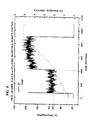
- FIGS. 4 and 5 are graphical illustrations useful in showing the improvement in plasma stability effected by P/T control.
- FIG. 4 is a plot of floating potential (and temperature) versus time in a simulated manufacturing process sequence wherein the microwave input power is gated on for 60s then off for 30s. The plasma on- time corresponds to process time while the off-time corresponds to the time needed to remove the processed wafer from the chamber and install the next wafer to be processed.
- FIG. 4 shows the process where pressure alone is maintained constant. Significantly, temperature increases and instability is encountered at the fifth cycle.
- FIG. 5 shows the process where P/T is maintained constant. Temperature increases, but no instability is encountered in 48 cycles.
- the invention was illustrated in the context of an ECR plasma generator but is equally applicable to control of reactors using other types of plasma generation.
Landscapes
- Physics & Mathematics (AREA)
- Engineering & Computer Science (AREA)
- Plasma & Fusion (AREA)
- Chemical & Material Sciences (AREA)
- Analytical Chemistry (AREA)
- Drying Of Semiconductors (AREA)
- Plasma Technology (AREA)
- Chemical Vapour Deposition (AREA)
Applications Claiming Priority (2)
| Application Number | Priority Date | Filing Date | Title |
|---|---|---|---|
| US07/963,150 US5277752A (en) | 1992-10-19 | 1992-10-19 | Method for controlling plasma processes |
| US963150 | 2001-09-25 |
Publications (2)
| Publication Number | Publication Date |
|---|---|
| EP0594328A1 true EP0594328A1 (de) | 1994-04-27 |
| EP0594328B1 EP0594328B1 (de) | 1998-04-29 |
Family
ID=25506814
Family Applications (1)
| Application Number | Title | Priority Date | Filing Date |
|---|---|---|---|
| EP93307962A Expired - Lifetime EP0594328B1 (de) | 1992-10-19 | 1993-10-07 | Methode zur Steuerung von Plasmaverfahren |
Country Status (6)
| Country | Link |
|---|---|
| US (1) | US5277752A (de) |
| EP (1) | EP0594328B1 (de) |
| JP (1) | JP2889100B2 (de) |
| KR (1) | KR940010867A (de) |
| DE (1) | DE69318243T2 (de) |
| TW (1) | TW336339B (de) |
Families Citing this family (12)
| Publication number | Priority date | Publication date | Assignee | Title |
|---|---|---|---|---|
| US5935874A (en) * | 1998-03-31 | 1999-08-10 | Lam Research Corporation | Techniques for forming trenches in a silicon layer of a substrate in a high density plasma processing system |
| US6342132B1 (en) | 1999-10-29 | 2002-01-29 | International Business Machines Corporation | Method of controlling gas density in an ionized physical vapor deposition apparatus |
| TW578448B (en) * | 2000-02-15 | 2004-03-01 | Tokyo Electron Ltd | Active control of electron temperature in an electrostatically shielded radio frequency plasma source |
| US6558564B1 (en) | 2000-04-05 | 2003-05-06 | Applied Materials Inc. | Plasma energy control by inducing plasma instability |
| US7096819B2 (en) * | 2001-03-30 | 2006-08-29 | Lam Research Corporation | Inductive plasma processor having coil with plural windings and method of controlling plasma density |
| US6583572B2 (en) | 2001-03-30 | 2003-06-24 | Lam Research Corporation | Inductive plasma processor including current sensor for plasma excitation coil |
| JP2003163212A (ja) * | 2001-11-27 | 2003-06-06 | Nec Electronics Corp | 半導体装置の製造方法 |
| KR100467813B1 (ko) * | 2002-05-02 | 2005-01-24 | 동부아남반도체 주식회사 | 포토레지스트 미제거 경고 장치 및 이를 사용한 반도체소자의 제조방법 |
| US7341673B2 (en) | 2003-08-12 | 2008-03-11 | Lam Research Corporation | Methods and apparatus for in situ substrate temperature monitoring by electromagnetic radiation emission |
| US20040180369A1 (en) * | 2003-01-16 | 2004-09-16 | North Carolina State University | Photothermal detection of nucleic acid hybridization |
| JP2009206344A (ja) * | 2008-02-28 | 2009-09-10 | Hitachi High-Technologies Corp | プラズマ処理装置およびプラズマ処理方法 |
| JP6745643B2 (ja) * | 2016-05-17 | 2020-08-26 | 東京エレクトロン株式会社 | プラズマ処理装置およびプラズマ処理方法 |
Citations (2)
| Publication number | Priority date | Publication date | Assignee | Title |
|---|---|---|---|---|
| EP0407169A2 (de) * | 1989-07-04 | 1991-01-09 | Fujitsu Limited | Elektronenzyklotronresonanz-Plasmaätzverfahren und ECR-Plasmaätzvorrichtung |
| EP0512677A2 (de) * | 1991-04-04 | 1992-11-11 | Hitachi, Ltd. | Verfahren und Vorrichtung zur Plasmabehandlung |
Family Cites Families (5)
| Publication number | Priority date | Publication date | Assignee | Title |
|---|---|---|---|---|
| JPS54135574A (en) * | 1978-03-23 | 1979-10-20 | Japan Synthetic Rubber Co Ltd | Probe for measuring characteristics of plasma* and method and device employing said probe |
| US4340456A (en) * | 1978-06-05 | 1982-07-20 | Motorola, Inc. | Method for detecting the end point of a plasma etching reaction |
| US4935303A (en) * | 1987-10-15 | 1990-06-19 | Canon Kabushiki Kaisha | Novel diamond-like carbon film and process for the production thereof |
| US5145554A (en) * | 1989-02-23 | 1992-09-08 | Seiko Epson Corporation | Method of anisotropic dry etching of thin film semiconductors |
| US5133830A (en) * | 1989-04-07 | 1992-07-28 | Seiko Epson Corporation | Method of pretreatment and anisotropic dry etching of thin film semiconductors |
-
1992
- 1992-10-19 US US07/963,150 patent/US5277752A/en not_active Expired - Lifetime
-
1993
- 1993-03-05 TW TW082101645A patent/TW336339B/zh not_active IP Right Cessation
- 1993-10-07 EP EP93307962A patent/EP0594328B1/de not_active Expired - Lifetime
- 1993-10-07 DE DE69318243T patent/DE69318243T2/de not_active Expired - Fee Related
- 1993-10-12 KR KR1019930021090A patent/KR940010867A/ko not_active Abandoned
- 1993-10-18 JP JP5282159A patent/JP2889100B2/ja not_active Expired - Lifetime
Patent Citations (2)
| Publication number | Priority date | Publication date | Assignee | Title |
|---|---|---|---|---|
| EP0407169A2 (de) * | 1989-07-04 | 1991-01-09 | Fujitsu Limited | Elektronenzyklotronresonanz-Plasmaätzverfahren und ECR-Plasmaätzvorrichtung |
| EP0512677A2 (de) * | 1991-04-04 | 1992-11-11 | Hitachi, Ltd. | Verfahren und Vorrichtung zur Plasmabehandlung |
Non-Patent Citations (1)
| Title |
|---|
| PAUL A. MILLER ET AL.: "Period-doubling bifurcation in a plasma reactor", APPLIED PHYSICS LETTERS, vol. 60, June 1992 (1992-06-01), NEW YORK US, pages 2859 - 2861 * |
Also Published As
| Publication number | Publication date |
|---|---|
| DE69318243D1 (de) | 1998-06-04 |
| EP0594328B1 (de) | 1998-04-29 |
| JPH06208900A (ja) | 1994-07-26 |
| DE69318243T2 (de) | 1998-09-17 |
| JP2889100B2 (ja) | 1999-05-10 |
| TW336339B (en) | 1998-07-11 |
| KR940010867A (ko) | 1994-05-26 |
| US5277752A (en) | 1994-01-11 |
Similar Documents
| Publication | Publication Date | Title |
|---|---|---|
| US7384876B2 (en) | Method and apparatus for determining consumable lifetime | |
| US5248371A (en) | Hollow-anode glow discharge apparatus | |
| US5374327A (en) | Plasma processing method | |
| EP0594328B1 (de) | Methode zur Steuerung von Plasmaverfahren | |
| Zlatanovic | Sensors in diffusion plasma processing | |
| JP2676652B2 (ja) | 半導体技術におけるエッチングおよび析出工程のために励起される中性粒子発生方法 | |
| Carter et al. | Transformer coupled plasma etch technology for the fabrication of subhalf micron structures | |
| JP2000124190A (ja) | プラズマ処理装置およびプラズマ処理方法 | |
| JPH08153712A (ja) | プラズマ処理方法 | |
| US4949670A (en) | Method and apparatus for low pressure plasma | |
| Hopwood et al. | Experimental conditions for uniform anisotropic etching of silicon with a microwave electron cyclotron resonance plasma system | |
| US5926689A (en) | Process for reducing circuit damage during PECVD in single wafer PECVD system | |
| US5409562A (en) | Dry-etching method and apparatus | |
| US6812044B2 (en) | Advanced control for plasma process | |
| US5277740A (en) | Apparatus and method for forming a fine pattern | |
| JPH02260424A (ja) | ドライエッチング方法 | |
| KR100518615B1 (ko) | 시료의 표면처리방법 및 에칭방법 | |
| EP3139403B1 (de) | Zyklisches plasmaätzen | |
| Brake et al. | The Gaseous Electronic Conference (GEC) reference cell as a benchmark for understanding microelectronics processing plasmas | |
| Rauf et al. | Virtual plasma equipment model: a tool for investigating feedback control in plasma processing equipment | |
| JP2009206344A (ja) | プラズマ処理装置およびプラズマ処理方法 | |
| Popov | An electron cyclotron resonance plasma stream source for low pressure thin film production | |
| US4960610A (en) | Method of treating semiconductor wafers in a magnetically confined plasma at low pressure by monitoring peak to peak voltage of the plasma | |
| KR0168209B1 (ko) | 부 챔버를 이용한 플라즈마 에칭장치 | |
| Ventzek et al. | Simulations of real‐time control of two‐dimensional features in inductively coupled plasma sources for etching applications |
Legal Events
| Date | Code | Title | Description |
|---|---|---|---|
| PUAI | Public reference made under article 153(3) epc to a published international application that has entered the european phase |
Free format text: ORIGINAL CODE: 0009012 |
|
| AK | Designated contracting states |
Kind code of ref document: A1 Designated state(s): DE FR GB |
|
| RAP3 | Party data changed (applicant data changed or rights of an application transferred) |
Owner name: AT&T CORP. |
|
| 17P | Request for examination filed |
Effective date: 19941014 |
|
| 17Q | First examination report despatched |
Effective date: 19951221 |
|
| GRAG | Despatch of communication of intention to grant |
Free format text: ORIGINAL CODE: EPIDOS AGRA |
|
| GRAG | Despatch of communication of intention to grant |
Free format text: ORIGINAL CODE: EPIDOS AGRA |
|
| GRAH | Despatch of communication of intention to grant a patent |
Free format text: ORIGINAL CODE: EPIDOS IGRA |
|
| GRAH | Despatch of communication of intention to grant a patent |
Free format text: ORIGINAL CODE: EPIDOS IGRA |
|
| GRAA | (expected) grant |
Free format text: ORIGINAL CODE: 0009210 |
|
| AK | Designated contracting states |
Kind code of ref document: B1 Designated state(s): DE FR GB |
|
| ET | Fr: translation filed | ||
| REF | Corresponds to: |
Ref document number: 69318243 Country of ref document: DE Date of ref document: 19980604 |
|
| PLBE | No opposition filed within time limit |
Free format text: ORIGINAL CODE: 0009261 |
|
| 26N | No opposition filed | ||
| PGFP | Annual fee paid to national office [announced via postgrant information from national office to epo] |
Ref country code: GB Payment date: 20011008 Year of fee payment: 9 |
|
| PGFP | Annual fee paid to national office [announced via postgrant information from national office to epo] |
Ref country code: DE Payment date: 20011230 Year of fee payment: 9 |
|
| REG | Reference to a national code |
Ref country code: GB Ref legal event code: IF02 |
|
| PG25 | Lapsed in a contracting state [announced via postgrant information from national office to epo] |
Ref country code: GB Free format text: LAPSE BECAUSE OF NON-PAYMENT OF DUE FEES Effective date: 20021007 |
|
| PG25 | Lapsed in a contracting state [announced via postgrant information from national office to epo] |
Ref country code: DE Free format text: LAPSE BECAUSE OF NON-PAYMENT OF DUE FEES Effective date: 20030501 |
|
| GBPC | Gb: european patent ceased through non-payment of renewal fee |
Effective date: 20021007 |
|
| PGFP | Annual fee paid to national office [announced via postgrant information from national office to epo] |
Ref country code: FR Payment date: 20121018 Year of fee payment: 20 |